EP1225693A1 - Saw device - Google Patents
Saw device Download PDFInfo
- Publication number
- EP1225693A1 EP1225693A1 EP00964683A EP00964683A EP1225693A1 EP 1225693 A1 EP1225693 A1 EP 1225693A1 EP 00964683 A EP00964683 A EP 00964683A EP 00964683 A EP00964683 A EP 00964683A EP 1225693 A1 EP1225693 A1 EP 1225693A1
- Authority
- EP
- European Patent Office
- Prior art keywords
- acoustic wave
- surface acoustic
- layer
- zno layer
- zno
- Prior art date
- Legal status (The legal status is an assumption and is not a legal conclusion. Google has not performed a legal analysis and makes no representation as to the accuracy of the status listed.)
- Granted
Links
Images





Classifications
-
- H—ELECTRICITY
- H03—ELECTRONIC CIRCUITRY
- H03H—IMPEDANCE NETWORKS, e.g. RESONANT CIRCUITS; RESONATORS
- H03H9/00—Networks comprising electromechanical or electro-acoustic elements; Electromechanical resonators
- H03H9/02—Details
- H03H9/02535—Details of surface acoustic wave devices
- H03H9/02543—Characteristics of substrate, e.g. cutting angles
- H03H9/02582—Characteristics of substrate, e.g. cutting angles of diamond substrates
-
- H—ELECTRICITY
- H03—ELECTRONIC CIRCUITRY
- H03H—IMPEDANCE NETWORKS, e.g. RESONANT CIRCUITS; RESONATORS
- H03H9/00—Networks comprising electromechanical or electro-acoustic elements; Electromechanical resonators
- H03H9/02—Details
- H03H9/02535—Details of surface acoustic wave devices
- H03H9/02543—Characteristics of substrate, e.g. cutting angles
- H03H9/02574—Characteristics of substrate, e.g. cutting angles of combined substrates, multilayered substrates, piezoelectrical layers on not-piezoelectrical substrate
Definitions
- the present invention relates to a surface acoustic wave device having operating frequencies in the range of several hundreds of MHz to several tens of GHz and, more particularly, to a surface acoustic wave device having excellent operation characteristics at high operating frequencies.
- a surface acoustic wave device which uses a surface acoustic wave being transmitted while energy is concentrated on the surface of a solid, is small, easy to produce and stable in temperature characteristics. Hence, the surface acoustic wave device is used as filters for TV receivers and the like.
- the surface acoustic wave device generally comprises interdigital transducers formed on the surface of a piezoelectric body.
- a typical surface acoustic wave device has a pair of interdigital transducers on the surface of the piezoelectric body to generate a surface acoustic wave. An alternating current applied to the input interdigital transducer is converted into mechanical energy on the surface of the piezoelectric body.
- the electrode is comb-shaped, compression occurs in the piezoelectric body, and an acoustic wave generates.
- the acoustic wave is propagated through the surface of the piezoelectric body and reaches the output interdigital transducer.
- the surface acoustic wave having reached the output interdigital transducer is converted further into electrical energy by the output interdigital transducer and then output.
- the operating frequency of a surface acoustic wave device depends on the propagation velocity and wavelength of a surface acoustic wave, and the wavelength is determined by the periodic length of the interdigital transducer.
- electrodes having the same periodic length are used, in other words, when surface acoustic wave devices are used at the same wavelength, a surface acoustic wave device having a higher wave propagation velocity inside the material thereof can be used up to higher frequencies.
- a surface acoustic wave device having a larger electromechanical coupling coefficient operates at higher efficiency.
- the electromechanical coupling coefficient is not less than 0.5%.
- the propagation velocity of the wave is required to be high.
- a surface acoustic wave device having a structure wherein a ZnO layer is stacked as a piezoelectric body on a diamond layer, it is possible to obtain a device that generates a surface acoustic wave having a high propagation velocity and that has a large electromechanical coupling coefficient by limiting the thickness of the ZnO layer in a specific range (for example, Japanese Unexamined Patent Publication No. 9-51248, Japanese Unexamined Patent Publication No. 10-276061, etc.).
- the propagation velocity and electromechanical coupling coefficient depend not only on the material of the piezoelectric thin film and the substrate but also on the thickness of the piezoelectric thin film. Furthermore, when the thin film is used, the quality of the film affects the operation characteristics of the surface acoustic wave device and is required to be excellent in order to attain a high propagation velocity, a high electromechanical coupling coefficient and a low propagation loss.
- the surface acoustic wave devices disclosed in the above-mentioned Japanese Unexamined Patent Publication No. 9-51248 Japanese Unexamined Patent Publication No.
- the present invention is intended to provide a surface acoustic wave device comprising a diamond and having a structure wherein a ZnO layer is formed on the diamond, having operating frequencies in the range of several hundreds of MHz to several tens of GHz, and being capable of selectively using high operating frequencies.
- the present invention attains a surface acoustic wave device comprising a diamond substrate or a diamond layer formed on a subsrate, a ZnO piezoelectric thin film layer, an interdigital transducer layer and a short-circuit electrode layer, wherein the range of the thickness of the ZnO film is determined depending on the wavelength of a surface acoustic wave, and the mode of the surface acoustic wave is specified simultaneously, whereby the surface acoustic wave device has a large surface acoustic wave propagation velocity (V ⁇ 5500 m/s) and a large electromechanical coupling coefficient (K 2 ⁇ 0.5%), and in particular, the surface acoustic wave device has small propagation loss and operates at high frequencies.
- the thickness of the ZnO film is designated by H and represented by (2 ⁇ H/ ⁇ M ), that is, the thickness divided by the wavelength ⁇ M of a surface acoustic wave to be propagated and multiplied by 2 ⁇ .
- the thickness of either the diamond substrate or the diamond layer is designated by HD and represented by (2 ⁇ HD/ ⁇ M ), that is, the thickness divided by the wavelength and multiplied by 2 ⁇ .
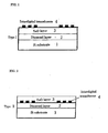
- FIGS 1 through 4 are sectional views of the surface acoustic wave devices of the present invention. These are referred to as Types I, II, III and IV for the sake of simplicity.
- Figure 1 is a view showing the Type I surface acoustic wave device.
- a diamond layer 2 is formed on a Si substrate 1
- a ZnO layer 3 is provided on the diamond layer 2
- interdigital transducers 4 are formed on the ZnO layer 3.
- This device corresponds to Types (1) to (4) described later.
- Figure 2 is a view showing the Type II surface acoustic wave device.
- a diamond layer 2 is formed on a Si substrate 1, and interdigital transducers 4 are formed on the diamond layer 2. Furthermore, a ZnO layer 3 is formed on the interdigital transducers 4. This device corresponds to Type (5) described later.
- Figure 3 is a view showing the Type III surface acoustic wave device.
- a diamond layer 2 is formed on a Si substrate 1
- interdigital transducers 4 are formed on the diamond layer 2
- a ZnO layer 3 is formed on the interdigital transducers 4.
- the structure obtained up to this stage is the same as that of the Type II surface acoustic wave device.
- a short-circuit electrode layer 5 is formed on the ZnO layer 3. This device corresponds to Types (6) and (7) described later.
- Figure 4 is a view showing the Type IV surface acoustic wave device.
- a diamond layer 2 is formed on a Si substrate 1
- a short-circuit electrode layer 5 is formed on the diamond layer 2
- a ZnO layer 3 is formed on the short-circuit electrode layer 5
- interdigital transducers 4 are formed on the ZnO layer 3.
- This device corresponds to Types (8) to (10) described later. Types (1) to (10) will be described later by referring to experimental results.
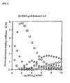
- the wavelength of the surface acoustic wave is ⁇ M .
- the abscissa represents 2 ⁇ H/ ⁇ M
- the ordinate represents phase velocity (m/s).
- the values indicated by squares represent a zeroth order mode
- the values indicated by lozenges represent a first order mode
- the values indicated by circles represent a second order mode
- the values indicated by triangles represent a third order mode
- the values indicated by x marks represent a fourth order mode
- the values indicated by + marks represent a fifth order mode.
- the phase velocity does not change depending on the difference in the structure (the difference in Types I, II, III and IV).
- Figure 6 is a graph showing the result of the measurement of the electromechanical coupling coefficient K 2 in the structure of Type I.
- the electromechanical coupling coefficient in the second order mode is large.
- the electromechanical coupling coefficient in the first order mode becomes large.
- the electromechanical coupling coefficients in the zeroth, second and fourth order modes become large.
- Figure 7 is a graph showing the result of the measurement of the electromechanical coupling coefficient K 2 in the structure of Type II.
- the electromechanical coupling coefficient in the first order mode is large.
- the electromechanical coupling coefficients in the zeroth and third order modes become large.
- the electromechanical coupling coefficients in the first, second and fifth order modes become large.
- Figure 8 is a graph showing the result of the measurement of the electromechanical coupling coefficient K 2 in the structure of Type III.
- the electromechanical coupling coefficients in the zeroth and first order modes are large.
- the electromechanical coupling coefficient in the third order mode becomes large.
- the electromechanical coupling coefficients in the first, second and fifth order modes become large.
- Figure 9 is a graph showing the result of the measurement of the electromechanical coupling coefficient K 2 in the structure of Type IV.
- the electromechanical coupling coefficients in the zeroth and first order modes are large.
- the electromechanical coupling coefficient in the first order mode becomes large.
- the electromechanical coupling coefficients in the zeroth, second, third and fourth order modes become large.
- Figure 10 is a graph showing the result of the measurement of a propagation loss in the structure of Type I.
- the propagation loss is plotted for the first order mode wherein the electromechanical coupling coefficient is large.
- the thicker the ZnO layer the smaller the propagation loss.
- Double electrodes were used as interdigital transducers to measure the propagation loss.
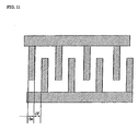
- the double interdigital transducers are structured as described in Figure 12 so that two electrode segments having a width of dm are arranged with a clearance of df therebetween whereby the two electrode segments are formed repeatedly at intervals of 2 ⁇ (df + dm).
- the electrodes can reduce the effect of scattering owing to the mismatch between the substance of the electrode section and the substance of the piezoelectric section.
- Type I Types 1, 2, 3 and 4
- the surface acoustic wave device of this type has a structure wherein a ZnO layer is stacked on a dielectric thin film comprising a diamond layer or a diamond layer formed on a substrate, and interdigital transducers for exciting a surface acoustic wave are disposed on the ZnO layer.
- the surface acoustic wave device of this type has a structure wherein a ZnO layer is stacked on a dielectric thin film comprising a diamond layer or a diamond layer formed on a substrate, and interdigital transducers for exciting a surface acoustic wave are disposed on the ZnO layer.
- the surface acoustic wave device of this type has a structure wherein a ZnO layer is stacked on a dielectric thin film comprising a diamond layer or a diamond layer formed on a substrate, and interdigital transducers for exciting a surface acoustic wave are disposed on the ZnO layer.
- the surface acoustic wave device of this type has a structure wherein a ZnO layer is stacked on a dielectric thin film comprising a diamond layer or a diamond layer formed on a substrate, and interdigital transducers for exciting a surface acoustic wave is disposed on the ZnO layer.
- Type II ... Type 5
- the surface acoustic wave device of this type has a structure wherein interdigital transducers for exciting a surface acoustic wave are disposed on a dielectric thin film comprising a diamond layer or a diamond layer formed on a substrate, and a ZnO layer is stacked on the interdigital transducers.
- Type III Types 6, 7
- the surface acoustic wave device of this type has a structure wherein interdigital transducers for exciting a surface acoustic wave are disposed on a dielectric thin film comprising a diamond layer or a diamond layer formed on a substrate, a ZnO layer is stacked on the interdigital transducers, and a short-circuit electrode is disposed on the ZnO layer.
- the surface acoustic wave device of this type has a structure wherein interdigital transducers for exciting a surface acoustic wave are disposed on a dielectric thin film comprising a diamond layer or a diamond layer formed on a substrate, a ZnO layer is stacked on the interdigital transducers, and a short-circuit electrode is disposed on the ZnO layer.
- the surface acoustic wave device of this type has a structure wherein a short-circuit electrode is stacked on a dielectric thin film comprising a diamond layer or a diamond layer formed on a substrate, a ZnO layer is stacked on the short-circuit electrode, and interdigital transducers for exciting a surface acoustic wave are disposed on the ZnO layer.
- the surface acoustic wave device of this type has a structure wherein a short-circuit electrode is stacked on a dielectric thin film comprising a diamond layer or a diamond layer formed on a substrate, a ZnO layer is stacked on the short-circuit electrode, and interdigital transducers for exciting a surface acoustic wave are disposed on the ZnO layer.
- the surface acoustic wave device of this type has a structure wherein a short-circuit electrode is stacked on a dielectric thin film comprising a diamond layer or a diamond layer formed on a substrate, a ZnO layer is stacked on the short-circuit electrode, and interdigital transducers for exciting a surface acoustic wave are disposed on the ZnO layer.
- the surface acoustic wave used for the devices of Type 1 to Type 10 may be a fundamental wave or a harmonic wave.
- both a natural diamond and a synthetic diamond can be used.
- a monocrystalline diamond, a polycrystalline diamond and an amorphous diamond can also be used.
- the diamond may be used as a single piece or a thin film formed on a substrate made of a different material.
- the diamond layer may be a part of the substrate or the whole of the substrate.
- the whole of the diamond layer may be insulating, and a part or the whole thereof may be semi-conducting.
- the substrate on which a diamond film is formed may be made of an inorganic material or a metal, such as Si, Mo or W, or glass, ceramics, oxide or nitride.
- the optimal value of (2 ⁇ H/ ⁇ M ) is the same for any substrate material.
- the value of 2 ⁇ H/ ⁇ M is 0.5 or more. It is further preferable that the value of 2 ⁇ H/ ⁇ M is 4.0 or more.
- the thin film of a diamond can be formed by known methods, such as the CVD method, plasma CVD method, PVD method and thermal filament method.
- various discharge methods such as the high-frequency/low-frequency glow discharge method and arc discharge method, can be used.
- a diamond film can be formed by using a compound including hydrogen atoms.
- a diamond film can be formed by using a gas capable of supplying halogen atoms and a compound including hydrogen atoms.
- the gas capable of supplying halogen atoms includes all of the compounds including halogen molecules as a matter of course, and compounds including halogen atoms in molecules thereof, such as halogenated organic compounds and halogenated inorganic compounds.
- These compounds are, for example, paraffin, olefin, alicyclic and aromatic organic compounds, such as methane fluoride, ethane fluoride, methane trifluoride and ethylene fluoride, and inorganic compounds, such as silane halide.
- the temperature of the substrate can be lowered by introducing a halogen gas into a film-forming chamber.
- a diamond film can be formed at 200°C to 900°C.
- the halogen gas have a large force of bonding with hydrogen and have a small atomic radius.
- fluoride compounds are preferably used.
- compounds including hydrogen atoms are aliphatic hydrocarbons, such as methane, ethane and propane, aromatic hydrocarbons, such as benzene and naphthalene, unsaturated hydrocarbons such as ethylene and propylene, and organic compounds having hetero atoms such as hydrazine.
- a high-purity diamond is an insulator having a low dielectric constant.
- a semi-conducting diamond can be formed by introducing impurities, such as B, Al, P and S, or by introducing lattice defects by ion implantation or electron beam irradiation.
- the single crystal of a semi-conducting diamond including B is rarely yielded as natural diamond and can be produced artificially by the ultra-high pressure method.
- the diamond layer or the diamond film formed on the substrate be an insulator and have a resistivity of 10 7 ⁇ cm or more, preferably 10 9 ⁇ cm or more.
- the surface of the diamond layer or the thin film of a diamond be flat to reduce scattering of the surface acoustic wave or other losses. The surface is required to be ground as necessary.
- the thin film of a single-crystal diamond formed by the epitaxial method can be used.
- the thin film of ZnO can be grown by the sputtering method or the CVD method so as to have high piezoelectric performance and so as to be excellent in the c-axis orientation property. It is preferable that the c-axis orientation of the thin film is 3° or less in terms of the ⁇ value and that the resistivity thereof is 10 5 ⁇ cm or more.
- the ZnO film have the c-axis orientation property.
- the c-axis orientation is defined herein that the (001) face of the ZnO film is parallel with the substrate.
- metals that have low resistivity values and can be formed into electrodes by etching for example, metals that can be subjected to vapor deposition at low temperatures, such as Au, Al and Cu, metals that can be formed into films at high temperatures, such as Ti, Mo and W, or a combination of two or more kinds of metals, such as Al vapor-deposited on Ti.
- metals that can be subjected to vapor deposition at low temperatures such as Au, Al and Cu
- metals that can be formed into films at high temperatures such as Ti, Mo and W, or a combination of two or more kinds of metals, such as Al vapor-deposited on Ti.
- Al or Ti The interdigital transducer can be formed as described below. After a metal film for the electrode is formed, a resist is applied uniformly to the surface of the metal film for the electrode.
- a mask formed of a transparent flat plate made from glass or the like having an interdigital transducer pattern is placed on the surface of a metal that has been applied with a resist, and the resist is exposed to light by light irradiation using a mercury lamp or the like. Or, without using a mask, the resist may be directly exposed to electron beams. After this, development is carried out to form a interdigital transducer in accordance with the resist pattern.
- the thicknesses of the interdigital transducers and the short-circuit electrode are not particularly restricted, the thicknesses preferably should be about 10 to 500 nm. When the thicknesses are less than 10 nm, the resistivity values become high and the losses increase. On the other hand, when the thicknesses are more than 500 nm, a mass addition effect causes a significant reflection of the surface acoustic wave.
- the wet etching method by using an alkaline solution, such as a sodium hydroxide solution, or by using an acidic solution, such as nitric acid, can be used for low-melting-point metals, such as Al.
- High-melting-point metals can also be etched by using a mixed solution of hydrofluoric acid and nitric acid.
- the electrodes can also be produced by the reactive ion etching method by using BCl 3 gas or the like.
- the chemical agents or gases used during electrode etching may degrade the surface of ZnO. To prevent this, it is possible to insert a thin insulator or a dielectric substance between the ZnO film and the interdigital transducers. In this case, the thickness of the thin film is required to be 50 nm or less to prevent the effect of the thin film.
- a diamond film having a thickness of 50 ⁇ m was formed on a Si substrate having dimensions of 10 mm x 10 mm x 0.3 mm by the microwave plasma CVD method, the surface of the diamond was polished to have various thicknesses of 1 to 30 ⁇ m by using a diamond coat grinder. A gas obtained by diluting CH 4 with H 2 100 times was used as the material of the diamond. Each of these films had a resistivity of 10 9 ⁇ cm or more.
- a piezoelectric body, interdigital transducers or a short-circuit electrode was formed on the polished surface of the diamond.
- a thin film of ZnO was formed as a piezoelectric body.
- the thin film of ZnO was obtained by sputtering polycrystalline ZnO by using the mixed gas of Ar and oxygen. The conditions of the sputtering are as follows: a substrate temperature of 400°C, an RF power of 160 W and a pressure of 2.7 Pa.
- the thickness of the ZnO film can be changed by changing the sputtering time.
- the ZnO films having thicknesses (2 ⁇ H/ ⁇ M ) in the range of 0.2 to 10 were formed.
- the interdigital transducers and the short-circuit electrode were vapor-deposited so as to have a thickness of 50 nm by the resistance heating method, and the electrodes were produced by the photolithography method.
- the wet etching method was used to produce the electrodes.
- the width of each electrode segment and the clearance between the electrode segments were 0.5 ⁇ m to 4 ⁇ m.
- a fundamental wave was formed in accordance with the electrode pattern shown in Figure 11 so as to have a wavelength ⁇ M of 2 to 16 ⁇ m.
- a harmonic wave was formed in accordance with the electrode pattern shown in Fig. 12 so as to be a third harmonic wave having a wavelength ⁇ M of 1.33 to 10.67 ⁇ m.
- Figure 5 is a graph showing a phase velocity depending on the thickness (2 ⁇ H/ ⁇ M ) of the ZnO film.
- Figure 6 is a graph showing a result of the measurement of the electromechanical coupling coefficient obtained by the structure shown in Fig. 1 depending on the thickness (2 ⁇ H/ ⁇ M ) of the ZnO film.
- Figure 7 is a graph showing a result of the measurement of the electromechanical coupling coefficient obtained by the structure shown in Fig. 2 depending on the thickness (2 ⁇ H/ ⁇ M ) of the ZnO film.
- Figure 8 is a graph showing a result of the measurement of the electromechanical coupling coefficient obtained by the structure shown in Fig. 3 depending on the thickness (2 ⁇ H/ ⁇ M ) of the ZnO film.
- Fig. 1 is a graph showing a phase velocity depending on the thickness (2 ⁇ H/ ⁇ M ) of the ZnO film.
- Figure 7 is a graph showing a result of the measurement of the electromechanical coupling coefficient obtained by the structure shown in Fig. 2 depending on the thickness (2
- FIG. 9 is a graph showing a result of the measurement of the electromechanical coupling coefficient obtained by the structure shown in Fig. 4 depending on the thickness (2 ⁇ H/ ⁇ M ) of the ZnO film.
- the structures selected depending on the thickness (2 ⁇ H/ ⁇ M ) and mode have high phase velocities of 5500 m/s or more and high electromechanical coupling coefficients of 0.5% or more, and can operate at higher frequencies in comparison with conventional materials, such as quarts crystal, LiNbO 3 , etc.
- Electrode patterns were formed in which the distances between the centers of the electrode segments of the input and output electrodes in the width direction were set, respectively, to values 40, 80, and 120 times the basic value.
- the propagation loss decreases, as the ZnO film is thicker.
- the setting of the film thickness for this time can reduce the propagation loss from 71 dB/cm to 66 dB/cm.
- the propagation loss clearly is reduced in comparison with the case of the conventional film thickness.
- a surface acoustic wave device having a small propagation loss, a large propagation velocity and a large electromechanical coupling coefficient. It is thus possible to easily provide a surface acoustic wave device operating in the high frequency range of several hundreds of MHz to several tens of GHz.
- the surface acoustic wave device can be used for band-pass filters, resonators, oscillators and convolvers.
Landscapes
- Physics & Mathematics (AREA)
- Acoustics & Sound (AREA)
- Surface Acoustic Wave Elements And Circuit Networks Thereof (AREA)
Abstract
Description
Claims (12)
- A surface acoustic wave device having a structure wherein a ZnO layer is stacked on a dielectric thin film comprising a diamond layer or a diamond layer formed on a substrate, and interdigital transducers for exciting a surface acoustic wave are disposed on said ZnO layer, being characterized by the use of a first order mode surface acoustic wave excited by a structure wherein the value of 2π·H/λM satisfies (2π·H/λM) = 3.0 to 3.2 where the thickness of said ZnO layer is H and the wavelength of the surface acoustic wave is λM.
- A surface acoustic wave device having a structure wherein a ZnO layer is stacked on a dielectric thin film comprising a diamond layer or a diamond layer formed on a substrate, and interdigital transducers for exciting a surface acoustic wave are disposed on said ZnO layer, being characterized by the use of a second order mode surface acoustic wave excited by a structure wherein the value of 2π·H/λM satisfies (2π·H/λM) = 4.2 to 6.0 where the thickness of said ZnO layer is H and the wavelength of the surface acoustic wave is λM.
- A surface acoustic wave device having a structure wherein a ZnO layer is stacked on a dielectric thin film comprising a diamond layer or a diamond layer formed on a substrate, and interdigital transducers for exciting a surface acoustic wave are disposed on said ZnO layer, being characterized by the use of a third order mode surface acoustic wave excited by a structure wherein the value of 2π·H/λM satisfies (2π·H/λM) = 6.0 to 8.5 where the thickness of said ZnO layer is H and the wavelength of the surface acoustic wave is λM.
- A surface acoustic wave device having a structure wherein a ZnO layer is stacked on a dielectric thin film comprising a diamond layer or a diamond layer formed on a substrate, and interdigital transducers for exciting a surface acoustic wave are disposed on said ZnO layer, being characterized by the use of a fourth order mode surface acoustic wave excited by a structure wherein the value of 2π·H/λM satisfies (2π·H/λM) = 9.0 to 10.0 where the thickness of said ZnO layer is H and the wavelength of the surface acoustic wave is λM.
- A surface acoustic wave device having a structure wherein interdigital transducers for exciting a surface acoustic wave are disposed on a dielectric thin film comprising a diamond layer or a diamond layer formed on a substrate, and a ZnO layer is stacked on said interdigital transducers, being characterized by the use of a fifth order mode surface acoustic wave excited by a structure wherein the value of 2π·H/λM satisfies (2π·H/λM) = 7.7 to 9.5 where the thickness of said ZnO layer is H and the wavelength of the surface acoustic wave is λM.
- A surface acoustic wave device having a structure wherein interdigital transducers for exciting a surface acoustic wave are disposed on a dielectric thin film comprising a diamond layer or a diamond layer formed on a substrate, a ZnO layer is stacked on said interdigital transducers, and a short-circuit electrode is disposed on said ZnO layer, being characterized by the use of the second order mode surface acoustic wave excited by a structure wherein the value of 2π·H/λM satisfies (2π·H/λM) = 7.2 to 8.5 where the thickness of said ZnO layer is H and the wavelength of the surface acoustic wave is λM.
- A surface acoustic wave device having a structure wherein interdigital transducers for exciting a surface acoustic wave are disposed on a dielectric thin film comprising a diamond layer or a diamond layer formed on a substrate, a ZnO layer is stacked on said interdigital transducers, and a short-circuit electrode is disposed on said ZnO layer, being characterized by the use of the fifth order mode surface acoustic wave excited by a structure wherein the value of 2π·H/λM satisfies (2π·H/λM) = 7.8 to 9.5 where the thickness of said ZnO layer is H and the wavelength of the surface acoustic wave is λM.
- A surface acoustic wave device having a structure wherein a short-circuit electrode is stacked on a dielectric thin film comprising a diamond layer or a diamond layer formed on a substrate, a ZnO layer is stacked on said short-circuit electrode, and interdigital transducers for exciting a surface acoustic wave are disposed on said ZnO layer, being characterized by the use of the second order mode surface acoustic wave excited by a structure wherein the value of 2π·H/λM satisfies (2π·H/λM) = 4.8 to 6.0 where the thickness of said ZnO layer is H and the wavelength of the surface acoustic wave is λM.
- A surface acoustic wave device having a structure wherein a short-circuit electrode is stacked on a dielectric thin film comprising a diamond layer or a diamond layer formed on a substrate, a ZnO layer is stacked on said short-circuit electrode, and interdigital transducers for exciting a surface acoustic wave are disposed on said ZnO layer, being characterized by the use of the third order mode surface acoustic wave excited by a structure wherein the value of 2π·H/λM satisfies (2π·H/λM) = 6.0 to 8.5 where the thickness of said ZnO layer is H and the wavelength of the surface acoustic wave is λ M.
- A surface acoustic wave device having a structure wherein a short-circuit electrode is stacked on a dielectric thin film comprising a diamond layer or a diamond layer formed on a substrate, a ZnO layer is stacked on said short-circuit electrode, and interdigital transducers for exciting a surface acoustic wave are disposed on said ZnO layer, being characterized by the use of the fourth order mode surface acoustic wave excited by a structure wherein the value of 2π·H/λM satisfies (2π·H/λM) = 9.0 to 10.0 where the thickness of said ZnO layer is H and the wavelength of the surface acoustic wave is λM.
- A surface acoustic wave device in accordance with any one of Claims 1 through 10, wherein the surface acoustic wave to be used is a fundamental wave.
- A surface acoustic wave device in accordance with any one of Claims 1 through 10, wherein the surface acoustic wave to be used is a harmonic wave.
Applications Claiming Priority (3)
| Application Number | Priority Date | Filing Date | Title |
|---|---|---|---|
| JP29363199 | 1999-10-15 | ||
| JP29363199 | 1999-10-15 | ||
| PCT/JP2000/006944 WO2001028089A1 (en) | 1999-10-15 | 2000-10-04 | Saw device |
Publications (3)
| Publication Number | Publication Date |
|---|---|
| EP1225693A1 true EP1225693A1 (en) | 2002-07-24 |
| EP1225693A4 EP1225693A4 (en) | 2005-08-17 |
| EP1225693B1 EP1225693B1 (en) | 2008-05-21 |
Family
ID=17797219
Family Applications (1)
| Application Number | Title | Priority Date | Filing Date |
|---|---|---|---|
| EP00964683A Expired - Lifetime EP1225693B1 (en) | 1999-10-15 | 2000-10-04 | Saw device |
Country Status (4)
| Country | Link |
|---|---|
| US (1) | US6984918B1 (en) |
| EP (1) | EP1225693B1 (en) |
| DE (1) | DE60038970D1 (en) |
| WO (1) | WO2001028089A1 (en) |
Cited By (1)
| Publication number | Priority date | Publication date | Assignee | Title |
|---|---|---|---|---|
| WO2018095311A1 (en) | 2016-11-24 | 2018-05-31 | Huawei Technologies Co., Ltd. | Surface acoustic wave device |
Families Citing this family (4)
| Publication number | Priority date | Publication date | Assignee | Title |
|---|---|---|---|---|
| US7642693B2 (en) * | 2003-05-15 | 2010-01-05 | National Institute Of Advanced Industrial Science And Technology | Wurtzite thin film, laminate containing wurtzite crystalline layer and their manufacturing methods |
| WO2009023100A2 (en) * | 2007-08-14 | 2009-02-19 | Skyworks Solutions, Inc. | Method for forming a multi-layer electrode underlying a piezoelectric layer and related structure |
| US9608589B2 (en) | 2010-10-26 | 2017-03-28 | Avago Technologies General Ip (Singapore) Pte. Ltd. | Method of forming acoustic resonator using intervening seed layer |
| CN113114158A (en) * | 2021-05-11 | 2021-07-13 | 中国科学院上海微系统与信息技术研究所 | Lamb wave resonator and elastic wave device |
Family Cites Families (11)
| Publication number | Priority date | Publication date | Assignee | Title |
|---|---|---|---|---|
| JPS6462911A (en) | 1987-09-03 | 1989-03-09 | Sumitomo Electric Industries | Surface acoustic wave element |
| JP2885349B2 (en) | 1989-12-26 | 1999-04-19 | 住友電気工業株式会社 | Surface acoustic wave device |
| JP3132078B2 (en) | 1991-09-19 | 2001-02-05 | 住友電気工業株式会社 | Surface acoustic wave device and method of manufacturing the same |
| JP3205976B2 (en) * | 1992-09-14 | 2001-09-04 | 住友電気工業株式会社 | Surface acoustic wave device |
| EP0635938B1 (en) * | 1993-07-20 | 1998-04-15 | AVL List GmbH | Piezoelectric crystal element |
| DE69424737T2 (en) * | 1993-10-08 | 2000-09-28 | Matsushita Electric Ind Co Ltd | Acoustic surface wave filter |
| JP3204290B2 (en) * | 1995-02-09 | 2001-09-04 | 住友電気工業株式会社 | Surface acoustic wave device |
| JP3205978B2 (en) | 1995-08-08 | 2001-09-04 | 住友電気工業株式会社 | Surface acoustic wave device |
| US6072263A (en) * | 1996-08-09 | 2000-06-06 | Toda; Kohji | Surface acoustic wave transducing device |
| DE69723957T2 (en) * | 1996-10-18 | 2004-06-17 | Tdk Corp. | ACOUSTIC SURFACE WAVE ARRANGEMENT |
| JP3275297B2 (en) | 1996-11-07 | 2002-04-15 | 住友電気工業株式会社 | Surface acoustic wave device and manufacturing method |
-
2000
- 2000-10-04 EP EP00964683A patent/EP1225693B1/en not_active Expired - Lifetime
- 2000-10-04 WO PCT/JP2000/006944 patent/WO2001028089A1/en not_active Ceased
- 2000-10-04 DE DE60038970T patent/DE60038970D1/en not_active Expired - Lifetime
- 2000-10-04 US US10/089,804 patent/US6984918B1/en not_active Expired - Fee Related
Cited By (4)
| Publication number | Priority date | Publication date | Assignee | Title |
|---|---|---|---|---|
| WO2018095311A1 (en) | 2016-11-24 | 2018-05-31 | Huawei Technologies Co., Ltd. | Surface acoustic wave device |
| CN109997307A (en) * | 2016-11-24 | 2019-07-09 | 华为技术有限公司 | Surface acoustic wave device |
| EP3542462A4 (en) * | 2016-11-24 | 2019-12-11 | Huawei Technologies Co., Ltd. | ACOUSTIC SURFACE WAVE DEVICE |
| US10658564B2 (en) | 2016-11-24 | 2020-05-19 | Huawei Technologies Co., Ltd. | Surface acoustic wave device |
Also Published As
| Publication number | Publication date |
|---|---|
| US6984918B1 (en) | 2006-01-10 |
| WO2001028089A1 (en) | 2001-04-19 |
| DE60038970D1 (en) | 2008-07-03 |
| EP1225693A4 (en) | 2005-08-17 |
| EP1225693B1 (en) | 2008-05-21 |
Similar Documents
| Publication | Publication Date | Title |
|---|---|---|
| EP0435189B1 (en) | Surface acoustic wave device | |
| EP0588261B1 (en) | Surface acoustic wave element | |
| US7579759B2 (en) | Surface acoustic wave (SAW) devices based on cubic boron nitride/diamond composite structures | |
| EP0556811B1 (en) | Surface acoustic wave device | |
| US5838090A (en) | Surface acoustic wave device | |
| JP3282645B2 (en) | Surface acoustic wave device | |
| EP0691739B1 (en) | Surface acoustic wave device | |
| US6642813B1 (en) | Surface acoustic wave device utilizing a ZnO layer and a diamond layer | |
| EP0766383A2 (en) | Diamond-ZnO surface acoustic wave device having relatively thinner ZnO piezoelectric layer | |
| US6984918B1 (en) | Saw device | |
| JPWO2001028090A1 (en) | Surface Acoustic Wave Device | |
| JP3132078B2 (en) | Surface acoustic wave device and method of manufacturing the same | |
| US6469416B1 (en) | Surface acoustic wave device | |
| JP3341759B2 (en) | Surface acoustic wave device | |
| US6713941B2 (en) | Surface acoustic wave element | |
| JP3132065B2 (en) | Surface acoustic wave device and method of manufacturing the same | |
| JP3132074B2 (en) | Diamond surface acoustic wave device |
Legal Events
| Date | Code | Title | Description |
|---|---|---|---|
| PUAI | Public reference made under article 153(3) epc to a published international application that has entered the european phase |
Free format text: ORIGINAL CODE: 0009012 |
|
| 17P | Request for examination filed |
Effective date: 20020211 |
|
| AK | Designated contracting states |
Kind code of ref document: A1 Designated state(s): AT BE CH CY DE DK ES FI FR GB GR IE IT LI LU MC NL PT SE |
|
| AX | Request for extension of the european patent |
Free format text: AL;LT;LV;MK;RO;SI |
|
| RBV | Designated contracting states (corrected) |
Designated state(s): DE DK FR GB |
|
| RAP1 | Party data changed (applicant data changed or rights of an application transferred) |
Owner name: SEIKO EPSON CORPORATION |
|
| A4 | Supplementary search report drawn up and despatched |
Effective date: 20050706 |
|
| RIC1 | Information provided on ipc code assigned before grant |
Ipc: 7H 03H 9/145 A Ipc: 7H 03H 9/02 B |
|
| GRAP | Despatch of communication of intention to grant a patent |
Free format text: ORIGINAL CODE: EPIDOSNIGR1 |
|
| GRAS | Grant fee paid |
Free format text: ORIGINAL CODE: EPIDOSNIGR3 |
|
| GRAA | (expected) grant |
Free format text: ORIGINAL CODE: 0009210 |
|
| AK | Designated contracting states |
Kind code of ref document: B1 Designated state(s): DE DK FR GB |
|
| REG | Reference to a national code |
Ref country code: GB Ref legal event code: FG4D |
|
| REF | Corresponds to: |
Ref document number: 60038970 Country of ref document: DE Date of ref document: 20080703 Kind code of ref document: P |
|
| PG25 | Lapsed in a contracting state [announced via postgrant information from national office to epo] |
Ref country code: DK Free format text: LAPSE BECAUSE OF FAILURE TO SUBMIT A TRANSLATION OF THE DESCRIPTION OR TO PAY THE FEE WITHIN THE PRESCRIBED TIME-LIMIT Effective date: 20080521 |
|
| PLBE | No opposition filed within time limit |
Free format text: ORIGINAL CODE: 0009261 |
|
| STAA | Information on the status of an ep patent application or granted ep patent |
Free format text: STATUS: NO OPPOSITION FILED WITHIN TIME LIMIT |
|
| 26N | No opposition filed |
Effective date: 20090224 |
|
| REG | Reference to a national code |
Ref country code: FR Ref legal event code: PLFP Year of fee payment: 16 |
|
| PGFP | Annual fee paid to national office [announced via postgrant information from national office to epo] |
Ref country code: GB Payment date: 20150930 Year of fee payment: 16 |
|
| PGFP | Annual fee paid to national office [announced via postgrant information from national office to epo] |
Ref country code: FR Payment date: 20150908 Year of fee payment: 16 |
|
| PGFP | Annual fee paid to national office [announced via postgrant information from national office to epo] |
Ref country code: DE Payment date: 20150929 Year of fee payment: 16 |
|
| REG | Reference to a national code |
Ref country code: DE Ref legal event code: R119 Ref document number: 60038970 Country of ref document: DE |
|
| GBPC | Gb: european patent ceased through non-payment of renewal fee |
Effective date: 20161004 |
|
| REG | Reference to a national code |
Ref country code: FR Ref legal event code: ST Effective date: 20170630 |
|
| PG25 | Lapsed in a contracting state [announced via postgrant information from national office to epo] |
Ref country code: GB Free format text: LAPSE BECAUSE OF NON-PAYMENT OF DUE FEES Effective date: 20161004 Ref country code: DE Free format text: LAPSE BECAUSE OF NON-PAYMENT OF DUE FEES Effective date: 20170503 Ref country code: FR Free format text: LAPSE BECAUSE OF NON-PAYMENT OF DUE FEES Effective date: 20161102 |