EP1223584A2 - Memory device and method for handling out of range addresses - Google Patents
Memory device and method for handling out of range addresses Download PDFInfo
- Publication number
- EP1223584A2 EP1223584A2 EP01205211A EP01205211A EP1223584A2 EP 1223584 A2 EP1223584 A2 EP 1223584A2 EP 01205211 A EP01205211 A EP 01205211A EP 01205211 A EP01205211 A EP 01205211A EP 1223584 A2 EP1223584 A2 EP 1223584A2
- Authority
- EP
- European Patent Office
- Prior art keywords
- storage units
- memory device
- rows
- address information
- range
- Prior art date
- Legal status (The legal status is an assumption and is not a legal conclusion. Google has not performed a legal analysis and makes no representation as to the accuracy of the status listed.)
- Granted
Links
Images


Classifications
-
- G—PHYSICS
- G11—INFORMATION STORAGE
- G11C—STATIC STORES
- G11C8/00—Arrangements for selecting an address in a digital store
Definitions
- the present invention relates in general to memory access technology and more particularly to a memory device and method for handling out of range addresses.
- a conventional memory device includes an array of memory cells accessed by a row select signal. As long as a valid address is applied, a single row is selected and each bitline for the selected row is driven to a known state by the selected memory cells. However, if an out of range address is applied, none of the rows within the memory device are selected, causing the bitlines to be undriven and float to an unknown logic state. If provisions are not made within the memory device to handle an out of range address, problems such as high current and/or metastability will occur.
- Another technique for solving the floating bitline problem for out of range addresses includes using a voltage or current differential sensing scheme.
- this scheme has no provision to guarantee the data read from invalid address locations. It is assumed that slight imbalances in the feedback of the sense amplifier used in such a scheme will eventually cause the bitline to resolve to either one logic level or the other after some period of time. While it is true that the sense amplifier will eventually resolve to a full logic state, excess power is consumed every time an out of range address condition occurs. The excess power consumption results from the metastable condition created when the sense amplifier is enabled with no differential voltage present on the bitlines.
- a memory device and method are provided that substantially eliminate or greatly reduce disadvantages and problems of conventional memory devices.
- a memory device for handling out of range addresses that includes a memory array having a plurality of storage units arranged in a plurality of rows and a bitline driver also having a plurality of storage units.
- a row decoder receives address information and determines which one of the plurality of rows of the memory array is to be accessed.
- a row selector selects one of the plurality of rows determined by the row decoder in order to output values stored in its associated storage units.
- An out of range decoder receives address information and determines that none of the plurality of rows of the memory array is to be accessed for the received address information.
- An out of range selector selects the storage units of the bitline driver in response to the out of range decoder determining that the received address information does not access any of the plurality of rows of the memory array in order to provide an output from the memory device.
- the present invention provides various technical advantages over conventional memory devices. For example, one technical advantage is to eliminate the use of feedback latches and sense amplifiers to drive the bitlines of a memory during the occurrence of an out of range address. Another technical advantage is to detect for an out of range address. Yet another technical advantage is to drive the bitlines of the memory device upon the occurrence of an out of range address. Further technical advantages include predictable data output when accessing out of range addresses, faster access times, lower voltage functionality, and no floating bitlines. Other technical advantages may be readily apparent to those skilled in the art from the following figures, description, and claims.
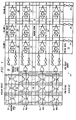
- FIGURE 1 is a block diagram of a memory device 10.
- Memory device 10 includes a memory array 12 having a plurality of storage units 14 arranged in a plurality of rows 16.
- Memory device 10 includes a row decoder 18, a row selector 20, and a bitline sensor 22.
- Memory device 10 also includes an out of range decoder 24, an out of range selector 26, and a bitline driver 28.
- Bitline driver 28 includes a plurality of storage units 30 arranged in a single row 32.
- row decoder 18 receives address information and determines the appropriate row 16 corresponding to the received address information.
- the identified row 16 determined by row decoder 18 drives row selector 20 to enable storage units 14 associated with the identified row 16 to provide their outputs onto respective bitlines 34 for determination by bitline sensor 22.
- out of range decoder 24 recognizes an occurrence of an out of range address and appropriately causes out of range selector 26 to drive bitline driver 28 in order to provide an output onto bitlines 34 from storage units 30 of single row 32.
- Storage units 30 may have pre-programmed values stored therein to indicate that an out of range address was received by memory device 10.
- Storage units 30, as well as storage units 14 in memory array 12, may include p-channel elements, n-channel elements, and/or a memory cell circuit as shown.
- Out of Range decoder 24 may identify an out of range address using boolean decoding techniques.
- FIGURE 2 shows an alternative memory device 40.
- Memory device 40 uses a feedback latch 42 on each bitline 34 instead of a separate bitline driver 28 with storage units 30 found in memory device 10.
- Out of range decoder 24 identifies the occurrence of an out of range address and causes out of range selector 26 to enable feedback latches 42 on each bitline 34 of row 32.
- Feedback latches 42 hold the bitlines 34 at their previous state in order to provide outputs during an out of range address occurrence.
- feedback latches 42 Upon determination of a valid in range address, feedback latches 42 are disabled and the appropriate outputs from storage units 14 of the determined row 16 identified by row decoder 18 and row selector 20 may be placed onto respective bitlines 34.
- FIGURE 3 shows another alternative memory device 50.
- Memory device 50 is used in clocking implementations.
- Memory device 50 receives a precharge control signal on a precharge line 52 to precharge each row line 16 and the out of range row line 32. If row decoder 18 receives address information that indicates one of the plurality of rows 16 is to be accessed, row selector 20 allows the identified row 16 to pull down the precharge line to a logic low state so that values from storage units 14 of the identified row 16 are placed onto bitlines 34 upon receiving an enable control signal 54.. This pulling down of the precharge line by the identified row 16 also disables out of range row 32 through appropriate logic in out of range selector 26.
- precharge line 52 When there is no row 16 identified by row decoder 18, then the address information indicates an out of range address. In this case, there is no pull down of precharge line 52 by any decoded row 16. By not being pulled down to a logic low state, precharge line 52 now activates out of range selector 26 to drive storage units 30 and provide output values therefrom onto bitlines 34 in response to enable control signal 54. In this manner, out of range addresses can be properly handled by memory device 50.
Landscapes
- Engineering & Computer Science (AREA)
- Microelectronics & Electronic Packaging (AREA)
- Static Random-Access Memory (AREA)
- Techniques For Improving Reliability Of Storages (AREA)
- Storage Device Security (AREA)
- Indexing, Searching, Synchronizing, And The Amount Of Synchronization Travel Of Record Carriers (AREA)
- Credit Cards Or The Like (AREA)
- Cookers (AREA)
- Dram (AREA)
Abstract
Description
Claims (15)
- A memory device for handling out of range addresses, comprising:a memory array having a plurality of storage units arranged in a plurality of rows;a bitline driver having a plurality of storage units;a row decoder operable to receive address information, the row decoder operable to determine which one of the plurality of rows of the memory array is to be accessed;a row selector operable to select one of the plurality of rows determined by the row decoder in order to output values stored in its associated storage units onto respective bitlines;an out of range decoder operable to receive address information, the out of range decoder operable to determine that none of the plurality of rows of the memory array is to be accessed for the received address information;an out of range selector operable to select the storage units of the bitline driver in response to the out of range decoder determining that the received address information does not access any of the plurality of rows of the memory array.
- The memory device of Claim 1, wherein the plurality of storage units of the bitline driver include pre-determined values programmed therein.
- The memory device of Claim 1, wherein each of the plurality of storage units of the bitline driver include a p-channel element.
- The memory device of Claim 1, wherein each of the plurality of storage units of the bitline driver include an n-channel element.
- The memory device of Claim 1, wherein each of the plurality of storage units of the bitline driver includes a memory cell circuit.
- The memory device of Claim 1, wherein each of the plurality of storage units of the bitline driver includes a feedback latch.
- The memory device of Claim 6, wherein the feedback latch of each of the plurality of storage units of the bitline driver are enabled upon determining that the address information does not access any of the plurality of rows of the memory array.
- The memory device of Claim 6, wherein the feedback latch of each of the plurality of storage units of the bitline driver maintains a previous value placed on the bitlines in response to the address information not accessing any of the plurality of rows of the memory array.
- The memory device of Claim 6, wherein the feedback latch of each of the plurality of storage units of the bitline driver is disabled upon determining that the address information accesses one of the plurality of rows of the memory array.
- The memory device of Claim 1, wherein the out of range selector includes a precharge control signal and an enable control signal.
- A memory device for handling out of range addresses, comprising:a memory array having a plurality of storage units arranged in a plurality of rows, each storage unit of the memory array operable to provide an output onto an associated bitline, each storage unit being a memory cell circuit;a bitline driver having a plurality of storage units, each storage unit of the bitline drive operable to provide an output onto the associated bitlines;a row decoder operable to receive address information, the row decoder operable to determine which one of the plurality of rows of the memory array is to be accessed;a row selector operable to select one of the plurality of rows determined by the row decoder in order to output values stored in its associated storage units onto the associated bitlines;a boolean decoder operable to receive address information, the boolean decoder operable to determine that none of the plurality of rows of the memory array is to be accessed for the received address information;a boolean selector operable to select the storage units of the bitline driver in response to the boolean decoder determining that the received address information does not access any of the plurality of rows of the memory array.
- The memory device of Claim 11, wherein each storage unit of the bitline driver is preprogrammed with a value to output on the associated bitlines.
- The memory device of Claim 11, wherein each storage unit of the bitline driver includes a feedback latch enabled by the boolean selector.
- The memory device of Claim 13, wherein the feedback latch of each storage unit of the bitline driver is operable to maintain a previous output value on the associated bitlines upon being enabled.
- The memory device of Claim 11, wherein the storage units of the bitline driver include p-channel and/or n-channel elements.
Applications Claiming Priority (2)
| Application Number | Priority Date | Filing Date | Title |
|---|---|---|---|
| US25877300P | 2000-12-29 | 2000-12-29 | |
| US258773 | 2000-12-29 |
Publications (3)
| Publication Number | Publication Date |
|---|---|
| EP1223584A2 true EP1223584A2 (en) | 2002-07-17 |
| EP1223584A3 EP1223584A3 (en) | 2003-05-07 |
| EP1223584B1 EP1223584B1 (en) | 2008-11-05 |
Family
ID=22982059
Family Applications (1)
| Application Number | Title | Priority Date | Filing Date |
|---|---|---|---|
| EP01205211A Expired - Lifetime EP1223584B1 (en) | 2000-12-29 | 2001-12-28 | Memory device and method for handling out of range addresses |
Country Status (4)
| Country | Link |
|---|---|
| EP (1) | EP1223584B1 (en) |
| JP (1) | JP4152629B2 (en) |
| AT (1) | ATE413682T1 (en) |
| DE (1) | DE60136438D1 (en) |
Family Cites Families (1)
| Publication number | Priority date | Publication date | Assignee | Title |
|---|---|---|---|---|
| US5287321A (en) * | 1992-01-24 | 1994-02-15 | Vlsi Technology, Inc. | Illegal address detector for semiconductor memories |
-
2001
- 2001-12-27 JP JP2001397655A patent/JP4152629B2/en not_active Expired - Fee Related
- 2001-12-28 DE DE60136438T patent/DE60136438D1/en not_active Expired - Lifetime
- 2001-12-28 EP EP01205211A patent/EP1223584B1/en not_active Expired - Lifetime
- 2001-12-28 AT AT01205211T patent/ATE413682T1/en not_active IP Right Cessation
Also Published As
| Publication number | Publication date |
|---|---|
| JP2002208283A (en) | 2002-07-26 |
| JP4152629B2 (en) | 2008-09-17 |
| EP1223584A3 (en) | 2003-05-07 |
| ATE413682T1 (en) | 2008-11-15 |
| EP1223584B1 (en) | 2008-11-05 |
| DE60136438D1 (en) | 2008-12-18 |
Similar Documents
| Publication | Publication Date | Title |
|---|---|---|
| US11790971B2 (en) | Ferroelectric random access memory device and method for operating read and write thereof | |
| JP3703951B2 (en) | Nonvolatile semiconductor memory device | |
| US6891745B2 (en) | Design concept for SRAM read margin | |
| US5848015A (en) | Bitline precharge halt access mode for low power operation of a memory device | |
| US7231488B2 (en) | Self-refresh system and method for dynamic random access memory | |
| JP2004134026A (en) | Semiconductor memory device and its control method | |
| JPH01178193A (en) | Semiconductor storage device | |
| KR20060002967A (en) | Memory Device with Sense Amplifier and Self-Timed Latch | |
| EP3355308B1 (en) | Memory devices and operation methods thereof | |
| WO1998006100A9 (en) | Bitline precharge halt access mode for low power operation of a memory device | |
| CN106710625B (en) | Burst mode read controllable SRAM | |
| KR100805528B1 (en) | Selective Refresh Method and System in Semiconductor Memory Device | |
| US7064984B2 (en) | Circuit and method for reducing leakage current in a row driver circuit in a flash memory during a standby mode of operation | |
| KR0136448B1 (en) | Semiconductor memory device with error self-correction function | |
| US6414900B1 (en) | Memory device and method for handling out of range addresses | |
| US5784320A (en) | Method and apparatus for reducing power consumption in a memory by employing a conditional write controller | |
| US6707707B2 (en) | SRAM power-up system and method | |
| JP2001084760A (en) | Semiconductor storage device | |
| KR910014938A (en) | Integrated Circuit Memory with Enhanced DI / DT Control | |
| US7440352B2 (en) | Semiconductor memory device capable of selectively refreshing word lines | |
| US7675806B2 (en) | Low voltage memory device and method thereof | |
| US7158400B2 (en) | Method of operating dynamic random access memory | |
| EP1761932B1 (en) | Dram with half and full density operation | |
| US20250124998A1 (en) | Semiconductor device for controlling operating power supplied to word line driver | |
| KR20050016699A (en) | Worldline latching in semiconductor memories |
Legal Events
| Date | Code | Title | Description |
|---|---|---|---|
| PUAI | Public reference made under article 153(3) epc to a published international application that has entered the european phase |
Free format text: ORIGINAL CODE: 0009012 |
|
| AK | Designated contracting states |
Kind code of ref document: A2 Designated state(s): AT BE CH CY DE DK ES FI FR GB GR IE IT LI LU MC NL PT SE TR |
|
| AX | Request for extension of the european patent |
Free format text: AL;LT;LV;MK;RO;SI |
|
| PUAL | Search report despatched |
Free format text: ORIGINAL CODE: 0009013 |
|
| AK | Designated contracting states |
Designated state(s): AT BE CH CY DE DK ES FI FR GB GR IE IT LI LU MC NL PT SE TR |
|
| AX | Request for extension of the european patent |
Extension state: AL LT LV MK RO SI |
|
| 17P | Request for examination filed |
Effective date: 20031107 |
|
| AKX | Designation fees paid |
Designated state(s): AT BE CH CY DE DK ES FI FR GB GR IE IT LI LU MC NL PT SE TR |
|
| 17Q | First examination report despatched |
Effective date: 20070111 |
|
| GRAP | Despatch of communication of intention to grant a patent |
Free format text: ORIGINAL CODE: EPIDOSNIGR1 |
|
| GRAS | Grant fee paid |
Free format text: ORIGINAL CODE: EPIDOSNIGR3 |
|
| GRAA | (expected) grant |
Free format text: ORIGINAL CODE: 0009210 |
|
| AK | Designated contracting states |
Kind code of ref document: B1 Designated state(s): AT BE CH CY DE DK ES FI FR GB GR IE IT LI LU MC NL PT SE TR |
|
| REG | Reference to a national code |
Ref country code: GB Ref legal event code: FG4D |
|
| REG | Reference to a national code |
Ref country code: CH Ref legal event code: EP |
|
| REG | Reference to a national code |
Ref country code: IE Ref legal event code: FG4D |
|
| REF | Corresponds to: |
Ref document number: 60136438 Country of ref document: DE Date of ref document: 20081218 Kind code of ref document: P |
|
| PG25 | Lapsed in a contracting state [announced via postgrant information from national office to epo] |
Ref country code: ES Free format text: LAPSE BECAUSE OF FAILURE TO SUBMIT A TRANSLATION OF THE DESCRIPTION OR TO PAY THE FEE WITHIN THE PRESCRIBED TIME-LIMIT Effective date: 20090216 Ref country code: AT Free format text: LAPSE BECAUSE OF FAILURE TO SUBMIT A TRANSLATION OF THE DESCRIPTION OR TO PAY THE FEE WITHIN THE PRESCRIBED TIME-LIMIT Effective date: 20081105 |
|
| PG25 | Lapsed in a contracting state [announced via postgrant information from national office to epo] |
Ref country code: FI Free format text: LAPSE BECAUSE OF FAILURE TO SUBMIT A TRANSLATION OF THE DESCRIPTION OR TO PAY THE FEE WITHIN THE PRESCRIBED TIME-LIMIT Effective date: 20081105 |
|
| PG25 | Lapsed in a contracting state [announced via postgrant information from national office to epo] |
Ref country code: DK Free format text: LAPSE BECAUSE OF FAILURE TO SUBMIT A TRANSLATION OF THE DESCRIPTION OR TO PAY THE FEE WITHIN THE PRESCRIBED TIME-LIMIT Effective date: 20081105 Ref country code: MC Free format text: LAPSE BECAUSE OF NON-PAYMENT OF DUE FEES Effective date: 20081231 Ref country code: BE Free format text: LAPSE BECAUSE OF FAILURE TO SUBMIT A TRANSLATION OF THE DESCRIPTION OR TO PAY THE FEE WITHIN THE PRESCRIBED TIME-LIMIT Effective date: 20081105 |
|
| REG | Reference to a national code |
Ref country code: CH Ref legal event code: PL |
|
| PG25 | Lapsed in a contracting state [announced via postgrant information from national office to epo] |
Ref country code: SE Free format text: LAPSE BECAUSE OF FAILURE TO SUBMIT A TRANSLATION OF THE DESCRIPTION OR TO PAY THE FEE WITHIN THE PRESCRIBED TIME-LIMIT Effective date: 20090205 Ref country code: PT Free format text: LAPSE BECAUSE OF FAILURE TO SUBMIT A TRANSLATION OF THE DESCRIPTION OR TO PAY THE FEE WITHIN THE PRESCRIBED TIME-LIMIT Effective date: 20090406 |
|
| PLBE | No opposition filed within time limit |
Free format text: ORIGINAL CODE: 0009261 |
|
| STAA | Information on the status of an ep patent application or granted ep patent |
Free format text: STATUS: NO OPPOSITION FILED WITHIN TIME LIMIT |
|
| 26N | No opposition filed |
Effective date: 20090806 |
|
| PG25 | Lapsed in a contracting state [announced via postgrant information from national office to epo] |
Ref country code: CH Free format text: LAPSE BECAUSE OF NON-PAYMENT OF DUE FEES Effective date: 20081231 Ref country code: LI Free format text: LAPSE BECAUSE OF NON-PAYMENT OF DUE FEES Effective date: 20081231 |
|
| PG25 | Lapsed in a contracting state [announced via postgrant information from national office to epo] |
Ref country code: IE Free format text: LAPSE BECAUSE OF NON-PAYMENT OF DUE FEES Effective date: 20081228 |
|
| PG25 | Lapsed in a contracting state [announced via postgrant information from national office to epo] |
Ref country code: LU Free format text: LAPSE BECAUSE OF NON-PAYMENT OF DUE FEES Effective date: 20081228 Ref country code: CY Free format text: LAPSE BECAUSE OF FAILURE TO SUBMIT A TRANSLATION OF THE DESCRIPTION OR TO PAY THE FEE WITHIN THE PRESCRIBED TIME-LIMIT Effective date: 20081105 |
|
| PG25 | Lapsed in a contracting state [announced via postgrant information from national office to epo] |
Ref country code: TR Free format text: LAPSE BECAUSE OF FAILURE TO SUBMIT A TRANSLATION OF THE DESCRIPTION OR TO PAY THE FEE WITHIN THE PRESCRIBED TIME-LIMIT Effective date: 20081105 |
|
| PG25 | Lapsed in a contracting state [announced via postgrant information from national office to epo] |
Ref country code: GR Free format text: LAPSE BECAUSE OF FAILURE TO SUBMIT A TRANSLATION OF THE DESCRIPTION OR TO PAY THE FEE WITHIN THE PRESCRIBED TIME-LIMIT Effective date: 20090206 |
|
| PG25 | Lapsed in a contracting state [announced via postgrant information from national office to epo] |
Ref country code: IT Free format text: LAPSE BECAUSE OF FAILURE TO SUBMIT A TRANSLATION OF THE DESCRIPTION OR TO PAY THE FEE WITHIN THE PRESCRIBED TIME-LIMIT Effective date: 20081105 |
|
| REG | Reference to a national code |
Ref country code: FR Ref legal event code: PLFP Year of fee payment: 15 |
|
| REG | Reference to a national code |
Ref country code: FR Ref legal event code: PLFP Year of fee payment: 16 |
|
| PGFP | Annual fee paid to national office [announced via postgrant information from national office to epo] |
Ref country code: GB Payment date: 20161125 Year of fee payment: 16 Ref country code: NL Payment date: 20161207 Year of fee payment: 16 Ref country code: FR Payment date: 20161117 Year of fee payment: 16 |
|
| PGFP | Annual fee paid to national office [announced via postgrant information from national office to epo] |
Ref country code: DE Payment date: 20161220 Year of fee payment: 16 |
|
| REG | Reference to a national code |
Ref country code: DE Ref legal event code: R119 Ref document number: 60136438 Country of ref document: DE |
|
| REG | Reference to a national code |
Ref country code: NL Ref legal event code: MM Effective date: 20180101 |
|
| GBPC | Gb: european patent ceased through non-payment of renewal fee |
Effective date: 20171228 |
|
| PG25 | Lapsed in a contracting state [announced via postgrant information from national office to epo] |
Ref country code: NL Free format text: LAPSE BECAUSE OF NON-PAYMENT OF DUE FEES Effective date: 20180101 |
|
| REG | Reference to a national code |
Ref country code: FR Ref legal event code: ST Effective date: 20180831 |
|
| PG25 | Lapsed in a contracting state [announced via postgrant information from national office to epo] |
Ref country code: DE Free format text: LAPSE BECAUSE OF NON-PAYMENT OF DUE FEES Effective date: 20180703 Ref country code: FR Free format text: LAPSE BECAUSE OF NON-PAYMENT OF DUE FEES Effective date: 20180102 |
|
| PG25 | Lapsed in a contracting state [announced via postgrant information from national office to epo] |
Ref country code: GB Free format text: LAPSE BECAUSE OF NON-PAYMENT OF DUE FEES Effective date: 20171228 |