EP1223458A2 - Tiled display - Google Patents
Tiled display Download PDFInfo
- Publication number
- EP1223458A2 EP1223458A2 EP02075008A EP02075008A EP1223458A2 EP 1223458 A2 EP1223458 A2 EP 1223458A2 EP 02075008 A EP02075008 A EP 02075008A EP 02075008 A EP02075008 A EP 02075008A EP 1223458 A2 EP1223458 A2 EP 1223458A2
- Authority
- EP
- European Patent Office
- Prior art keywords
- tiles
- pixels
- aligned
- display
- tile
- Prior art date
- Legal status (The legal status is an assumption and is not a legal conclusion. Google has not performed a legal analysis and makes no representation as to the accuracy of the status listed.)
- Withdrawn
Links
Images


Classifications
-
- H—ELECTRICITY
- H10—SEMICONDUCTOR DEVICES; ELECTRIC SOLID-STATE DEVICES NOT OTHERWISE PROVIDED FOR
- H10K—ORGANIC ELECTRIC SOLID-STATE DEVICES
- H10K59/00—Integrated devices, or assemblies of multiple devices, comprising at least one organic light-emitting element covered by group H10K50/00
- H10K59/10—OLED displays
- H10K59/18—Tiled displays
Definitions
- the present invention relates generally to displays which include a plurality of tiles, which are aligned to produce an image.
- edge pixels of adjacent tiles had to be spaced at the distance of the pixels on each display tile; thus, adjacent tile edges must fall within the space between adjacent pixels. This space is small for high resolution displays and makes fabrication and assembly difficult and costly.
- US-A-5,661,531 describes a tiling method for LCD displays where the adjacent edges of the tiles must fall within the space between adjacent pixels on the adjacent tiles. This space is a small fraction of the pixel pitch in either the x or y direction.
- US-A-5,056,893 describes a method where the adjacent pixels on tiled LCD displays are smaller than the non-adjacent pixels to allow more room for the adjacent edges of the tiled LCDs.
- the increase is space is only as large as the material removed from the adjacent pixels.
- US-A-5,903,328 describes tiled LCD displays where the adjacent tile edges are ground at an angle and overlap each other. This allows a small increase in the space for the ground edge relative to the adjacent pixels; however, as the space increases the distance between the image planes of adjacent tiles increases proportionally.
- Pixels must appear to the eye to be the same size and at the same plane across the tiles to provide a seamless display.
- pixels must maintain uniform periodic spacing, and uniform color and luminosity across the tiles to provide a seamless display.
- a display comprising:
- an image from a tiled display is seamless. This is accomplished by using the back plate to fill in pixels between spaced but aligned tiles.
- the present invention is particularly suitable for use in organic electroluminescent displays.
- a feature of the invention is that it can be readily manufactured and the display will not produce artifacts caused by aligned tiles.
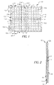
- FIG. 1 shows a display 10 in accordance with the present invention that has four aligned tiles 12a-12d, respectively.
- two or more tiles aligned along at least one edge are necessary.
- Each of the tiles is aligned along one edge of each of the tiles but are spaced from each other. This is clearly shown in FIG. 1 where the edge 12a' and 12a" are aligned with respect to edges 12b' and 12c' of tiles 12b and 12c, respectively.
- each tile has electric field activatable pixels p which produce light and such pixels being spaced from their aligned edge.
- the aligned edges be parallel, it will be understood that they can be slightly out of parallel as long as the pixels on the tiles line up to produce a seamless image as will be subsequently described.
- the display 10 includes a back plate 14 aligned with the four tiles 12a-12d and having electric field activatable pixels p' which are disposed so that they are positioned in the space provided between the aligned tiles 12a-12d whereby, when pixels p on the four tiles 12a-12d and the back plate 14 are activated, a seamless image is produced.
- the back plate 14 is aligned with the four tiles 12a-12d and having electric field activatable pixels p' which are disposed so that they are positioned in the space provided between the aligned tiles whereby, when pixels p on the four tiles 12a-12d and the back plate 14 are activated, a seamless image is produced.
- the tiles 12a-12d are affixed to the back plate 14 along the perimeter by adhesive or other bonding means.
- the tiles 12a-12d are positioned between the back plate 14 and a front plate 16.
- the tiles 12a-12d can be affixed to either the back plate 14 or front plate 16.
- the back plate 14 and front plate 16 are sealed around the perimeter enclosing the tile array within.
- a desiccant may also be positioned in or near any of the seals previously described.
- An oxygen getter can be disposed in or near any of the seals previously described.
- a polarization film 18 can be attached to the back plate 14 or the front plate 16 as needed to increase the contrast ratio of the tiled display 10.
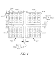
- Equal pixel to pixel pitches in the x and y direction px and py, respectively, and equal pixel edge to adjacent pixel edge spacing in the x and y direction spx and spy, respectively, are shown in FIGS. 1, 3, and 4 for both the tiles and the back plate.
- the terms "spx" and “spy” refer to the spacing between pixels on a tile in the x and y direction, respectively.
- the tile edge pixel to an adjacent tiled edge pixel in an adjacent tile is shown in the x and y directions as 3px and 3py.
- the ranges of allowable gap spacing in the x and y direction between adjacent tiles 0 px to (2 px + spx) and 0 py (2py + spy), respectively, are shown in FIG. 4.
- the tiled pixels can include different dyes to produce different colors. These tiled color pixels can be patterned to form a completely colored image when viewed by a user and each one of them is individually addressable. Typical color combinations are red, green, and blue.
- FIGS. 5, 6, and 7 describe examples of tiles that have organic electroluminescent materials.
- a light-emitting layer of an organic EL tile comprises a luminescent or fluorescent material where electroluminescence is produced as a result of electron-hole pair recombination in this region.
- a light-emitting layer 108 is sandwiched between anode 104 and cathode 106.
- the light-emitting layer 108 is a pure material with a high luminescent efficiency.
- a well known material is tris (8-quinolinato) aluminum, (Alq), which produces excellent green electroluminescence.
- the simple structure can be modified to a multilayer structure in which an additional electroluminescent layer is introduced between the hole and electron-transporting layers to function primarily as the site for hole-electron recombination and thus electroluminescence.
- the functions of the individual organic layers are distinct and can therefore be optimized independently.
- the electroluminescent or recombination layer can be chosen to have a desirable EL color as well as high luminance efficiency.
- the electron and hole transport layers can be optimized primarily for the carrier transport property.
- a multilayer organic light-emitting device 200 has a light-transmissive substrate 202 on which is disposed a light-transmissive anode 204.
- the anode 204 comprises two layers 204a and 204b.
- An organic light-emitting structure 208 is formed between the anode 204 and a cathode 206.
- the organic light-emitting structure 208 is comprised of, in sequence, an organic hole-transporting layer 210, an organic light-emitting layer 212, and an organic electron-transporting layer 214.
- the cathode 206 When an electrical potential difference (not shown) is applied between the anode 204 and the cathode 206, the cathode 206 will inject electrons into the electron-transporting layer 214, and the electrons will migrate across layer 214 to the light-emitting layer 212. At the same time, holes will be injected from the anode 204 into the hole-transporting layer 210. The holes will migrate across layer 210 and recombine with electrons at or near a junction formed between the hole-transporting layer 210 and the light-emitting layer 212. When a migrating electron drops from its conduction band to a valance band in filling a hole, energy is released as light, and is emitted through the light-transmissive anode 204 and substrate 202.
- the organic EL devices can be viewed as a diode, which is forward biased when the anode is at a higher potential than the cathode.
- the anode and cathode of the organic EL device can each take any convenient conventional form, such as any of the various forms disclosed by Tang and others in US-A-4,885,211. Operating voltage can be substantially reduced when using a low-work function cathode and a high-work function anode.
- the preferred cathodes are those constructed of a combination of a metal having a work function less than 4.0 eV and one other metal, preferably a metal having a work function greater than 4.0 eV.
- the Mg: Ag of Tang and others in US-A-4,885,211 constitutes one preferred cathode construction.
- the Al:Mg cathodes of Van Slyke and others in US-A-5,059,062 is another preferred cathode construction. Hung and others in US-A-5,776,622 has disclosed the use of a if/Al bilayer to enhanced electron injection in organic EL devices.
- Conventional anodes 204a are formed of a conductive and transparent oxide. Indium tin oxide has been widely used as the anode contact because of its transparency, good conductivity, and high work function.
- a multilayer organic device 300 emitting light from the top has a substrate 302 on which is disposed a light reflective conductive anode 304.
- the anode 304 comprises two layers including a light reflective conductive metal layer 304a and a thin transparent layer of a conductive high work function material 304b.
- An organic light-emitting structure 308 is formed between the anode 304 and a cathode 306.
- the cathode 306 is composed of two layers including a thin transparent conductive layer of a low work function material 306a and a transparent conductive layer such as indium tin oxide 306b.
- the organic light-emitting structure 308 is comprised of, in sequence, an organic hole-transporting layer 310, an organic light-emitting layer 312, and an organic electron-transporting layer 314.
- an electrical potential difference (not shown) is applied between the anode 304 and the cathode 306, the cathode will inject electrons into the electron-transporting layer 314, and the electrons will migrate across layer 314 to the light-emitting layer 312.
- holes will be injected from the anode 304 into the hole-transporting layer 310.
- the holes will migrate across layer 310 and recombine with electrons at or near a junction formed between the hole-transporting layer 310 and the light-emitting layer 312.
- a migrating electron drops from its conduction band to a valence band in filling a hole, energy is released as light, and is emitted through the light-transmissive cathode 306.
Landscapes
- Devices For Indicating Variable Information By Combining Individual Elements (AREA)
- Electroluminescent Light Sources (AREA)
- Transforming Electric Information Into Light Information (AREA)
Abstract
Description
Claims (7)
- A display, comprising:a) at least two tiles which are aligned along one edge of each tile but are spaced from each other, each tile having electric field activatable pixels which produce light, each tile having said pixels spaced from their aligned edge; andb) a back plate aligned with the two tiles and having electric field activatable pixels which are disposed so that they are positioned in the space provided between the aligned tiles whereby, when pixels on the two tiles and the back plate are activated, a seamless image is produced.
- The display of claim 1 wherein there are four tiles aligned in a rectangle so that each tile has two aligned edges which are spaced from adjacent tiles and wherein the back plate includes field activatable pixels positioned in the space between aligned tiles.
- The display of claim 2 wherein the pixels in the four aligned tiles are electroluminescent pixels which are individually addressable.
- The display of claim 2 wherein the pixels in each tile are arranged in columns and rows and having the same predetermined pitch between columns and rows, respectively, and wherein the pixels in the back plate have the same pitch corresponding to rows and columns so that a seamless image is produced.
- The display of claim 4 wherein an image is produced that can be viewed from the front or back side of the display.
- The display of claim 3 wherein the pixels on the tiles are arranged as an active matrix and the pixels on the back plate are arranged as a passive matrix.
- The display of claim 5 wherein a polarization layer is provided over the side of the viewed display.
Applications Claiming Priority (2)
| Application Number | Priority Date | Filing Date | Title |
|---|---|---|---|
| US757921 | 2001-01-10 | ||
| US09/757,921 US6614171B2 (en) | 2001-01-10 | 2001-01-10 | Light-producing display having spaced apart tiles |
Publications (2)
| Publication Number | Publication Date |
|---|---|
| EP1223458A2 true EP1223458A2 (en) | 2002-07-17 |
| EP1223458A3 EP1223458A3 (en) | 2003-07-23 |
Family
ID=25049755
Family Applications (1)
| Application Number | Title | Priority Date | Filing Date |
|---|---|---|---|
| EP02075008A Withdrawn EP1223458A3 (en) | 2001-01-10 | 2002-01-02 | Tiled display |
Country Status (3)
| Country | Link |
|---|---|
| US (1) | US6614171B2 (en) |
| EP (1) | EP1223458A3 (en) |
| JP (1) | JP2002304135A (en) |
Cited By (3)
| Publication number | Priority date | Publication date | Assignee | Title |
|---|---|---|---|---|
| WO2006057801A3 (en) * | 2004-11-23 | 2006-11-09 | Eastman Kodak Co | Tiled oled display |
| US7190390B2 (en) * | 2000-07-10 | 2007-03-13 | Honeywell International, Inc. | LCD tile display |
| US7394194B2 (en) * | 2004-11-23 | 2008-07-01 | Eastman Kodak Company | Tiled display |
Families Citing this family (16)
| Publication number | Priority date | Publication date | Assignee | Title |
|---|---|---|---|---|
| TW556447B (en) * | 2002-09-05 | 2003-10-01 | Au Optronics Corp | An organic light emitting diode |
| TW594201B (en) * | 2003-03-28 | 2004-06-21 | Toppoly Optoelectronics Corp | Reflective LCD having two driving matrixes |
| JP2005195999A (en) * | 2004-01-09 | 2005-07-21 | Seiko Instruments Inc | Liquid crystal display |
| TWI300863B (en) * | 2004-03-19 | 2008-09-11 | Toppoly Optoelectronics Corp | Transmissive liquid crystal display |
| KR101415571B1 (en) * | 2007-10-15 | 2014-07-07 | 삼성디스플레이 주식회사 | Display device and driving method of the same |
| US8179336B2 (en) * | 2008-06-30 | 2012-05-15 | Global Oled Technology, Llc. | Tiled electronic display |
| KR101045264B1 (en) * | 2008-09-09 | 2011-06-29 | 네오뷰코오롱 주식회사 | Display device, mobile device having same and display control method |
| KR101045265B1 (en) * | 2009-05-29 | 2011-06-29 | 네오뷰코오롱 주식회사 | Display device |
| US8305294B2 (en) | 2009-09-08 | 2012-11-06 | Global Oled Technology Llc | Tiled display with overlapping flexible substrates |
| US9111493B2 (en) | 2010-09-14 | 2015-08-18 | Sharp Kabushiki Kaisha | Display device |
| CN104361837A (en) * | 2014-11-20 | 2015-02-18 | 冠捷显示科技(中国)有限公司 | Tiled display screen and seamless display method thereof |
| KR102239170B1 (en) | 2015-01-29 | 2021-04-12 | 삼성디스플레이 주식회사 | Display device and method of manufacturing the same |
| KR102361711B1 (en) | 2015-02-02 | 2022-02-11 | 삼성디스플레이 주식회사 | Organic light emitting display device and method of manufacturing thereof |
| US10378704B2 (en) * | 2017-10-05 | 2019-08-13 | Christie Digital Systems Usa, Inc. | LED module seam illumination |
| TWI781241B (en) * | 2017-11-08 | 2022-10-21 | 美商康寧公司 | Apparatus and methods for assembling a display area |
| CN114120845B (en) * | 2021-11-30 | 2024-01-26 | 京东方科技集团股份有限公司 | Display modules and spliced display devices |
Family Cites Families (9)
| Publication number | Priority date | Publication date | Assignee | Title |
|---|---|---|---|---|
| US4885211A (en) | 1987-02-11 | 1989-12-05 | Eastman Kodak Company | Electroluminescent device with improved cathode |
| DE3910418A1 (en) | 1989-03-31 | 1990-10-04 | Licentia Gmbh | DISPLAY DEVICE |
| US5059062A (en) | 1990-06-14 | 1991-10-22 | Pat Bresnahan | Concrete path paver with removeable slip-forming screed |
| US5661531A (en) | 1996-01-29 | 1997-08-26 | Rainbow Displays Inc. | Tiled, flat-panel display having invisible seams |
| US5801797A (en) * | 1996-03-18 | 1998-09-01 | Kabushiki Kaisha Toshiba | Image display apparatus includes an opposite board sandwiched by array boards with end portions of the array boards being offset |
| US5776622A (en) | 1996-07-29 | 1998-07-07 | Eastman Kodak Company | Bilayer eletron-injeting electrode for use in an electroluminescent device |
| JPH10268332A (en) * | 1997-03-24 | 1998-10-09 | Sharp Corp | Liquid crystal display device and method of manufacturing the same |
| US5903328A (en) | 1997-06-16 | 1999-05-11 | Rainbow Displays, Inc. | Tiled flat-panel display with tile edges cut at an angle and tiles vertically shifted |
| JP3300638B2 (en) * | 1997-07-31 | 2002-07-08 | 株式会社東芝 | Liquid crystal display |
-
2001
- 2001-01-10 US US09/757,921 patent/US6614171B2/en not_active Expired - Lifetime
-
2002
- 2002-01-02 EP EP02075008A patent/EP1223458A3/en not_active Withdrawn
- 2002-01-08 JP JP2002001406A patent/JP2002304135A/en active Pending
Cited By (3)
| Publication number | Priority date | Publication date | Assignee | Title |
|---|---|---|---|---|
| US7190390B2 (en) * | 2000-07-10 | 2007-03-13 | Honeywell International, Inc. | LCD tile display |
| WO2006057801A3 (en) * | 2004-11-23 | 2006-11-09 | Eastman Kodak Co | Tiled oled display |
| US7394194B2 (en) * | 2004-11-23 | 2008-07-01 | Eastman Kodak Company | Tiled display |
Also Published As
| Publication number | Publication date |
|---|---|
| US6614171B2 (en) | 2003-09-02 |
| US20020130987A1 (en) | 2002-09-19 |
| EP1223458A3 (en) | 2003-07-23 |
| JP2002304135A (en) | 2002-10-18 |
Similar Documents
| Publication | Publication Date | Title |
|---|---|---|
| US6614171B2 (en) | Light-producing display having spaced apart tiles | |
| US11631721B2 (en) | Organic light emitting display device having a plurality of green sub pixels disposed between at least one red sub pixel and at least one blue sub pixel | |
| KR101994816B1 (en) | Transparent organic light emitting diodes | |
| US6853411B2 (en) | Light-producing high aperture ratio display having aligned tiles | |
| US11063244B2 (en) | Electroluminescent display device | |
| US6580214B2 (en) | Color display apparatus having electroluminescence elements | |
| US8305294B2 (en) | Tiled display with overlapping flexible substrates | |
| US20080036376A1 (en) | Organic electroluminescence display panel and method for sealing the same | |
| JP3234936B2 (en) | Organic light emitting device and image display device | |
| US9960211B2 (en) | Pixel element structure, array structure and display device | |
| KR20130093187A (en) | Organic light emitting display device and method for manufacturing thereof | |
| KR101901350B1 (en) | Organic light emitting display device | |
| JP3852518B2 (en) | Organic electroluminescence device | |
| JP3820752B2 (en) | Organic electroluminescence device | |
| JP3852517B2 (en) | Organic electroluminescence device | |
| KR20000073118A (en) | Organic electroluminescent display device | |
| JP4185371B2 (en) | Stereoscopic image display device | |
| CN110611046B (en) | Double-sided display panel | |
| KR100712122B1 (en) | Flat Panel Display | |
| JP3852520B2 (en) | Organic electroluminescence device | |
| KR100779943B1 (en) | Organic light emitting device | |
| JP2000123980A (en) | Light emitting device and method of manufacturing the same | |
| KR100710733B1 (en) | Organic electroluminescent element provided with photoluminescence layer, organic electroluminescent display panel | |
| KR20260004656A (en) | Display device | |
| KR100934261B1 (en) | Organic light emitting display device |
Legal Events
| Date | Code | Title | Description |
|---|---|---|---|
| PUAI | Public reference made under article 153(3) epc to a published international application that has entered the european phase |
Free format text: ORIGINAL CODE: 0009012 |
|
| AK | Designated contracting states |
Kind code of ref document: A2 Designated state(s): AT BE CH CY DE DK ES FI FR GB GR IE IT LI LU MC NL PT SE TR |
|
| AX | Request for extension of the european patent |
Free format text: AL;LT;LV;MK;RO;SI |
|
| PUAL | Search report despatched |
Free format text: ORIGINAL CODE: 0009013 |
|
| AK | Designated contracting states |
Designated state(s): AT BE CH CY DE DK ES FI FR GB GR IE IT LI LU MC NL PT SE TR |
|
| AX | Request for extension of the european patent |
Extension state: AL LT LV MK RO SI |
|
| RIC1 | Information provided on ipc code assigned before grant |
Ipc: 7H 01L 27/00 B Ipc: 7G 02F 1/1347 B Ipc: 7H 01L 51/20 B Ipc: 7G 02F 1/1333 A |
|
| 17P | Request for examination filed |
Effective date: 20031210 |
|
| AKX | Designation fees paid |
Designated state(s): DE FR GB |
|
| STAA | Information on the status of an ep patent application or granted ep patent |
Free format text: STATUS: THE APPLICATION IS DEEMED TO BE WITHDRAWN |
|
| 18D | Application deemed to be withdrawn |
Effective date: 20080801 |