Technical Field
-
The present invention relates to an apparatus for and a method of
separating substances such as organic molecules charged in a solution, and
more particularly, it relates to a separation apparatus and a separation
method applied to crystallization of organic polymers including various
biopolymers such as protein, enzyme etc. and complexes thereof. Further,
the present invention relates to an apparatus and a method for preparing a
crystal of a polymer and a kit for the apparatus, and more particularly, it
relates to an apparatus, a method and a kit applied to crystallization of
polymers including various biopolymers such as protein, enzyme etc. and
complexes thereof.
Background Art
-
Crystallization of a biopolymer such as protein is basically performed
by eliminating a solvent from water or a nonaqueous solution containing
the polymer for supersaturating the biopolymer and growing a crystal,
similarly to the case of a general low molecular weight compound such as
inorganic salt. Typical methods for such crystallization include a batch
method, dialysis and vapor diffusion, which are selectively used in response
to the type, quantity, property etc. of a sample.
-
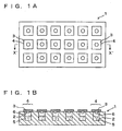
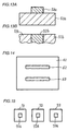
Figs. 1A and 1B show an apparatus 1 for trying crystallization by
vapor deposition under various conditions. The apparatus 1 has a number
of wells 2, so that each well 2 and each plate 3 form a cell 4 for
crystallization. Each well 2 holds a precipitant 5, while a mother liquor 6
containing a biopolymer to be crystallized is dropped onto each plate 3
blocking an opening of the well 2. In this apparatus 1, equilibrium is set
up due to evaporation of volatile components contained in the precipitant 5
and the mother liquor 6.
-
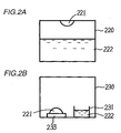
Figs. 2A and 2B schematically show a hanging-drop method and a
sitting-drop method included in vapor diffusion respectively. In the
hanging-drop method shown in Fig. 2A, a mother liquor 221 containing a
biopolymer to be crystallized is dropped in a closed vessel 220 storing a
precipitant 222. In the sitting-drop method shown in Fig. 2B, a mother
liquor 221 containing a biopolymer to be crystallized is placed on a plate
233 in a closed vessel 230. A precipitant 222 is stored in another vessel
231 in the closed vessel 230. According to these methods, equilibrium is
loosely set up due to evaporation of volatile components contained in the
precipitants and the mother liquors.
-
In order to decide the three-dimensional structure of a biopolymer by
X-ray crystallographic analysis, the target substance must be extracted,
purified and thereafter crystallized. According to a conventional method,
the operator progresses crystallization while repeating trial and error based
on his intuition and experience. In this case, research must be made
under an extremely large number of experimental conditions for obtaining
a crystal of the biopolymer, and crystal growth is regarded as the largest
bottleneck in the field of X-ray crystallographic analysis.
-
As a new method substituting for the conventional method or a
method for more efficiently growing a crystal in combination with the
conventional method, a method of and an apparatus for performing
crystallization with a semiconductor substrate having controlled valence
electrons or the like (refer to International Patent Laying-Open Nos.
WO96/26781, WO97/49845, WO98/02601 and WO99/23284). According to
this method, a crystal nucleus can be fixed to the surface of a solid-state
component brought into a prescribed electric state by valence control due to
electrostatic action. A compound such as protein flocculates on the surface
of the solid-state component due to electrostatic interaction so that
formation of a crystal nucleus can be prompted for bringing growth of a
crystal. Crystallization can be controlled by controlling electric
characteristics on the surface of the solid-state component.
-
A crystal of a biopolymer generally contains a large quantity (≧ 50
volume %, for example) of solvent, dissimilarly to other substances. When
such a crystal is left in the air, the solvent is scattered to break the crystal.
In order to prevent this, the crystal is generally sealed in a glass capillary
along with a mother liquor, and subjected to an X-ray crystallographic
analysis experiment under the atmosphere of the mother liquor having
concentration and pH at equilibrium. Recently, a technique, referred to as
flash cooling, of instantaneously freezing a biopolymer crystal with liquid
nitrogen or the like may be employed for performing X-ray crystallographic
analysis while keeping a solvent contained in the crystal in a glass state.
Anyway, it is important to grow a crystal of a sufficient size from a mother
liquor, to be subjected to X-ray crystallographic analysis with no breakage.
Disclosure of the Invention
-
An object of the present invention is to technically solve problems of
a conventional crystallization process progressed while repeating trial and
error.
-
Another object of the present invention is to provide an apparatus
and a method capable of flocculating and adsorbing a biopolymer contained
in a solution to a specific region of a solid surface with electrostatic action.
-
More specifically, the object of the present invention is to provide a
technique of reducing influence by convection in a solution influenced by
gravity and controlling nucleation in crystallization of various biopolymers
and a vital tissue mainly formed by biopolymers.
-
Still another object of the present invention is to provide a technique
capable of obtaining a large-sized crystal capable of enabling X-ray
crystallographic analysis by suppressing or controlling mass generation of
microcrystals.
-
A further object of the present invention is to provide a technique for
enabling crystallization with a small quantity of biopolymer solution.
-
A further object of the present invention is to provide a method of
and an apparatus for enabling crystallization with a small quantity of
solution.
-
A further object of the present invention is to provide an apparatus
and a method capable of readily taking out a generated crystal without
breaking the same.
-
A further object of the present invention is to technically solve
problems in a process of taking out a crystal in a technique of growing a
crystal of a biopolymer such as protein on a solid surface.
-
A further object of the present invention is to provide a technique
capable of readily finding conditions suitable for crystallization.
-
In particular, a further object of the present invention is to provide a
novel screening apparatus and a novel screening method capable of
bringing conditions suitable for crystallization or flocculation of various
polymers in a shorter time.
-
According to an aspect of the present invention, an apparatus for
separating a charged substance contained in a solution from the solution
comprises a plurality of types of solids consisting of materials substantially
different from each other selected from a group consisting of a metal, a
semiconductor and a compound thereof. In this apparatus, the surfaces of
the plurality of types of solids are arranged to simultaneously come into
contact with the solution, and the surfaces of the plurality of types of solids
have surface potentials or zeta potentials different from each other when
coming into contact with the solution, thereby more strongly
electrostatically adsorbing the substance to the surface of any of the
plurality of types of solids.
-
In the apparatus according to the present invention, at least one of
the plurality of types of solids may have a porous surface. The surface of
the solid having the porous surface can have a surface potential or a zeta
potential different from those of the surfaces of the remaining solids, so
that the substance can be more strongly electrostatically adsorbed to the
porous surface. Preferably, the porous surface mainly has pores having a
pore diameter substantially equivalent to or not more than the size of the
substance to be separated. Preferably, the material for the solid having
the porous surface is alumina.
-
The apparatus according to the present invention preferably further
comprises an enclosure wall for holding the solution on the surfaces of the
plurality of types of solids.
-
In a preferred mode of the present invention, the plurality of types of
solids are arranged to be adjacent to each other in a prescribed region, and
the area occupied by the surface of the solid more strongly electrostatically
adsorbing the substance is not more than the area occupied by the surfaces
of the remaining solids in the prescribed region.
-
In the apparatus according to the present invention, the plurality of
types of solids can be formed on the same substrate. The substrate can be
a semiconductor substrate.
-
In the apparatus according to the present invention, the materials
providing the plurality of types of solids can have a multilayer structure,
and the upper layer material can be provided on a plurality of positions on
the lower layer material at intervals.
-
According to another aspect of the present invention, an apparatus
for separating a charged substance contained in a solution from the
solution has a surface for coming into contact with the solution, the surface
has a plurality of regions, the respective ones of the plurality of regions are
surfaces exposing materials substantially different from each other selected
from a group consisting of a metal, a semiconductor and a compound
thereof, the plurality of regions are charged to surface potentials different
from each other when coming into contact with the solution, and one of
plurality of regions electrostatically adsorbs the charged substance more
strongly than the others of the plurality of regions.
-
According to still another aspect of the present invention, an
apparatus for separating a charged substance contained in a solution from
the solution comprises a first solid and a second solid, wherein the first
solid is a semiconductor substrate and the second solid is an island made of
a semiconductor compound or an island made of a metal compound formed
on the first solid. The surface of the first solid and the surface of the
second solid are charged to surface potentials or zeta potentials different
from each other when coming into contact with the solution, thereby the
surface of the second solid electrostatically adsorbs the charged substance
more strongly. Preferably, the semiconductor substrate is a silicon
substrate. The material for at least the top portion of the island can be
any of a silicon oxide, a silicon nitride, a metal oxide and a metal nitride.
The width of the top portion of the island is preferably 10 µm to 200 µm.
The apparatus can have an enclosure wall for holding the solution,
provided on the surface of the first solid to enclose the island. Preferably,
the first solid and the second solid are arranged to be adjacent to each other
in a region enclosed with the enclosure wall, and the area of the surface of
the top portion of the second solid is smaller than the area of the surface of
the first solid in this region. The second solid can be a plurality of islands
having different widths of top portions. For example, the combination of
the material for the surface part of the first solid and the material for the
surface part of the second solid is a combination of any of silicon and a
silicon oxide, silicon and a silicon nitride, and silicon and alumina.
-
According to a further aspect of the present invention, an apparatus
for separating a charged substance contained in a solution from the
solution comprises a semiconductor substrate, a first solid and a second
solid, the first solid is a semiconductor compound film or a metal compound
film formed on the semiconductor substrate, and the second solid is an
island made of a semiconductor compound or an island made of a metal
compound formed on the first solid. The surface of the first solid and the
surface of the second solid are charged to surface potentials or zeta
potentials different from each other when coming into contact with the
solution, thereby the surface of the second solid electrostatically adsorbs
the charged substance more strongly. Preferably, the semiconductor
substrate is a silicon substrate. For example, the material for at least the
top portion of the island is any of a silicon oxide, a silicon nitride, a metal
oxide and a metal nitride. The width of the top portion of the island is
preferably 10 µm to 200 µm. The apparatus can have an enclosure wall
for holding the solution, provided on the surface of the first solid to enclose
the island. Preferably, the first solid and the second solid are arranged to
be adjacent to each other in a region enclosed with the enclosure wall, and
the area of the surface of the top portion of the second solid is smaller than
the area of the surface of the first solid in this region. The second solid
can be a plurality of islands having different widths of top portions. For
example, the combination of the material for the surface part of the first
solid and the material for the surface part of the second solid is a
combination of any of a silicon oxide and a silicon nitride, a silicon oxide
and alumina, and a silicon nitride and alumina.
-
According to a further aspect of the present invention, an apparatus
for separating a charged substance contained in a solution from the
solution comprises a first member having a plurality of through holes
provided at spaces from each other and a second member combined with
the first member to block the plurality of through holes. A surface of the
second member exposed in the through holes includes a first region and a
second region. The first region and the second region are charged to
surface potentials or zeta potentials different from each other when the
surface comes into contact with the solution, thereby the second region
electrostatically adsorbs the charged substance more strongly.
-
In the present invention, the first region can be a surface exposing a
first material selected from a group consisting of a metal, a semiconductor
and a compound thereof, and the second region can be a surface exposing a
material selected from a group consisting of a metal, a semiconductor and a
compound thereof substantially different from the first material. Typically,
the first material is a material selected from a group consisting of silicon, a
silicon oxide film and a silicon nitride film, and the second material is a
material selected from a group consisting of silicon, a silicon nitride and a
metal oxide film. In the apparatus, a plurality of second members can be
provided, so that the single first member and the plurality of second
members can be combined with each other.
-
In the present invention, the first region can be a surface exposing a
first material selected from a group consisting of a metal, a semiconductor
and a compound thereof, and the second region can be a surface exposing a
material substantially different from the first material. Combinations of
the first material and the second material may be different from each other
between the plurality of second members.
-
Preferably, the second region is smaller than the first region.
-
The apparatus according to the present invention can further
comprise means for measuring the pH of the solution containing the
substance. Preferably, the pH measuring means includes a semiconductor
layer, an insulating layer formed on the semiconductor layer, an enclosure
wall for holding the solution on the insulating layer and a metal electrode
provided on the enclosure wall to come into contact with the solution.
-
Typically, the charged substance is an organic molecule in the
present invention. Typically, the organic molecule is a biopolymer.
Typically, the biopolymer is protein.
-
Typically, the apparatus according to the present invention is
employed for preparing a crystal of the organic molecule.
-
According to a further aspect of the present invention, a method of
separating a charged organic molecule contained in a solution from the
solution comprises a step of bringing the solution containing the organic
molecule and having pH other than the isoelectric point of the organic
molecule into contact with the surfaces of the plurality of types of solids of
the aforementioned apparatus.
-
According to a further aspect of the present invention, a method of
separating a charged organic molecule contained in a solution from the
solution comprises steps of bringing the solution containing the organic
molecule and having pH other than the isoelectric point of the organic
molecule into contact with the surfaces of the plurality of types of solids of
the aforementioned apparatus and maintaining the contact so that a crystal
of the organic molecule grows on any of the surfaces of the plurality of types
of solids.
-
According to a further aspect of the present invention, a method of
preparing a crystal comprises steps of bringing a solution containing an
organic molecule and having pH other than the isoelectric point of the
organic molecule into contact with the surfaces of the plurality of types of
solids of the aforementioned apparatus, and sealing the apparatus along
with a precipitant and maintaining the contact so that the crystal of the
organic molecule grows on any of the surfaces of the plurality of types of
solids.
-
In the method according to the present invention, the pH of the
solution containing the organic molecule brings a surface potential or a zeta
potential of a reverse polarity to the organic molecule to at least one of the
surfaces of the plurality of types of solids while bringing a surface potential
or a zeta potential of the same polarity as the organic molecule to the
surfaces of the remaining solids.
-
According to a further aspect of the present invention, a kit for the
aforementioned apparatus comprises a first member having a plurality of
through holes provided at spaces from each other, and a plurality of second
members having a plurality of types of surfaces exhibiting surface
potentials or zeta potentials different from each other in the solution
respectively.
-
According to a further aspect of the present invention, an apparatus
for preparing a crystal of protein contained in a solution comprises a
substrate and an island, formed on a prescribed region of the substrate,
consisting of a material substantially different from the substrate at least
on a top portion, wherein the surface of the substrate and the surface of the
island are charged to surface potentials different from each other when the
island and the surface of the substrate present around the island are
simultaneously brought into contact with the solution, thereby the island
adsorbs a protein molecule contained in the solution and the crystal of
protein growths on the island. The apparatus can have an enclosure wall
provided on the substrate to enclose the island and the surface of the
substrate present around the island. Preferably, the area occupied by the
surface of the top portion of the island present on a portion enclosed with
the enclosure wall is smaller than the area occupied by the surface of the
substrate other than the island present on the portion. The top portion of
the island preferably has a width allowing the crystal of protein to grow
beyond the top portion of the island. For example, the width of the top
portion of the island is 10 µm to 200 µm.
-
According to a further aspect of the present invention, an apparatus
for preparing a crystal of protein contained in a solution comprises a
substrate, a film formed on the substrate and an island, formed on the film,
consisting of a material substantially different from the film at least on a
top portion, wherein the surface of the film and the surface of the island are
charged to surface potentials different from each other when the island and
the surface of the film present around the island are simultaneously
brought into contact with the solution, thereby the island adsorbs a protein
molecule contained in the solution and the crystal of protein growths on the
island. The apparatus can further comprise an enclosure wall provided on
the substrate to enclose the island and the surface of the film present
around the island. Preferably, the area occupied by the surface of the top
portion of the island present on a portion enclosed with the enclosure wall
is smaller than the area occupied by the surface of the substrate other than
the island present on the portion. The top portion of the island preferably
has a width allowing the crystal of protein to grow beyond the top portion of
the island. For example, the width of the top portion of the island is 10 µm
to 200 µm.
-
According to a further aspect of the present invention, an apparatus
for preparing a crystal of an organic molecule contained in a solution
comprises (1) a first member having a plurality of through holes provided
at spaces from each other and (2) a plurality of second members bonded to
the first member, while the second members include (a) substrates and (b)
islands, formed on the surfaces of the substrates, consisting of a material
different from the substrates at least on top portions. The islands are
formed to be present inside the through holes. Preferably, the substrates
consist of silicon, and the material for at least the top portions of the
islands consists of a metal oxide or a silicon nitride.
-
According to a further aspect of the present invention, an apparatus
for preparing a crystal of an organic molecule contained in a solution
comprises (1) a first member having a plurality of through holes provided
at spaces from each other and (2) a plurality of second members bonded to
the first member, while the second members include (a) substrates, (b)
films, formed on the surfaces of the substrates, consisting of a material
different from the substrates, and (c) islands, formed on the films,
consisting of a material different from the films at least on top portions.
The islands are formed to be present inside the through holes. Preferably,
the substrates consist of silicon, and the material for at least the top
portions of the islands consists of a metal oxide or a silicon nitride.
Brief Description of the Drawings
-
- Fig. 1A is a plan view showing an exemplary conventional
crystallization apparatus employing vapor diffusion, and Fig. 1B is a
sectional view taken along the line X'-X' in Fig. 1A.
- Figs. 2A and 2B are schematic diagrams showing conventional
crystal growth.
- Fig. 3 is a schematic sectional view showing an exemplary apparatus
according to the present invention.
- Fig. 4 is a schematic sectional view showing another exemplary
apparatus according to the present invention.
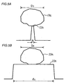
- Figs. 5A and 5B are schematic sectional views showing apparatuses
having different widths of adsorption surfaces supplied to islands
respectively.
- Figs. 6A and 6B are schematic diagrams showing organic molecules
adsorbed and fixed to porous solid surfaces in the apparatus according to
the present invention.
- Fig. 7 is a schematic diagram showing organic molecules adsorbed
and fixed to a porous solid surface in the apparatus according to the
present invention.
- Fig. 8 is a schematic diagram showing a method of anodization
employed for preparation of the apparatus according to the present
invention.
- Fig. 9 illustrates surface potentials of two types of solid surfaces and
a protein molecule contained in a solution varying with the pH of the
solution.
- Fig. 10 illustrates surface potentials of two types of solid surfaces
and a protein molecule contained in a solution varying with the pH of the
solution.
- Fig. 11 illustrates pH dependency of zeta potentials of some
substances.
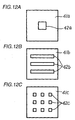
- Figs. 12A to 12C are plan views showing exemplary patterns on
which a plurality of solid surfaces are arranged in the apparatus according
to the present invention.
- Figs. 13A and 13B are sectional views showing exemplary patterns
on which a plurality of solid surfaces are arranged in the apparatus
according to the present invention.
- Fig. 14 is a plan view showing an exemplary apparatus having a
plurality of preferred adsorption surfaces according to the present
invention.
- Fig. 15 illustrates crystallization performed in a plurality of
apparatuses under different conditions according to the present invention.
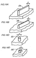
- Figs. 16A to 16D are perspective views schematically showing
various shapes of islands.
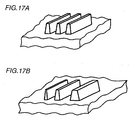
- Figs. 17A and 17B are perspective views showing a part of the
apparatus provided with a plurality of islands.
- Fig. 18A is a sectional view showing still another exemplary
apparatus according to the present invention, and Fig. 18B is a plan view
thereof.
- Figs. 19A to 19D are schematic sectional views illustrating a method
of manufacturing the apparatus shown in Figs. 18A and 18B.
- Fig. 20A is a sectional view showing a further exemplary apparatus
according to the present invention, and Fig. 20B is a plan view thereof.
- Figs. 21A to 21D are schematic sectional views illustrating a method
of manufacturing the apparatus shown in Figs. 20A and 20B.
- Fig. 22A is a sectional view showing a further exemplary apparatus
according to the present invention, and Fig. 22B is a plan view thereof.
- Figs. 23A to 23D are schematic sectional views illustrating a method
of manufacturing the apparatus shown in Figs. 22A and 22B.
- Figs. 24A to 24D are schematic sectional views illustrating another
method of manufacturing the apparatus according to the present invention.
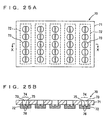
- Fig. 25A is a plan view showing an exemplary crystal preparation
apparatus according to the present invention, and Fig. 25B is a sectional
view taken along the line X-X in Fig. 25A.
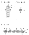
- Fig. 26A is a plan view showing a second substrate shown in Figs.
25A and 25B, and Fig. 26B is a sectional view taken along the line Y-Y in
Fig. 26A.
- Fig. 27 is a sectional view showing a solution, containing a polymer
to be crystallized, held in the apparatus shown in Figs. 25A and 25B.
- Figs. 28A to 28E are sectional views schematically showing
exemplary structures of the second substrate used in the apparatus shown
in Figs. 25A and 25B respectively.
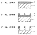
- Figs. 29A to 29C are schematic sectional views showing steps for
manufacturing the substrates shown in Figs. 28A to 28E.
- Figs. 30A to 30E are sectional views schematically showing specific
crystallization members used for the apparatus according to the present
invention.
- Fig. 31A is a plan view showing another exemplary second substrate
according to the present invention, and Fig. 31B is a sectional view showing
another exemplary apparatus formed by combining a first substrate and
the second substrate according to the present invention.
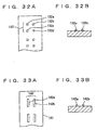
- Fig. 32A is a plan view showing exemplary surface arrangement in a
crystallization region, and Fig. 32B is a sectional view thereof.
- Fig. 33A is a plan view showing another exemplary surface
arrangement in a crystallization region, and Fig. 33B is a sectional view
thereof.
- Fig. 34A is a plan view showing a further exemplary apparatus
according to the present invention, and Fig. 34B is a sectional view taken
along the line Z-Z in Fig. 34A.
- Fig. 35 is a plan view of a second substrate shown in Figs. 33A and
33B.
- Fig. 36 is a sectional view showing a solution containing a polymer
held in the apparatus shown in Figs. 33A and 33B.
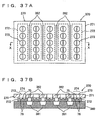
- Fig. 37A is a plan view showing an apparatus combined with a
substrate for holding a precipitant, and Fig. 37B is a sectional view thereof.
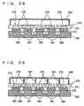
- Fig. 38 is a sectional view showing a mode of employment of the
apparatus shown in Figs. 37A and 37B.
- Fig. 39 is a sectional view showing another mode of employment of
the apparatus shown in Figs. 37A and 37B.
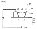
- Fig. 40 is a schematic sectional view showing an exemplary pH
sensor provided on the apparatus according to the present invention.
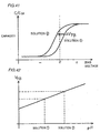
- Fig. 41 illustrates exemplary capacity-voltage characteristics
measured with the pH sensor shown in Fig. 40.
- Fig. 42 illustrates the relation between flat band potentials obtained
from the capacity-voltage characteristics measured with the pH sensor
shown in Fig. 40 and the pH values of solutions.
- Fig. 43 is a schematic diagram showing a flow of pH measurement in
the apparatus according to the present invention.
- Fig. 44 is a perspective view showing a further exemplary apparatus
according to the present invention.
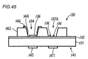
- Fig. 45 is a sectional view of the apparatus shown in Fig. 44.
- Fig. 46 is a sectional view showing an electrode in the apparatus
shown in Fig. 44 in an enlarged manner.
- Figs. 47A and 47B are plan views showing the patterns of islands
provided in crystal growth cells in the apparatus shown in Fig. 44 in an
enlarged manner.
- Fig. 48 is a perspective view showing the structure of a heating
element provided in the apparatus shown in Fig. 44 in an enlarged manner.
- Figs. 49A to 49E are schematic sectional views showing a method of
manufacturing a base portion of the apparatus shown in Fig. 44.
- Figs. 50A to 50F are schematic sectional views showing a method of
manufacturing a solution holding plate of the apparatus shown in Fig. 44.
- Fig. 51 is a schematic diagram showing another flow of pH
measurement in the apparatus according to the present invention.
- Fig. 52 is a plan view showing a further exemplary apparatus
according to the present invention.
- Figs. 53A to 53F are schematic sectional views showing a method of
manufacturing a base, having a porous surface, of the apparatus according
to the present invention.
- Figs. 54A to 54F are schematic sectional views showing a method of
manufacturing a solution holding plate combined with the base formed
through the process of Figs. 53A to 53F.
-
Best Mode for Carrying Out the Invention
-
In a general biopolymer such as protein, intermolecular recognition
is made by a geometrically specific structure and electrostatic interaction
(electrostatic repulsion/attraction or van der Waals force) in a solution. In
the intermolecular interaction based on electrostatic energy, it is predicted
that slight difference between spatial charge distributions on the outermost
surfaces of individual molecules exerts decisive influence on the degree of
intermolecular recognition and easiness in formation of a molecular
aggregate. In individual molecules repeating collision while making
Brownian motion in the solution, therefore, it is conceivable that a nucleus
of a molecular aggregate having a periodic and regular structure is
extremely hard to form.
-
In relation to formation of a crystal of protein molecules, it is
reported that the initial process of nucleation is important. When some
conditions for two-dimensionally arranging molecules forming a nucleus in
the initial process of crystallization are adjusted, subsequent crystallization
conceivably epitaxially progresses from this nucleus.
-
An apparatus and a method according to the present invention can
selectively adsorb organic molecules charged in a solution to a specific
region of the apparatus on the basis of a working mechanism described
below. Consequently, a crystal nucleus is formed on the specific region, to
be capable of bringing preferable crystal growth.
-
As shown in Fig. 3, an apparatus 10 according to the present
invention includes a first solid 11 having a first surface 11a and a second
solid 12 having a second surface 12a. The first solid 11 and the second
solid 12 consist of substantially different materials. In this case, the
wording "substantially different" means that the main materials forming
the solids are different from each other. The materials forming the solids
are metals, semiconductors or compounds thereof such as oxides,
hydroxides, nitrides or the like, for example. The apparatus 10 is brought
into contact with a solution 14 containing organic molecules 13 of protein or
the like to be separated or crystallized. The surfaces of the organic
molecules 13 are generally positively or negatively charged in a solution
having pH other than the isoelectric point of the molecules when
macroscopically observing the whole molecules. In the apparatus
according to the present invention, the solid surfaces 11a and 12a of the
aforementioned materials are also charged in the solution 14. At this time,
the values and polarities of the potentials of the surfaces of the solids
depend on the materials of the solids and the pH of the solution. For
example, the solid surface 11a is negatively charged and the solid surface
12a is positively charged in a solution of certain pH. On the other hand,
the organic molecules 13 are negatively charged in the solution of this pH.
In this case, the organic molecules 13 contained in the solution 14 are
selectively adsorbed to the solid surface 12a charged in the reverse polarity
to the organic molecules 13 according to electrostatic attraction.
Adsorption to the solid surface 11a charged in the same polarity as the
organic molecules 13 is inhibited by electrostatic action. Thus, separation
of the organic molecules 13 on the solid surface 12a is progressed, and
preferably a crystal nucleus of the organic molecules 13 is formed for
prompting crystallization. Thus, when a plurality of types of solids having
different surface potentials or zeta potentials are provided in a solution
containing charged organic molecules, the organic molecules can be
selectively adsorbed onto the surface of any solid. Consequently, a crystal
nucleus is formed on the surface of this solid, so that crystallization can be
selectively progressed.
-
As shown in Fig. 4, another apparatus 10 according to the present
invention may include a first solid 11 having a first surface 11a and an
island-shaped (or convex) second solid 12 having a second surface 12a.
The first solid 11 and the second solid 12 may consist of substantially
different materials, or may contain a common main material. In this case,
the wording "substantially different" means that the main materials
forming the solids are different from each other. When both solids contain
a common main material, the quantities or types of secondary materials
such as impurities or minor components are generally different from each
other. The materials forming the solids are metals, semiconductors or
compounds thereof such as oxides, hydroxides, nitrides or the like, for
example. The apparatus 10 is brought into contact with a solution 14
containing organic molecules 13 of protein or the like to be crystallized.
The surfaces of the organic molecules 13 are generally positively or
negatively charged in a solution having pH other than the isoelectric point
of the molecules when macroscopically observing the whole molecules. In
the apparatus according to the present invention, the surfaces 11a and 12a
are also charged in the solution 14. At this time, the values and polarities
of the potentials of the surfaces depend on the materials of the solids and
the pH of the solution. For example, the solid surface 11a is negatively
charged, the solid surface 12a is positively charged and the organic
molecules 13 are negatively charged in a solution of certain pH. In this
case, the organic molecules 13 contained in the solution 14 are selectively
adsorbed to the solid surface 12a charged in the reverse polarity to the
organic molecules 13 according to electrostatic attraction. Adsorption to
the solid surface 11a charged in the same polarity as the organic molecules
13 is inhibited by electrostatic action. Thus, a crystal nucleus of the
organic molecules 13 is formed on the solid surface 12a, for progressing
crystallization. However, the first surface and the second surface may not
necessarily exhibit reverse polarities in the solution. Also when the first
and second surfaces are charged in the same polarity, a polymer can be
more strongly attracted and adsorbed to either one of the surfaces if the
quantities of charges thereof are different from each other. Thus, when
the electrostatic properties of the solid surfaces in the solid are controlled, a
surface capable of specifically or preferentially adsorbing or flocculating the
polymer such as protein is provided. Further, influence by convection in
the solution can be reduced for bringing stable crystal growth by
electrostatically adsorbing the polymer to the solid surface.
-
As hereinabove described, the surface of the apparatus according to
the present invention includes a plurality of types of regions having surface
potentials (zeta potentials) of different values when brought into contact
with the solution. A substance charged in the solution, such as the organic
molecules, for example, is selectively adsorbed to a specific region of the
surface of the apparatus due to electrostatic action. On the other hand,
adsorption of the organic molecules to the remaining region of the surface is
inhibited. The region for adsorbing the organic molecules is preferably
sufficiently small as compared with the region inhibited from adsorbing the
organic molecules. When a region (second surface) for electrostatically
adsorbing the organic molecules and a region (first surface) inhibited from
adsorption are formed on the surface of the apparatus, for example, the
area occupied by the first surface is preferably sufficiently large as
compared with the area occupied by the second surface.
-
As shown in Fig. 3 or 4, the surface 12a for strongly electrostatically
adsorbing the organic molecules is preferably provided on a projecting
portion in the apparatus according to the present invention. Throughout
the description, the projecting portion providing the surface capable of
adsorbing the organic molecules is referred to as an island. As shown in
Fig. 3 or 4, the island (solid 12) is provided to protrude from the surface 11a
hardly adsorbing the organic molecules. The surface 12a for adsorbing the
organic molecules is provided on the island. In general, this surface is
provided on the top portion of the island. In addition, the surface 12a
preferably has a width d1 allowing a crystal 13a of the organic molecules to
grow beyond the surface 12a, as shown in Fig. 5A. In other words, the
width d1 is preferably narrower than the size (diameter) D1 of the crystal to
be formed. When the width of the island surface is set in such a manner,
the contact area between the growing crystal and the island surface is
limited. Thus, the adsorptive force of the island surface for the crystal is
limited so that the growing crystal can be readily taken out. The width d1
is set in a proper range in response to the species of the molecules to be
crystallized. In the case of protein, for example, a crystal having a
diameter of about 0.2 to about 0.5 mm is generally suitable for X-ray
crystallographic analysis, and hence a width smaller than the diameter,
e.g., a width of 10 to 200 µm, is preferable, and a width of 10 to 100 µm is
more preferable. When the width d2 of an island surface 22a is larger than
the diameter D2 of an obtained crystal 23a as shown in Fig. 5B, on the other
hand, adsorptive force of the island surface 22a for the crystal 23a is so
excessively increased that the crystal 23a can be hard to take out. In this
case, the crystal may be broken unless a careful operation is made when
the crystal is sucked up and collected with a pipette, for example. When
the adsorptive force of the island is limited as shown in Fig. 5A, the crystal
can be readily separated from the island so that the crystal can be more
easily sucked up with the pipette with no breakage.
-
In the apparatus shown in Fig. 3 or 4, further, at least the surface
12a of the solid 12 may be rendered porous, for selectively adsorbing the
organic molecules to the porous surface 12a.
-
The porous surface provides an irregular topographic feature capable
of readily fixing the molecules to be crystallized. The molecules
electrostatically attracted as described above are engaged in concave
portions of the porous surface, so that the same can be more strongly fixed.
The molecules fixed to the concave portions are more hardly influenced by
convection in the solution. In other words, the molecules adsorbed to the
surface can be inhibited from moving by the convection. Consequently, the
molecules are arranged on the surface, so that an excellent crystal nucleus
can be formed. Therefore, the porous surface can grow a large-sized single
crystal having excellent crystallinity. Further, the porous surface, having
a larger surface area than a nonporous surface, can have a larger quantity
of charges than the nonporous surface.
-
The diameter of the pores present on the surface can be rendered
substantially equivalent to the size (the molecular diameter, twice the
molecular radius or the maximum molecular diameter, for example) of the
molecules of protein or the like to be crystallized, as shown in Figs. 6A and
6B. In this case, porous surfaces 31a and 31b can have an effect of
molecular sieves. Charged molecules 30a and 30b are engaged in concave
portions of the charged surfaces 31a and 31b, so that the same can be fixed
by electrostatic action. It is expected that the molecules recognize specific
geometric shapes of the solid surfaces and electrostatic interaction, so that
an initial process of crystallization is facilitated. When the solid surfaces
are prepared by two-dimensionally regularly arranging concave and convex
portions as shown in Figs. 6A and 6B, it is expected that the molecules are
regularly arranged along the regular arrangement of the concave and
convex portions to grow excellent crystals.
-
The pore diameter may alternatively be smaller than the size of
molecules to be crystallized, as shown in Fig. 7. Also in this case,
molecules 30c to be crystallized are partially engaged in concave portions of
a surface 31c, so that the molecules 30c can be fixed to the surface 31c.
-
The porous surface can be formed by direct fine working employing
an electron beam drawing apparatus (electron beam exposure apparatus) or
an electrochemical method. A typical example of the electrochemical
method is anodization. Fig. 8 shows the process of anodization. A solid to
be formed with a porous surface is dipped in an electrolyte 35 as an anode
33, and current is fed between a proper cathode 34 and the anode 33. In
electrolytic reaction, the anode 33 is oxidized so that a porous oxide film
can be formed on its surface. A material suitable for anodization for
forming this porous oxide film is aluminum or titanium.
-
Aluminum is a particularly preferable material. When aluminum is
dipped in an acidic aqueous solution (electrolyte) of sulfuric acid, oxalic acid
or phosphoric acid as an anode for performing anodization, a porous
alumina film is formed in general. Pores formed at this time are
homogeneously distributed substantially at regular intervals. The
diameter, the depth, the interval (density), the shape etc. of the pores can
be controlled by the type of the electrolyte as well as the value of applied dc
voltage and the application time. While the size of a protein molecule is
around or at least 10 nm, the pore diameter of an anodized film can be
generally reduced to about 5 nm. In the present invention, the pore
diameter of the porous surface can be set to about 5 nm to 200 nm, for
example, and can preferably be set to 5 nm to 30 nm. In relation to
anodization, "Advanced Metal Finishing in Japan" (Keikinzoku Shuppan)"
describes a detailed technique. Japanese Patent Laying-Open No. 9-316692
discloses a technique of forming pores having a smaller diameter.
When employing any technique disclosed in Japanese Patent Laying-Open
Nos. 2-254192, 6-32675 and 6-200378, further, a similar porous body can be
prepared also from a substance other than alumina. Each of these
gazettes discloses a technique of forming an alumina porous body by
anodization and transferring the shape of the obtained porous body to
another material.
-
The material forming the apparatus according to the present
invention can be selected from metals, semiconductors and compounds
thereof in consideration of a mechanism described below.
-
In general, the surface of a protein molecule, a colloidal grain, or a
metal, a semiconductor or a compound such as an oxide, a hydroxide or a
nitride thereof is charged in an aqueous solution to a surface potential
(generally measurable as a zeta potential) decided by the pH of the solution.
The pH value of the solution measured when this surface potential
apparently reaches zero is the isoelectric point. While the isoelectric point
varies with the substance, the substance is positively charged at pH lower
than the isoelectric point and negatively charged at pH higher than the
isoelectric point. According to the present invention, organic molecules are
selectively separated or crystallized through such a property of the
substance. For example, it is assumed that relation shown in Fig. 9 holds
between surfaces of two solids and protein molecules to be separated or
crystallized. A curve S1 shows the relation between the surface potential
of the first solid and the pH of the solution, a curve S2 shows the relation
between the surface potential of the second solid (island, for example) and
the pH of the solution, and a curve P shows the relation between the
surface potential of the protein molecules and the pH. The isoelectric
point of the material for the surface part of the first solid is 3, the isoelectric
point of the protein molecules is 6, and the isoelectric point of the material
for the surface part of the second solid is 9. In a solution having pH in the
region shown with slant lines (pH between the isoelectric point of the
protein molecules an the isoelectric point of the surface of the second solid),
therefore, the surface of the first solid and the protein molecules are
negatively charged while the surface of the second solid is positively
charged. In this pH region, the protein molecules are adsorbed or fixed to
the surface of the second solid due to electrostatic attraction.
Consequently, a crystal nucleus of protein is formed on the surface of the
second solid, and crystal growth can be facilitated. On the other hand,
electrostatic repulsion acts between the protein molecules and the surface
of the first solid. Therefore, the protein molecules are hardly adsorbed to
the surface of the first solid.
-
On the other hand, it is assumed that relation shown in Fig. 10 holds.
In this case, the isoelectric point of the material for the surface part of the
first solid is 9, the isoelectric point of the protein molecules is 6, and the
surface part of the second solid (surface part of an island, for example) is 3.
In a solution having pH between the isoelectric point of the surface of the
second solid and the isoelectric point of the protein molecules, the surface of
the first solid and the protein molecules are positively charged while the
surface of the second solid is negatively charged. At pH of the region
shown by slant lines, therefore, the protein molecules can be selectively
adsorbed to the surface of the second solid by electrostatic attraction.
Thus, when a plurality of types of solid surfaces exhibiting different charge
characteristics in a solution (mother liquor) containing molecules to be
crystallized are present, the molecules can be selectively electrostatically
adsorbed to either solid surface (island surface, for example) by setting the
pH of the mother liquor to a proper value. Consequently, a crystal nucleus
can be formed on the solid surface for causing crystal growth of the
molecules.
-
For example, the isoelectric point of silicon oxide (SiO2) is 1.8 to 2.8.
Therefore, a surface of SiO2 is positively charged in a solution having pH
lower than the isoelectric point and negatively charged in a solution having
higher pH. On the other hand, the isoelectric point of alumina (α-Al2O3) is
around 9 (isoelectric point of γ-Al2O3 is about 7.4 to 8.6). Further, most
protein has an isoelectric point of 4 to 7 (for example, human serum-albumin:
4.7 to 5.2, bovine insulin: 5.3 to 5.8, interferon (avian embryo): 7
to 8, human growth hormone: 4.9 to 5.2). Therefore, when the material for
the first solid 11 is prepared from SiO2 and the material for the second solid
(island) 12 is prepared from alumina in the apparatus shown in Fig. 3 or 4,
for example, the first surface 11a is negatively charged and the second
surface 12a is positively charged in the solution 14 containing protein and
having pH of 6 to 8 (value between the isoelectric point of protein and the
isoelectric point of alumina). On the other hand, the protein molecules
having the isoelectric point of 4 to 7 are negatively charged in general.
Therefore, the protein molecules contained in the solution can be adsorbed
to the positively charged second surface 12a. On the other hand,
adsorption of the protein molecules onto the first surface 11a can be
inhibited. Thus, the combination of SiO2 and alumina is suitable for
selective adsorption of the protein molecules.
-
While the isoelectric point of silicon (Si) varies with the type or the
concentration of an added impurity, the isoelectric point of general n-type
Si is about 3.5 to 4, for example, and an n-type Si surface is positively
charged at lower pH and negatively charged at higher pH. The isoelectric
point of general p-type Si is about 5 to 6. When the first solid 11 is formed
by an n-type Si substrate and the second solid 12 is formed by an alumina
island provided on the Si substrate in the apparatus shown in Fig. 3 or 4,
therefore, the first surface 11a (n-type Si substrate surface) and the protein
molecules are negatively charged and the second surface 12a (surface of the
island) is positively charged in the protein solution 14 having pH of 6 to 8.
Therefore, the protein molecules contained in the solution are selectively
adsorbed onto the positively charged surface 12a, while absorption onto the
negatively charged surface 11a can be inhibited. Thus, the combination of
silicon and alumina is also suitable for selective adsorption of protein
molecules.
-
In the apparatus according to the present invention, each solid
surface consists of a metal, a semiconductor, a metal compound or a
semiconductor compound. While the combination of materials forming a
plurality of types of solid surfaces is arbitrary, this combination is
preferably so selected that the isoelectric point of molecules to be separated
or crystallized is between the isoelectric points of the materials for the
plurality of types of solid surfaces. In other words, the pH-surface
potential curve of the molecules to be separated is preferably between the
pH-surface potential curves of the plurality of types of solid surfaces (the
first solid surface and the second solid surface, for example) as shown in
Figs: 9 and 10.
-
A semiconductor preferable in the present invention is silicon,
gallium-arsenide (GaAs), gallium-phosphorus (GaP) or the like. A
preferable semiconductor compound is silicon oxide or silicon nitride, and a
preferable metal compound is a metal oxide such as aluminum oxide ((α-Al2O3
or γ-Al2O3), titanium oxide or copper oxide or a metal nitride such as
aluminum nitride, titanium nitride, tungsten nitride, tantalum nitride,
TaSiN or WSiN. The preferred combination of materials for the plurality
of types of solids, typically the combination of materials for two types of
solids is silicon and alumina, silicon oxide and alumina, silicon nitride
(isoelectric point: about 4 to 5) and alumina, silicon and silicon nitride,
silicon oxide and silicon nitride, silicon oxide and titanium oxide (isoelectric
point: about 5 to 6.5), silicon and titanium oxide or titanium oxide and
alumina. For reference, Fig. 11 shows pH dependency of surface
potentials (zeta potentials as measured values) of alumina, p-type silicon,
silicon nitride, n-type silicon and silicon oxide.
-
Such a plurality of types of solids, e.g., a first solid and a second solid
(an island or a convex portion) are preferably formed on the same substrate,
more preferably formed on a semiconductor substrate, and particularly
preferably formed on a silicon substrate. For example, the first solid and
the second solid can be formed on the same substrate by forming an
alumina island only on a prescribed region of the surface of a silicon
substrate. In this case, the silicon substrate corresponds to the first solid,
and the alumina island corresponds to the second solid. Thus, the
combination of silicon and alumina can be formed as the combination of two
types of solids. Further, the combination of silicon oxide and alumina can
be formed by forming a silicon oxide film (SiO2 film) on the overall surface
of a silicon substrate and forming an alumina island only on a prescribed
region of the surface of the SiO2 film. The combination of silicon nitride
and alumina can be similarly formed by forming a silicon nitride film (Si3N4
film) in place of the SiO2 film, and the combination of silicon and titanium
oxide or silicon oxide and titanium oxide can be formed by forming an
island of titanium oxide in place of the alumina island.
-
When a semiconductor substrate, more preferably a silicon substrate
is employed, an apparatus having a plurality of types of solid surfaces can
be readily prepared through techniques similar to general techniques such
as CVD, photolithography and etching for fabricating a semiconductor
integrated circuit. In other words, an apparatus having a plurality of solid
surfaces of any combination can be prepared by forming a film of a desired
material on a silicon substrate through CVD, forming a film of a different
material thereon at need for providing a multilayer structure, forming a
mask of a desired shape through photolithography and removing regions
other than that covered with the mask through etching for exposing the
underlayer. For example, the combination of silicon and alumina can be
formed by forming an alumina film on the surface of a silicon substrate
(including a case of forming an aluminum film and anodizing the same into
an alumina film) and removing the alumina film by etching while leaving
only a prescribed region for exposing the surface of the silicon substrate.
Further, the combination of silicon oxide an alumina can be formed by
forming a silicon oxide film on the surface of a silicon substrate, further
forming an alumina film thereon and removing the alumina film by etching
while leaving only a prescribed region for exposing the silicon oxide film.
Thus, any type of combination can be readily formed by changing the
material for the film formed on the silicon substrate.
-
The surface of a metal or an oxide or a hydroxide of a semiconductor
hydrates when coming into contact with water, to form hydroxyl groups.
The surface of the oxide or the hydroxide causes a surface potential (zeta
potential) in response to the pH of the aqueous solution due to dissociation
of the hydroxyl groups. For example, the following dissociation takes
place in SiO2:
solid surface - Si·OH + H+ → solid surface - SiOH2 + + OH-
solid surface - Si·OH + OH-→ solid surface - SiO- + H2O + O + H+
-
Therefore, the surface of the oxide or the hydroxide is positively
charged at low pH by proton addition, and negatively charged at high pH
due to extraction of proton from OH groups. In general, an oxide or a
hydroxide has a point (isoelectric point) where an apparent potential
reaches zero, and has a negative surface potential at pH higher than this
point while having a positive surface potential at pH lower than this point.
Therefore, a combination of oxides or hydroxides having different isoelectric
points can be selected and preferably employed for the present invention.
-
Also on the surface of a metal nitride or a semiconductor nitride, a
potential responsive to the pH of an aqueous solution takes place in the
aqueous solution similarly to the oxide or the hydroxide, although the
detailed mechanism is unknown. For example, Si3N4, having an isoelectric
point of about 4 to 5, exhibits a positive surface potential at lower pH while
exhibiting a negative surface potential at higher pH.
-
The surface of a metal or a semiconductor also exhibits a positive
surface potential in a solution having pH lower than the isoelectric point
thereof while exhibiting a negative surface potential in a solution having
pH higher than the isoelectric point.
-
In the apparatus according to the present invention, the
arrangement pattern of the plurality of types of solids is arbitrary. As
shown in Fig. 12A, for example, two types of solids are preferably so
arranged that a surface 42a of the second solid is enclosed with a surface
41a of the first solid in a plan view. In this case, the surface 41a of the
first solid is remarkably wider than the surface 42a of the second solid.
When organic molecules are adsorbed to the surface 42a of the second solid,
random formation of a crystal nucleus can be effectively prevented for
bringing excellent crystal growth. In other words, preferably, that the
surface of the solid more strongly adsorbing the organic molecules (the
surface of the second solid) is remarkably narrower than the surface of the
solid capable of inhibiting adsorption of the organic molecules (the surface
of the first solid) in a prescribed region of the apparatus according to the
present invention. In place of those shown in Fig. 12A, a first solid and
second solids may be so arranged that surfaces 42b of a plurality of second
solids having prescribed widths are located at prescribed intervals with
respect to a surface 41b of the first solid, as shown in Fig. 12B. Further, a
first solid and second solids may be so arranged that surfaces 42c of a
plurality of second solids having prescribed shapes and areas are located at
prescribed intervals in the form of a matrix with respect to a surface 41c of
the first solid, as shown in Fig. 12C. Referring to Figs. 12A, 12B and 12C,
at least the surfaces 42a, 42b and 42c of the second solids may be rendered
porous, and the pore diameters thereof are preferably substantially
equivalent to or not more than the sizes of the molecules to be crystallized.
-
The plurality of types of solids are preferably arranged in such a
multilayer structure that a second solid 52a is arranged on a first solid 51a
as shown in Fig. 13A so that this structure can be prepared through a small
number of steps by a method similar to that for preparing a semiconductor
integrated circuit. Alternatively, such a structure that the surfaces of a
plurality of types of solids 51b and 52b are provided on a prescribed surface
to be flush with each other may be employed as shown in Fig. 13B.
-
With respect to a first solid 61, a plurality of types of second solids 62
and 63 different therefrom can be arranged as shown in Fig. 14. The
solids 62 and 63 have different surface potentials with respect to a solution
having prescribed pH. For example, the solid 61 can be made of silicon
oxide, the solid 62 can be made of alumina, and the solid 63 can be made of
titanium oxide. Specific organic molecules to be separated or crystallized
can be more strongly adsorbed onto the surface of either the solid 62 or the
solid 63. The optimum material for the solid (second solid) capable of more
strongly adsorbing the organic molecules conceivably varies with the target
organic molecules. When a plurality of types of second solids are formed
as shown in Fig. 14, an apparatus singularly employable for separation and
crystallization of various types of organic molecules can be provided.
While the apparatus shown in Fig. 14 has two types of second solids, three
or more types of second solids can alternatively be formed. Such an
apparatus can also be readily prepared by a general method of fabricating a
semiconductor integrated circuit. For example, an SiO2 film, a TiO2 film
and an Al2O3 film may be successively formed and stacked on a silicon
substrate, so that the Al2O3 film is removed while leaving regions of the
solids 62 and 63 for exposing the underlayer TiO2 film and the exposed
TiO2 film is thereafter removed while leaving the region of the solid 63 for
exposing the SiO2 film.
-
When the surface of the second solid is rendered porous, it is also
possible to form a plurality of types of second solids having different pore
diameters. The optimum pore diameter may also vary with the organic
molecules similarly to the material. When a plurality of types of second
solids having surfaces of different pore diameters are formed, therefore, the
organic molecules are excellently selectively adsorbed onto the surface of
any second solid, and excellent crystal growth on the surface can be
expected.
-
Further, a plurality of apparatuses may be provided for separation of
specific organic molecules, as shown in Fig. 15. Apparatuses 71, 72 and 73
have solids 71a, 72a and 73a consisting of different materials respectively.
Separation or crystallization can be more preferably progressed in any of
the apparatuses 71 to 73. It is possible to cope with separation or
crystallization of a larger number of types of organic molecules by
increasing the number of types of materials for simultaneously used solids.
-
In the apparatus according to the present invention, the island can
be arbitrarily shaped. For example, the island may be shaped as an
elongated rectangular parallelepiped having a substantially rectangular
section or an elongated pyramid having a substantially trapezoidal section,
as shown in Fig. 16A or 16B. Further, the island may be substantially
cylindrical as shown in Fig. 16C, or prismatic as shown in Fig. 16D. In
any case, a surface 32a, 32b, 32c or 32d for adsorbing organic molecules in
the island preferably has a width d allowing protrusive growth of a crystal
of the organic molecules thereon. In other words, the width d is preferably
smaller than the diameter of the crystal to be obtained. Further, a
plurality of islands of the same shape may be provided as shown in Fig.
17A, or a plurality of types of islands having different widths may be
provided in a limited range as shown in Fig. 17B. While the proper island
width conceivably varies with the property of the target organic molecules
or the pH, the concentration or the temperature of the solution in
association with adsorptive force necessary for crystallization and easiness
of taking out the growing crystal, it is expectable that crystal growth is
excellently performed on any island and the growing crystal can be readily
taken out when a plurality of types of islands having different widths are
prepared.
-
In the apparatus according to the present invention, the plurality of
types of solids are preferably provided on the same base material. Figs.
18A and 18B show an example thereof. In an apparatus 80, an SiO2 film
82 is formed on a silicon substrate 81, and an island 84 of Al2O3 is formed
thereon. The SiO2 film 82 is exposed around the island 84. An enclosure
wall 86 is provided on the substrate 81, in order to hold a solution 85 on the
SiO2 film 82. The enclosure wall 86 is a member for interrupting the flow
of the solution 85. The enclosure wall 86 defines a portion for holding the
solution. This apparatus provides the aforementioned combination of
silicon oxide and alumina. In other words, the SiO2 film 82 corresponds to
the first solid, and the island 84 corresponds to the second solid. When the
solution 85 has pH of 7 to 8, the SiO2 film 82 is negatively charged and the
surface of the alumina island 84 is positively charged as described above.
When organic molecules, contained in the solution, to be separated have an
isoelectric point of 4 to 7, on the other hand, these molecules are negatively
charged in general. Therefore, the molecules contained in the solution 85
are selectively adsorbed onto the positively charged island 84, and crystal
growth can take place on the island 84 as a result. On the other hand,
adsorption of the organic molecules onto the SiO2 film 82 is inhibited.
Such an apparatus can be used as a crystal growth apparatus. In such an
apparatus, the alumina island may alternatively be directly formed on the
silicon substrate without providing the SiO2 film 82, for using the surface of
the silicon substrate itself as the surface for inhibiting adsorption. Thus,
the combination of silicon and alumina is provided. In this case, the
silicon substrate corresponds to the first solid, and the alumina island
corresponds to the second solid. Further, another metal oxide, metal
nitride, semiconductor oxide or semiconductor nitride may be used in place
of alumina. In addition, a substrate of a semiconductor other than silicon
or a metal may be used.
-
The island of the apparatus shown in Figs. 18A and 18B can be
prepared through steps shown in Figs. 19A to 19D, for example. First, the
SiO2 film 82 is formed on the silicon substrate 81, as shown in Fig. 19B.
Then, an Al2O3 film 94 is formed on the SiO2 film 82, as shown in Fig. 19B.
These films can be formed by vapor deposition, sputtering or the like. A
resist pattern 95 shown in Fig. 19C is formed by general photolithography.
Thereafter a portion not covered with the resist pattern is etched thereby
obtaining the island 84 shown in Fig. 19D. When a member bringing the
enclosure wall is bonded to the obtained structure, the apparatus shown in
Figs. 18A and 18B is obtained. At this time, the enclosure wall is
preferably made of a material, such as glass having a low isoelectric point,
for example, capable of inhibiting adsorption of the organic molecules
contained in the solution. However, the present invention is not restricted
to this if the distance between the solid (island) for adsorbing the organic
molecules and the enclosure wall is sufficiently longer than the diffusion
length (the distance where the organic molecules are movable in the
solution) of the organic molecules contained in the solution but the
enclosure wall can be made of another material with no problem. An
apparatus having solids of any combination can be obtained by varying the
material for the film formed on the silicon substrate in the aforementioned
steps.
-
Figs. 20A and 20B show an exemplary apparatus 80 according to the
present invention comprising a solid having a porous surface. In the
apparatus 80, an SiO2 film 82 is formed on a silicon substrate 81, and an
island 84 of Al2O3 is formed thereon. The surface of the island 84 is porous.
The island 85 has an alumina porous layer 84a and an alumina barrier
layer 84b. The SiO2 film 82 is exposed around the island 84. An
enclosure wall 86 is provided on the substrate 81, in order to hold a solution
85 on the SiO2 film 82. The enclosure wall 86 is a member for interrupting
the flow of the solution 85. The enclosure wall 86 defines a portion for
holding the solution. This apparatus provides the aforementioned
combination of silicon oxide and alumina. In other words, the SiO2 film 82
corresponds to the first solid, and the island 84 corresponds to the second
solid. When the solution 85 has pH of 7 to 8, the SiO2 film 82 is negatively
charged and the surface of the porous alumina island 84 is positively
charged as described above. When organic molecules, contained in the
solution 85, to be separated have an isoelectric point of 4 to 7, on the other
hand, these molecules are negatively charged in general. Therefore, the
molecules contained in the solution 85 are selectively adsorbed onto the
positively charged island 84, and crystal growth can take place on the
island 84 as a result. On the other hand, adsorption of the organic
molecules onto the SiO2 film 82 is inhibited. Such an apparatus can be
used as a crystal growth apparatus. In such an apparatus, the porous
alumina island may alternatively be directly formed on the silicon
substrate without providing the SiO2 film, for using the surface of the
silicon substrate itself as the surface for inhibiting adsorption. In this
case, the combination of silicon and alumina is provided. In this case, the
silicon substrate corresponds to the first solid, and the alumina island
corresponds to the second solid. Further, another metal oxide, metal
nitride, semiconductor oxide or semiconductor nitride may be used in place
of alumina. In addition, a substrate of a semiconductor other than silicon
or a metal may be used. However, the solid (the island 84 in the
apparatus shown in Figs. 20A and 20B) for adsorbing the organic molecules
preferably has a porous surface, and alumina obtained by anodizing
aluminum is most preferable as the material for this solid for the reason
that the porous surface can be readily formed by anodization.
-
The island of the apparatus shown in Figs. 20A and 20B can be
prepared through steps shown in Figs. 21A to 21D, for example. First, the
SiO2 film 82 is formed on the silicon substrate 81, as shown in Fig. 21B.
Then, an aluminum film 94 is formed on the SiO2 film 82, as shown in Fig.
21B. These films can be formed by vapor deposition, sputtering or the like.
Then, anodization is performed as to the aluminum film 94 for converting
at least the surface part of the aluminum film 94 to the porous alumina
layer 95, as shown in Fig. 21C. An aluminum layer 94' may be left under
the alumina layer 95. When this apparatus is employed for preparing a
crystal of protein, however, it is desirable to entirely convert the aluminum
film 94 to alumina. A buffer solution employed for crystallization of
protein may dissolve aluminum. Then, a resist pattern is formed by
general photolithography. Thereafter a portion not covered with the resist
pattern is etched thereby obtaining the porous island 84 on the SiO2 film 82,
as shown in Fig. 21D. When a member bringing the enclosure wall is
bonded to the obtained structure, the apparatus shown in Figs. 20A and
20B is obtained. At this time, the enclosure wall is preferably made of a
material, such as glass having a low isoelectric point, for example, capable
of inhibiting adsorption of the organic molecules contained in the solution.
However, the present invention is not restricted to this if the distance
between the solid (island) for adsorbing the organic molecules and the
enclosure wall is sufficiently longer than the diffusion length (the distance
where the organic molecules are movable in the solution) of the organic
molecules contained in the solution but the enclosure wall can be made of
another material with no problem. An apparatus having solids of any
combination can be obtained by varying the material for the film formed on
the silicon substrate in the aforementioned steps.
-
When the apparatus shown in Figs. 18A and 18B or Figs. 20A and
20B is used as an apparatus for preparing a crystal of organic molecules,
the width of the island 84 is preferably narrower than the size of the
prepared crystal, as described above. In the case of an apparatus for
preparing a crystal of protein, for example, the width of the island is
preferably set to 10 to 200 µm, more preferably to 10 to 100 µm.
-
Figs. 22A and 22B show another exemplary apparatus 80 according
to the present invention. In the apparatus 80, an island 84 providing a
surface 84a consisting of alumina (Al2O3) is formed on a silicon substrate 81.
In the island 84, a part 84b supporting the surface 84a consists of silicon.
The surface of the silicon substrate 81 itself is exposed around the island 84.
An enclosure wall 86 is provided on the substrate 81, in order to hold a
solution 85. The enclosure wall 86 is a member for interrupting the flow of
the solution 85. The enclosure wall 86 defines a portion for holding the
solution. When the solution 85 has pH of 7 to 8, the surface of the silicon
substrate 81 is negatively charged and the surface 84a of alumina is
positively charged. When organic molecules, contained in the solution 85,
to be crystallized have an isoelectric point of 4 to 7, on the other hand, these
molecules are negatively charged in general. Therefore, the molecules
contained in the solution 85 are selectively adsorbed onto the positively
charged surface 84a, and crystal growth can take place on the surface 84a
as a result. On the other hand, adsorption of the organic molecules onto
the silicon substrate 81 is inhibited. The width d of the surface 84a of the
island, smaller than the diameter of the obtained crystal as shown in Fig.
5A, is 100 to 200 µm, for example. In place of such an apparatus, a silicon
oxide (SiO2) film may be formed on a silicon substrate for forming an island
of alumina thereon and using the surface of the silicon oxide film as the
surface for inhibiting adsorption. Further, another metal oxide, metal
nitride, semiconductor oxide or semiconductor nitride may be used in place
of alumina. In addition, a substrate of a semiconductor other than silicon
or a metal may be used.
-
The island of the apparatus shown in Figs. 22A and 22B can be
prepared through steps shown in Figs. 23A to 23D, for example. First, the
silicon substrate 81 is prepared, as shown in Fig. 23A. Then, an Al2O3 film
94 is formed on the silicon substrate 81, as shown in Fig. 23B. This film
can be formed by vapor deposition, sputtering or the like. Then, a resist
pattern 95 shown in Fig. 23C is formed by general photolithography.
Thereafter a portion not covered with the resist pattern is etched thereby
obtaining the island 84 shown in Fig. 23D. The surface 84a of Al2O3 is
provided on the top portion of the island 84. When a member bringing
the enclosure wall is bonded to the obtained structure, the apparatus
shown in Figs. 22A and 22B is obtained. At this time, the enclosure wall
is preferably made of a material, such as glass having a low isoelectric
point, for example, capable of inhibiting adsorption of the organic molecules
contained in the solution. However, the present invention is not restricted
to this if the distance between the solid (island) for adsorbing the organic
molecules and the enclosure wall is sufficiently longer than the diffusion
length (the distance where the organic molecules are movable in the
solution) of the organic molecules contained in the solution but the
enclosure wall can be made of another material with no problem.
-
Alternatively, a silicon oxide (SiO2) film 82 may be formed on a
silicon substrate 81, as shown in Fig. 24A. Then, an alumina film 94 is
formed on the silicon oxide film 82 as shown in Fig. 24B. After similarly
forming a resist pattern 95 (Fig. 24C), etching is performed for obtaining an
island 96 (Fig. 24D). In the island 96, the alumina film 94 located on the
top portion is supported by the silicon oxide film 82. An apparatus having
solid surfaces of any combination can be obtained by varying the material
for the film formed on the silicon substrate in the aforementioned steps.
-
In the apparatus according to the present invention shown in Figs.
18A and 18B, Figs. 20A and 20B or Figs. 22A and 22B, the enclosure wall
86 is not necessarily required. When the surface of the apparatus brought
into contact with the solution is rendered water repellent, the solution can
be held on the surface through surface tension.
-
In order to prepare a crystal of protein, for example, with such an
apparatus, the apparatus is first held in a vessel along with a precipitant.
For example, the apparatus is held to be located upward beyond the liquid
level of the precipitant in the vessel storing the precipitant. While an
arbitrary holding method is employable, a stage may be provided in the
vessel so that the apparatus is placed on the stage, for example. Then, a
protein solution is dropped on a prescribed portion of the surface of the
apparatus. The protein solution is dropped in the enclosure wall when the
apparatus comprises the enclosure wall, or on a region including the island
and the periphery thereof when the apparatus has no enclosure wall.
Then, the vessel may be closed and kept in a cool dark place until the
crystal sufficiently grows.
-
Information important for crystallization, such as the isoelectric
point of the target polymer, the relation between the pH of the solution and
the surface potential (zeta potential) of the polymer and the like, may not
be obvious. In this case, the optimum pH of the solution and the optimum
combination of the materials for the first and second solids are unobvious.
Accordingly, the present invention provides an apparatus suitable for
screening enabling a crystal preparation experiment simultaneously
performed under a plurality of conditions for searching for conditions
optimum for crystallization. Preferably, the apparatus according to the
present invention has a plurality of members having the aforementioned
plurality of types of solids, or has a plurality of types of combinations of
materials for a plurality of types of solids in a crystallization member, in
order to simultaneously set the plurality of conditions. The present
invention provides an apparatus capable of simultaneously screening a
number of conditions in a simple structure by combining a plurality of
crystallization members or a member having a plurality of types of
crystallization regions and a member having a plurality of through holes
with each other. In the apparatus according to the present invention,
preferable crystal growth can take place under any of the number of
conditions.
-
Figs. 25A and 25B show an exemplary preferable apparatus
according to the present invention. An apparatus 70 for crystal
preparation is an assembly of a first substrate 71 and five second
substrates 72. In the case of this example, the first substrate 71
corresponds to the aforementioned member having a plurality of through
holes, and the five second substrates correspond to the plurality of
crystallization members. The first substrate 71 has 25 cylindrical through
holes 73 arranged at spaces from each other. The substrates 72 are
arranged on the respective positions where the through holes 73 are
arranged. First openings of the through holes 73 are blocked with the
substrates 72, while second openings are kept open. The through holes 73
blocked with the substrates 72 have portions 74 holding a solution
containing organic molecules to be crystallized. In other words, the
substrate 71 serves as the aforementioned enclosure wall. Each solution
holding portion 74 defines a well for a crystallization test. Each substrate
72 has a shape shown in Figs. 26A and 26B. The substrate 72 has five
regions 77 each having a single convex portion 75 (island) held between two
concave portions 76. The regions 77 are arranged in correspondence to the
arrangement of the through holes 73. The surface of the convex portion 75
and the surfaces of the concave portions 76 are made of different materials
as described later, and hence these surfaces have different surface
potentials (zeta potentials) in the solution held in the portion 74. Further,
the surface of the forward end of the convex portion 75 is remarkably
narrower than the surfaces of the two concave portions 76 holding the same
therebetween. As shown in Fig. 27, a solution 78 containing a polymer to
be crystallized is held in the portions 74. At this time, the surfaces of the
convex portions 75 and the surfaces of the concave portions 76
simultaneously come into contact with the solution 78 and exhibit different
zeta potentials in the solution 78, thereby enabling the aforementioned
selective adsorption of the polymer. Assuming that a surface more
strongly electrostatically adsorbing a polymer and growing a crystal of the
polymer is referred to as a second surface and a surface for inhibiting
crystallization is referred to as a first surface, the surfaces of the convex
portions 75 and the surfaces of the concave portions 76 serve as the second
surface and the first surface respectively.
-
In the apparatus shown in Figs. 25A and 25B, the five substrates 72
may be totally identical to each other, or some or all of these substrates
may be different from each other. For example, the five substrates may
have any of structures shown in Figs. 28A to 28E. Referring to Fig. 28A,
n+-doped layers 282 are formed on a p-type silicon substrate 281, and hence
the surface of the top of a convex portion consists of n+-doped silicon and
the surfaces of concave portions consist of p-type silicon. Referring to Fig.
28B, p+-doped layers 284 are formed on an n-type silicon substrate 283, and
hence the surface of the top of a convex portion consists of p+-doped silicon
and the surfaces of concave portions consist of n-type silicon. Referring to
Fig. 28C, n+-doped layers 282 are formed on a p-type silicon substrate 281
and silicon oxide layers 285 are further formed thereon, and hence the
surface of the top of a convex portion consists of silicon oxide while the
surfaces of concave portions consist of p-type silicon. In this case, the n+-doped
layers 282 may not be provided. Referring to Fig. 28D, silicon oxide
layers 285 are formed on a p-type silicon substrate 281 and silicon nitride
layers 286 are further formed thereon, and hence the surface of the top of a
convex portion consists of silicon nitride while the surfaces of concave
portions consist of p-type silicon. The silicon nitride layers are readily
separated when the same are directly formed on the silicon substrate, and
hence the silicon oxide layers are formed for improving adhesion of the
layers. Referring to Fig. 28E, silicon oxide layers 285 are formed on a p-type
silicon substrate 281 and alumina layers 287 are further formed
thereon, and hence the surface of the top of a convex portion consists of
alumina while the surfaces of concave portions consist of p-type silicon.
Also in this case, the silicon oxide layers are provided as underlayers for
improving adhesion of the alumina layers. When the alumina layers 287
are formed by anodization, the silicon oxide layers 285 also serve to isolate
aluminum films remaining on the bottom portions from the silicon
substrate. Each of the structures shown in Figs. 28A to 28E can be formed
through steps shown in Figs. 29A to 29C. First, a necessary layer 92 such
as a layer having a conductivity type different from that of a substrate 91, a
silicon oxide layer, a silicon nitride layer or an alumina layer is formed on
the substrate 91, as shown in Fig. 29A. Then, a resist pattern 93 is formed
on the layer 92 by photolithography employing a proper mask, as shown in
Fig. 29B. Then, a structure shown in Fig. 29C is obtained through etching,
ashing or the like. Thus, regions having different surface potentials can
be readily obtained by forming a necessary layer on the surface of a silicon
substrate and performing general treatment such as etching.
-
The substrate (second substrate) for crystallization to be combined
with the substrate (first substrate) having a plurality of through holes can
also have a structure shown in any of Figs. 30A to 30E in place of the
aforementioned example. Referring to Fig. 30A, a convex portion or island
122 is formed on a substrate 121. For example, the substrate 121 consists
of silicon, and the island 122 consists of silicon oxide. The island may not
be totally made of the same material. Referring to Fig. 30B, for example,
an island 123 formed on a substrate 121 has an underlayer 123a and an
upper layer 123b. For example, the substrate 121 consists of silicon, the
underlayer 123a consists of silicon oxide, and the upper layer 123b consists
of alumina or silicon oxide. A material inferior in adhesion to the
substrate is preferably stacked through an intermediate layer having
excellent adhesion to the substrate. Referring to Fig. 30C, a layer 124 of
another material is formed on a substrate 121, and an island 125 is formed
thereon. In this case, the surface (first surface) of the layer 124 and the
top surface (second surface) of the island 125 contribute to selective
crystallization. For example, the substrate 121 consists of silicon, the
layer 124 consists of silicon oxide, and an upper layer 126 of the island 125
consists of alumina or silicon nitride. A convex island may not be
necessarily formed on the substrate. Referring to Fig. 30D, a layer 124 of
another material is formed on a substrate 121, and another layer 127 is
formed in the layer 124. The surface (first surface) of the layer 124 and
the surface (second surface) of the layer 127 are flush with each other. For
example, the substrate 121 consists of silicon, the layer 124 consists of
silicon oxide, and the layer 127 consists of alumina or silicon nitride.
Referring to Fig. 30E, a groove or hole 128 is formed in a substrate 121, and
a layer 129 of another material is formed on the bottom portion thereof.
Thus, a region for crystallization may be provided in a concave portion. In
order to readily take out a crystal grown on a specific surface (second
surface) without breaking the same, however, the area of the crystal in
contact with the surface is preferably small. In consideration of this point,
a convex island including a top portion having a width smaller than the
size of the crystal is preferable. When the second substrate has the
sectional structure shown in any of Figs. 30A to 30E, a plurality of (five in
Fig. 31A) second surfaces can be shaped to be located at spaces from each
other similarly to the aforementioned example, as shown in a plan view of
Fig. 31A. When the second substrates are bonded to the first substrate as
shown in Fig. 31B, a crystal preparation apparatus is formed similarly to
the aforementioned example. When the first surface and the second
surfaces of the second substrate are flush with each other as shown in Fig.
30D, the second surfaces may not necessarily be separated from each other
but may be longitudinally continuous. Also in such a longitudinally
continuous shape, the second surfaces are automatically separated from
each other by the through holes when the second substrate is bonded to the
first substrate.
-
As the five substrates for crystallization to be combined with the
substrate having through holes, the following may be employed: (1) a
substrate having a first surface of p-type silicon and a second surface of
alumina, (2) a substrate having a first surface of p-type silicon and a second
surface of silicon oxide, (3) a substrate having a first surface of p-type
silicon and a second surface of silicon nitride, (4) a substrate having a first
surface of silicon oxide and a second surface of silicon nitride and (5) a
substrate having a first surface of silicon oxide and a second surface of
alumina. In each of these substrates, the upper surface of an island can be
employed as the second surface, and the remaining surface adjacent to the
island can be employed as the first surface.
-
According to the present invention, various types of crystal
preparation apparatuses can be readily formed in response to objects by
varying the combination of the substrate (first substrate) having through
holes and the substrates (second substrates) for crystallization. In relation
to the apparatus shown in Figs. 25A and 25B, for example, the
aforementioned five types of second substrates may be employed one by one
or any of the five types of second substrates may be employed in plural.
The number of the second substrates may vary with the type. For example,
two types of second substrates may be employed in plural, or a plurality of
single type of second substrates may be employed. The second substrates,
employed in plural, may not block all through holes of the first substrate.
A crystal preparation apparatus suitable to any object can be readily
formed by properly selecting the second substrates to be combined with the
first substrate.
-
In the present invention, a single second substrate is preferably
formed with a plurality of crystallization regions. In the example shown
in Figs. 26A and 26B, for example, five crystallization regions are formed
on the substrate. The five crystallization regions of the substrate shown in
Figs. 26A and 26B have the same structure. Alternatively, the plurality of
crystallization regions formed on the second substrate may have different
structures. In other words, the combination of a plurality of types of
surfaces may be identical or different between the plurality of
crystallization regions in the present invention. The apparatus shown in
Figs. 25A and 25B provides 25 crystallization wells. Therefore, this
apparatus can simultaneously perform a crystallization experiment under
25 types of different conditions (for example, conditions of five types of
structures of crystallization regions (five types of second substrates) × five
types of protein solutions) at the maximum. In a plurality of wells (wells
on the same or the same types of second substrates) having the same
structure of crystallization regions among the 25 wells, the crystallization
experiment can be performed under different conditions by varying
conditions such as the pH, the concentration of dissolved protein etc. A
plurality of types of protein solutions may be fed to a plurality of wells
having the same structure of crystallization regions respectively. For
example, five types of protein solutions having different conditions can be
fed. On the other hand, different crystallization conditions are provided to
a plurality of wells (wells on different types of second substrates) having
different structures of crystallization regions from the first. Protein of the
same pH or the same concentration can be fed to a plurality of wells having
different structures.
-
The surface (second surface) of a single island may be supplied to a
single crystallization region as in the substrate shown in Figs. 26A and 26B,
or the surfaces (second surfaces) of a plurality of or a plurality of types of
islands may be supplied to a single crystallization region as shown in Figs.
32A and 32B or Figs. 33A and 33B. Referring to Figs. 32A and 32B,
surfaces 132a to 132d of four separated islands are supplied to a single
crystallization region 130. The materials for the four surfaces 132a to
132d may be identical to or different from each other. Referring to Figs.
33A and 33B, surfaces 142a and 142b of two separated islands are supplied
to a single crystallization region 140. The materials for the two surfaces
142a and 142b may be identical to or different from each other. When the
materials for the surfaces 142a and 142b are different from each other,
three types of surfaces are supplied to the crystallization region along with
the surface of a substrate 141.
-
When preparing a crystal of an unknown biopolymer, the number of
the types of the second substrates is increased to the maximum at first so
that a crystallization experiment can be performed in an apparatus having
the largest possible number of physical conditions. When growth of a
crystal is confirmed only on a certain single second substrate in this
experiment, another crystallization experiment can be performed with an
apparatus employing a plurality of only the second substrates under a
number of conditions more finely varying the pH and the concentration of
the solution. More proper conditions can be searched for due to this
procedure.
-
When the apparatus shown in Figs. 25A and 25B is employed, for
example, the substrates having the structures shown in Figs. 28A to 28E or
the substrates having the structures shown in the above items (1) to (5) are
first prepared one by one as the second substrates 72, and bonded to the
first substrate 71. Assuming that crystal growth is observed only on the
substrate 28D or the substrate (3) in this experiment, five substrates
identical to only this substrate 28D or (3) are prepared and bonded to the
first substrate 71. Then, another crystallization experiment can be
performed while more finely varying conditions for the solution such as the
pH and the concentration.
-
Figs. 34A and 34B show a further exemplary apparatus according to
the present invention. A crystal preparation apparatus 170 is an assembly
of a first substrate 171 and a second substrate 172. The first substrate
171 corresponds to the member having a plurality of through holes, and the
second substrate 172 corresponds to the member having a plurality of
crystallization regions. The first substrate 171 has 32 cylindrical through
holes 173 separated from each other. First openings of the through holes
173 are blocked with the substrate 172, while second openings are kept
open. The through holes 173 blocked with the substrate 172 define
portions 174 holding a solution containing a material to be crystallized.
Each solution holding portion 174 defines a well for a crystallization test.
The substrate 172 has a shape shown in Fig. 35. The substrate 172 has 32
regions 177 where single convex portions 175 (islands) are held between
pairs of concave portions 176. The regions 177 are arranged in
correspondence to the arrangement of the through holes 173. The surfaces
of the top portions of the convex portions 175 and the surfaces of the
concave portions 176 are made of different materials, and hence these
surfaces have different surface potentials (zeta potentials) in the solution
held in the portions 174. The upper surfaces of the convex portions
correspond to the aforementioned second surface, and the surfaces of the
concave portions correspond to the first surface. The surfaces of the
forward ends of the convex portions 175 are remarkably narrower than the
surfaces of the pairs of concave portions 176 holding the same therebetween.
The 32 regions 177 are classified into at least two or three types of regions.
In other words, the 32 regions 177 include at least two or three types of
combinations of the materials for the surfaces of the convex portions 175
and the materials for the surfaces of the concave portions 176. For
example, the combinations of the materials for the surfaces may vary with
the columns of the regions. In this case, eight types of combinations are
present in response to the number of the columns. Alternatively, the
combinations of the materials for the surfaces may vary with the rows, and
four types of combinations are present in this case. The 32 regions 177
may be classified into 16 left regions and 16 right regions, or may be totally
different from each other. Thus, the regions 177 may be arranged in an
arbitrary combination in an arbitrary mode in response to the application
thereof. The combinations of the materials for the surfaces can be selected
from the combinations shown in Figs. 28A to 28E, Figs. 30A to 30E and the
above items (1) to (5). The second substrate shown in Fig. 35 can also be
prepared through film formation shown in Figs. 29A to 29C,
photolithography, etching etc.
-
As shown in Fig. 36, a solution 178 containing a polymer to be
crystallized is held in the portions 174. At this time, the surfaces of the
convex portions 175 and the surfaces of the concave portions 176
simultaneously come into contact with the solution 174. These surfaces
are charged to different zeta potentials in the solution 178, for enabling the
aforementioned selective adsorption of the polymer.
-
The apparatus shown in Figs. 34A and 34B, also having a plurality
of types of crystallization regions having different structures,
simultaneously provides a plurality of crystallization conditions. This
apparatus provides 32 crystallization wells. Therefore, this apparatus can
simultaneously perform crystallization under 32 types of different
conditions at the maximum. However, not all wells may necessarily be set
under different conditions. In a plurality of wells having the same
structure of crystallization regions among the 32 wells, crystallization can
be performed under different conditions by varying conditions such as the
pH, the concentration of dissolved protein etc. A plurality of types of
protein solutions may be fed to a plurality of wells having the same
structure of crystallization regions respectively. On the other hand, a
plurality of wells having different structures of crystallization regions
provide different crystallization conditions from the first. Protein of the
same pH or the same concentration can be fed to a plurality of wells having
different structures. This apparatus is also suitable for screening of
optimum conditions when crystallizing a biopolymer having unknown
properties.
-
However, it is more preferable to combine a plurality of second
substrates and a first substrate with each other as shown in Figs. 25A and
25B, in consideration of generality and flexibility. A substrate having a
smaller number of types of crystallization regions can be fabricated at a
lower cost. When a number of the same type of second substrates are
formed on a single wafer, the number of steps of film formation,
photolithography, etching etc. necessary for preparing a number of
substrates can be reduced.
-
In relation to the aforementioned apparatus, the substrate (first
substrate) having a plurality of through holes consists of glass, plastic such
as polycarbonate resin or acrylic resin, a metal such as stainless steel or the
like. The first substrate is preferably made of a material, such as glass
having a low isoelectric point, for example, capable of inhibiting adsorption
of the polymer contained in the solution. The through holes can be formed
in the substrate by etching employing a resist pattern, machining or the
like. Alternatively, a substrate having through holes from the first can be
obtained by molding raw material or the like. The substrate (second
substrate) having crystallization regions is preferably formed by employing
a semiconductor substrate, particularly a silicon wafer. When the silicon
wafer is employed, the substrate having a plurality of types of surfaces can
be readily fabricated through a general technique of fabricating a
semiconductor integrated circuit. In other words, the second substrate can
be readily fabricated through film formation, photolithography, etching and
chemical mechanical polishing (CMP) at need. The layer of a metal oxide,
a metal nitride or the like formed on the substrate can be prepared by
anodization, vapor deposition such as CVD or the like.
-
The first substrate and the second substrate may be separably or
inseparably bonded to each other. When the substrates are separably
bonded, a specific second substrate can be detached from the first substrate
to be replaced with another second substrate. In this case, a larger
number of second substrates can be tried for a single first substrate. The
first substrate and the second substrate can be bonded and fixed to each
other by anode bonding or with an adhesive. When a glass substrate and
a semiconductor substrate are bonded to each other, anode bonding is
preferably employed. Alternatively, the first substrate and the second
substrate may be bonded to each other with a sealant or an adhesive
having not much strong adhesive force, to be separable from each other
later. Further alternatively, the first substrate and the second substrate
may be bonded to each other by an engagement structure, without through
another material.
-
The present invention also provides a kit including the first
substrate the second substrate. Any kit can be provided by combining the
first substrate with a proper type of and/or a proper number of second
substrates. The user of the kit can appropriately prepare a proper
assembly for preparation of a crystal or screening of crystallization. In the
case of such a kit, the number of second substrates combined with a single
first substrate is arbitrary. A number of second substrates may be
combined regardless of the number of the through holes of the first
substrate. In other words, the second substrates may be combined with
the first substrate in a number larger than that sufficient for blocking all
through holes of the first substrate.
-
The apparatus according to the present invention formed by
combining two members with each other may be combined with a third
member having wells for holding a precipitant, for example. Figs. 37A and
37B illustrate an example of such an apparatus. A crystal growth
apparatus 370 has an apparatus 270 having a structure similar to that of
the apparatus 70 shown in Figs. 25A and 25B and a third substrate 380
bonded thereto. The third substrate 380 is made of glass or plastic. A
plurality of depressions formed in the third substrate 380 are wells 381 for
storing a precipitant. The apparatus 270 is an assembly of a first
substrate 271 and five second substrates 272. The first substrate 271 has
25 cylindrical through holes 273 arranged at spaces from each other. The
substrates 272 are arranged on the respective positions where the through
holes 273 are arranged. First openings of the through holes 273 are
blocked with the substrates 272, while second openings are kept open.
The through holes 273 blocked with the substrates 272 define portions 274
holding a solution containing organic molecules to be crystallized. Each
solution holding portion 274 defines a well for a crystallization test. Each
substrate 272 has the shape shown in Figs. 26A and 26B. The first
substrate 271 has through holes 382 on positions opposed to respective
wells 381 of the third substrate 380. In the first substrate 271, the
respective through holes 382 are provided on portions not connected with
the second substrates 272. The second substrates 272 and the third
substrate 380 can be connected with each other by anode bonding, for
example. The precipitant can be fed into the wells 381 through the
through holes 382.
-
Figs. 38 and 39 show exemplary uses of the apparatus shown in Figs.
37A and 37B. Referring to Fig. 38, a solution 278 containing protein to be
crystallized is stored in the solution holding portions 274, and a precipitant
386 is stored in the wells 381 of the third substrate 380. The crystal
growth apparatus 370 is covered with a glass lid 383, so that the solution
278 and the precipitant 386 are set in a closed space. Referring to Fig. 38,
influence by the precipitant stored in a single well can be exerted on the
overall apparatus. Referring to Fig. 39, on the other hand, a glass lid 385
covering the crystal growth apparatus 370 has partitions 384. The
partitions 384 keep the respective solution holding portions 274 in states
independent of each other. In other words, the partitions 384 define a
plurality of compartments for crystallization. Each compartment has the
solution holding portion 274, the well 381 and the through hole 382. The
solution 278 stored in the holding portion 274 is influenced by only the
precipitant 386 held in the well 381 immediately close thereto. When
varying the type of the precipitant with the well, therefore, crystallization
conditions varying with columns of the apparatus 370 can be formed.
-
The apparatus according to the present invention can include means
for measuring the pH of the solution. The pH of the solution influences
the surface potentials or effective surface charges of the surfaces of the
solids and the organic molecules to be separated as hereinabove described,
and hence it is meaningful to monitor the pH of the solution in the
operation of separation or crystallization. A general pH meter, a
conventional pH sensor prepared by combining an ion-sensitive field-effect
transistor (ISFET) with a reference electrode or the like can be employed
for the pH measuring means.
-
Alternatively, an apparatus shown in Fig. 40 may be employed as
the pH measuring means. In a pH measuring apparatus 100, an SiO2 film
102 is formed on an n-type silicon substrate 101. A solution holding
portion 110 is provided on the substrate 101. The solution holding portion
110 is formed by an enclosure wall 106 interrupting a flow of a solution 105
and the SiO2 film 102. A metal electrode 107 is provided on the enclosure
wall 106. The metal electrode 107 extends toward the SiO2 film 102, and
is arranged to come into contact with the solution stored in the solution
holding portion 110. A terminal electrode 108 is provided on the back
surface (surface opposed to the surface provided with the SiO2 film 102) of
the silicon substrate 101.
-
The surface of an oxide hydrates as hereinabove described, to form
hydroxyl groups. Charges are caused on the surface of the oxide due to
dissociation of the hydroxyl groups. Therefore, a surface potential
responsive to the pH of the solution is caused on the surface of the oxide.
In the case of SiO2, for example, the following dissociation takes place and
the surface potential varies with the pH.
Si·OH2 + + OH- H+ + Si·OH + OH- Si·O- + H2O + H+
low pH isoelectric point high pH
A surface potential is also caused in another oxide by a similar mechanism,
and the isoelectric point and the value of the caused potential vary with the
type of the oxide. The isoelectric point of SiO2 is about 1.8 to 2.8. Also on
the surface of a nitride, a potential is caused in an aqueous solution in
response to the pH of the aqueous solution similarly to the oxide, although
the detailed mechanism is unknown. For example, Si3N4, having an
isoelectric point of about 4 to 5, exhibits a positive potential at lower pH
while exhibiting a negative surface potential at higher pH. Therefore, a
nitride film such as an Si3N4 film may be employed as an insulating layer
in place of the SiO2 film.
-
When an aqueous solution is introduced into the solution holding
portion 110 exposing the SiO2 film 102 in the apparatus 100 shown in Fig.
40, therefore, a potential responsive to the pH of the aqueous solution is
generated on the surface of the SiO2 film 102. The carrier concentration
on the surface of the silicon substrate provided through the oxide film is
changed by this potential. Therefore, the capacity of a depletion layer 109
formed on a portion of the silicon substrate 101 close to the solution 105 is
changed (width of the depletion layer is changed). In the apparatus 100
having a structure corresponding to a MOS (MIS) structure, therefore,
capacity-voltage characteristics (high-frequency characteristics) between
the metal electrode 107 and the terminal electrode 108 vary with the pH of
the solution 105. Fig. 41 shows this change. Fig. 41 shows capacity-voltage
characteristics in relation to two types of solutions having different
pH values. The capacity-voltage characteristics change along the voltage
axis direction in response to the pH values, as shown in Fig. 41.
-
The relation between pH values and flat band potentials (VFB) can be
obtained by previously measuring capacity-voltage characteristics of
various solutions having known pH values with the pH measuring
apparatus shown in Fig. 40 at a measuring frequency of about 1 MHz.
The pH values and the flat band potentials (VFB) are in relation shown in
Fig. 42, for example. The pH of an unknown solution is obtained on the
basis of this relation. The pH measuring apparatus 100 is connected to a
C-V meter and a C-V recorder. Then, the solution to be measured is
introduced into the solution holding portion 110, for measuring the C-V
characteristics between the electrodes 107 and 108 and obtaining the flat
band potential VFB. The pH of this solution is decided from the obtained
flat band potential VFB and the previously obtained relation between the
pH value and the flat band potential (VFB).
-
In this pH measuring apparatus, a p-type Si substrate may be
employed in place of the n-type Si substrate, or still another semiconductor
substrate such as a compound semiconductor substrate such as a Ge
substrate or a GaAs substrate, for example, may be employed. Further,
another oxide film such as an Al2O3 film or a TiO2 film, for example, may be
employed in place of the SiO2 film, or a nitride film such as an Si3N4 film
may be employed. The thickness of the insulating layer is 100 Å to 1 µm,
for example, and preferably 500 Å to 3000 Å. Pt, Pd, Au or the like can be
employed as the material for the electrodes.
-
This pH measuring apparatus has an extremely simple structure
(MOS (MIS) structure), and can be readily fabricated through general
semiconductor working techniques (lithography, CVD, etching etc.). The
pH of a solution prepared in an extremely small amount of several µl to
several 10 µl can be measured by dropping the solution on the solution
holding portion of this apparatus with a pipette or the like. This
apparatus can be prepared on a silicon substrate, so that the same can be
formed on the same substrate as the separation apparatus according to the
present invention. In the case of the apparatus shown in Figs. 25A and
25B, for example, this pH measuring apparatus can be formed on one of the
five second substrates 72.
-
In order to prepare a crystal of protein while monitoring the pH of a
protein solution with such an apparatus, the protein solution is fed to each
well of an apparatus 230 and each well is closed with a transparent glass
lid 200 as shown in Fig. 43, so that the apparatus 230 is kept in a cool dark
plate. The state of crystal growth in each well can be observed from above
the transparent lid with a microscope. At this time, a C-V meter 201 is
connected to electrodes of a pH monitor cell, for measuring C-V
characteristics with an X-Y recorder 202, as shown in Fig. 43. Thus, the
pH of the solution can be monitored during crystal growth.
-
In order to prepare a crystal of organic molecules such as a crystal of
protein, for example, with the apparatus according to the present invention,
a protein solution may be fed into each well of the apparatus and the
apparatus fed with the solution may be closed along with a precipitant.
The precipitant may be stored in another vessel and arranged in line with
the crystal growth apparatus. While a pH monitor is not necessarily
required, a crystal growth well, a pH monitor well and a precipitant cell are
preferably prepared on the same substrate to form a single chip in view of
convenience. Such a one-chip apparatus can be readily fabricated through
a general fabrication process for a semiconductor device as described above.
Example 1
-
An apparatus shown in Figs. 44 and 45 was prepared. The
apparatus 130 has a base 141 including a silicon substrate 131 and a
solution holding plate (enclosure wall) 142 of Pyrex glass bonded thereto.
The base 141 is 15 mm by 15 mm in size. The base 141 and the plate 142
define two crystal growth cells 132a and 132b, a single precipitant cell 133
and a single pH monitor cell 134. The plate 142 is 12 mm by 12 mm in
size, and 0.5 mm in height. The surface of the silicon substrate 131 is
covered with a silicon oxide film 135. The cells 132a, 132b and 134 have
cylindrical or conical shapes of about 4 mm in diameter, and the cell 133
has a prismatic shape of 5.5 mm by 5.5 mm. In the crystal growth cells
132a and 132b and the pH monitor cell 134, a plurality of alumina islands
136 are formed on the silicon oxide film 135. The islands 136 have linear
shapes as shown in Figs. 47A and 47B, and the width thereof is about 100
µm to 200 µm. The distances between adjacent ones of the islands are
about 0.2 mm to 1 mm. The intervals between the islands vary with the
positions in the cells or the cells. For example, the islands of the pattern
shown in Fig. 47A are formed in the cell 132a, and the islands of the
pattern shown in Fig. 47B are formed in the cell 132b. An electrode 144 is
formed on a portion of the plate 142 for the pH monitor cell 134, and an
electrode 145 is formed also on the back surface of the silicon substrate 131.
As shown in Fig. 46, the electrode 144 is in a two-layer structure having a
Ti layer 144a and a Pt layer 144b. A terminal 146 for external connection
is provided on the electrode 144. The silicon substrate 131, the silicon
oxide film 135, the electrode 144 and the electrode 145 form a pH sensor
part. In the apparatus shown in Figs. 44 and 45, the islands 136 in the
pH monitor cell 134 are not necessarily required. Further, a heating
element 147 for heating the cells 132a and 132b at need is provided on the
back surface of the silicon substrate 131 in a position opposed to the crystal
growth cell. The heating element heats the solution and controls growth of
the crystal.
-
Fig. 48 shows an exemplary preferred heating element. In a
heating element 164, pads 165a and 165b are formed on a base 161. A
compactly folded heating wire 167 is provided between the pads 165a and
165b. The pads 165a and 165b and the heating wire 167 are thin films
formed on the base 161. A silicon substrate, a glass substrate or the like
can be employed for the substrate 161. The pads 165a and 165b are thin
films consisting of a good conductor such as aluminum or copper, and the
heating wire 167 is a thin film consisting of an electrothermal material
such as Cr, an Fe-Cr-Al-based alloy, an Ni-Cr-based alloy or the like. A
resistance wire 168 for temperature measurement is provided adjacently to
the heating wire 167. Pads 165c and 165d are provided on both ends of
the resistance wire 168. The pads 165c and 165d are thin films consisting
of a good conductor such as aluminum or copper, and the resistance wire
168 is a thin film consisting of a resistive material such as Cr, a copper-manganese
alloy, a copper-nickel alloy or the like. When strict
temperature control is necessary, the resistance wire for temperature
measurement is preferably provided adjacently to the heating wire, as
shown in Fig. 48. For example, the thickness of the heating wire 167 is 0.1
µm to 1.0 µm, and the thickness of the pads 165a to 165d is 0.5 µm to 2.0
µm. The width of the heating wire 167 is 50 µm to 100 µm, for example.
In order to correctly measure the temperature of the heating element, on
the other hand, the thermal capacity of the resistance wire 168 is
preferably minimized. Therefore, the size of the resistance wire 168 is
preferably minimized in a necessary range. For example, the width of the
resistance wire 168 is preferably not more than 10 µm, e.g., 1 to 10 µm.
The thickness of the resistance wire 168 is preferably not more than 0.3 µm,
e.g., 0.1 to 0.3 µm.
-
A number of the bases of the apparatuses shown in Fig. 44 can be
simultaneously formed on a silicon wafer through a general fabrication
process for a semiconductor device. As shown in Fig. 49A, for example, a
silicon oxide film 182 of about 200 nm in thickness is first formed on the
surface of a silicon wafer 181 by thermal oxidation. Then, an alumina film
is formed on the silicon oxide film 182 by sputtering or CVD or an
aluminum film formed by sputtering or vapor deposition is oxidized for
forming an alumina film 184 of about 3 to 5 µm in thickness as shown in
Fig. 49B. This alumina film 184 may be further reduced in thickness to
about 1 µm. Then, a resist pattern 185 is formed on the alumina film 184
along general photolithography, as shown in Fig. 49C. The alumina film
is partially removed by etching through a mask of generally employed
resist while leaving only island portions. Thus, alumina islands 184' are
formed on the silicon oxide film 182, as shown in Fig. 49D. Thereafter the
silicon wafer is cut (scribed), an electrode 185 and a heating element 187
are provided at need on the obtained chip, thereby obtaining a number of
bases (Fig. 49E).
-
The solution holding plate is also prepared as shown in Figs. 50A to
50F, for example, through general etching and sputtering. First, a resist
mask 192 is formed on the surface of a Pyrex glass plate 191 in a prescribed
pattern, as shown in Fig. 50A. Then, through holes 193a and 193b are
formed in the glass plate 191 by wet etching with hydrofluoric acid or
diamond blasting (Fig. 50B). Then, a portion excluding the through holes
193a for defining a pH monitor cell is covered with a hard mask 194a of a
stainless-steel plate, for forming a Ti/Pt film 195 by sputtering (Fig. 50C).
Thereafter a necessary portion is covered with a hard mask 194b for
forming an Au terminal 196 for connection by sputtering (Fig. 50D). Thus,
a solution holding plate 198 having an electrode part 197 shown in Fig. 50E
is obtained. The obtained plate is connected to the base obtained through
the process shown in Figs. 49A to 49E by anode bonding or the like, for
obtaining the apparatus (Fig. 50F).
-
In the apparatus 130 shown in Fig. 44, a crystal of protein is
prepared by the following method: First, a solution (mother liquor)
dissolving target protein is dropped on the crystal growth cell and the pH
monitor cell by about 10 µl, for example. The concentration of the protein
in the solution is about 10 to 50 mg/ml. The optimum concentration varies
with the type of the target protein. In order to crystallize unknown
protein, a plurality of types of solutions having different concentrations
may be prepared so that a plurality of apparatuses are prepared therefor
for simultaneously performing crystal growth. At this time, the pH of the
solution is adjusted to be higher than the isoelectric points of protein and a
silicon oxide and lower than the isoelectric point of alumina. The pH of
the solution is adjusted by adding a buffer solution. The isoelectric point
of the silicon oxide is about 2, and that of alumina is about 9. When the
isoelectric point of the target protein is about 7, therefore, the pH of the
solution is adjusted to about 8. Thus, protein and the silicon oxide film
exhibit negative surface potentials, while alumina exhibits a positive
surface potential. The optimum pH of the solution also varies with the
target protein. Therefore, a plurality of types of solutions having different
pH values are preferably prepared for simultaneously performing
crystallization with respect to these. A precipitant is introduced into the
precipitant cell. For example, a mixture of 2 ml of an NaCl solution of 1 M
and 2 ml and a standard buffer solution having pH of 4.6 is prepared and
dropped into the precipitant cell by about 20 µl.
-
As shown in Fig. 51, the cells of the apparatus 130 are closed with
the transparent glass lid 200, and the apparatus 130 is kept in a cool dark
place for about 100 hours. Protein molecules are gathered and fixed to the
alumina island part due to electrostatic attraction. A crystal nucleus of
protein is formed on the island part, and crystal growth progresses. The
state of the crystal growth is observed with a microscope from above the
transparent lid. At this time, a C-V meter 201 is connected to electrodes of
the pH monitor cell for measuring C-V characteristics with an X-Y recorder
202, as shown in Fig. 51. The pH of the solution is changeable during
crystal growth although the same is previously adjusted. Crystallinity of
protein can be influenced by slight change of the pH of the solution.
Therefore, it is important to grasp slight change of the pH in the actual
process of crystal growth.
-
When applied to a crystal preparation apparatus, the apparatus
according to the present invention may have at least a single crystal growth
cell. The precipitant may be introduced into another vessel and put in line
with the crystal preparation apparatus, and the pH monitor is not
necessarily required.
-
When an apparatus having a larger number of cells is employed, an
experiment of crystallization can be simultaneously performed under a
larger number of conditions (a plurality of types of mother liquors having
different concentrations of contained protein and different pH values). For
example, an apparatus shown in Fig. 52 can satisfy this requirement.
This apparatus 210 has nine crystal growth cells 211 to 219, a single pH
monitor cell 221 and two precipitant cells 231 and 232. The single pH
monitor cell is sufficient for the plurality of crystal growth cells as in the
apparatus 210 when crystallization is performed with a plurality of types of
mother liquors having different protein concentrations, while the apparatus
can have pH monitor cells in the same number as the crystal growth cells
when a plurality of types of mother liquors having different pH values are
employed. When the pH may not be monitored, all cells excluding the
precipitant cells can be employed as crystal growth cells. A plurality of
islands having different widths may be provided on each cell, or the width
of the island may vary with the cell.
Example 2
-
An apparatus similar to that in Example 1 was prepared except that
porous alumina was employed. In the apparatus 130 shown in Figs. 44
and 45, a plurality of islands 136 of porous alumina are formed in the
crystal growth cells 132a and 132b and the pH monitor cell 134 on the
silicon oxide film 135. The remaining structure is similar to that in
Example 1.
-
A number of bases of apparatuses can be simultaneously formed on a
silicon wafer through a general fabrication process for a semiconductor
device. For example, a silicon oxide film 182 of about 200 nm in thickness
is first formed on the surface of a silicon wafer 181 by thermal oxidation, as
shown in Fig. 53A. Then, an aluminum film 184 of about 3 to 5 µm in
thickness is formed on the silicon oxide film 182 by sputtering or vapor
deposition, as shown in Fig. 53B. Thereafter the aluminum film 184 is
oxidized by anodization, for forming an alumina layer 186 as shown in Fig.
53C. The alumina layer 186 obtained at this time has a porous surface
provided with fine irregularity. Then, a resist pattern 185 is formed on
the alumina layer 186 through general photolithography, as shown in Fig.
53D. The alumina layer is removed by etching through a mask of
generally employed resist while leaving only island parts. Thus, islands
186' of porous alumina are formed on the silicon oxide film 182, as shown in
Fig. 53E. Thereafter the silicon wafer is cut (scribed) an electrode 185 and
a heating element 187 are provided at need on the obtained chip, for
obtaining a number of bases (Fig. 53F).
-
The solution holding plate is also prepared by general etching and
sputtering as shown in Figs. 54A to 54F, for example. First, a resist mask
192 is formed on the surface of a Pyrex glass plate 191 in a prescribed
pattern. Then, through holes 193a and 193b are formed in the glass plate
191 by wet etching with hydrofluoric acid or diamond blasting (Fig. 54B).
Then, the portion excluding the through hole 193a for defining the pH
monitor cell is covered with a hard mask 194a of an stainless-steel plate,
for forming a Ti/Pt film 195 by sputtering (Fig. 54C). Thereafter a
necessary portion is covered with a hard mask 194b, for forming an Au
terminal 196 for connection by sputtering (Fig. 54D). Thus, a solution
holding plate 198 having electrode parts 197 as shown in Fig. 54E is
obtained. The obtained plate is connected to the base obtained through
the process shown in Figs. 53A to 53F, for obtaining the apparatus (Fig.
54F).
-
Also in this Example, a crystal of protein is prepared through a
process similar to that of Example 1. First, a solution (mother liquor)
dissolving target protein is dropped on the crystal growth cell and the pH
monitor cell by about 10 µl, for example. The concentration of protein in
the solution is about 10 to 50 mg/ml. The optimum concentration varies
with the type of the target protein. In order to crystallize unknown
protein, a plurality of types of solutions having different concentrations
may be prepared so that a plurality of apparatuses are prepared therefor
for simultaneously performing crystal growth. At this time, the pH of each
solution is adjusted to be higher than the isoelectric points of protein and a
silicon oxide and lower than the isoelectric point of alumina. The pH of
the solution is adjusted by adding a buffer solution. The isoelectric point
of the silicon oxide is about 2, and that of alumina is about 9. When the
isoelectric point of protein is about 7, therefore, the pH of the solution is
adjusted to about 8. Thus, protein and the silicon oxide film exhibit
negative surface potentials, while porous alumina exhibits a positive
surface potential. The optimum pH of the solution also varies with the
target protein. Therefore, a plurality of types of solutions having different
pH values are preferably prepared for simultaneously performing
crystallization with respect to these. A precipitant is introduced into the
precipitant cell. More specifically, a mixture of 2 ml of an NaCl solution of
1 M and 2 ml of a standard buffer solution having pH of 4.6 is prepared and
dropped into the precipitant cell by about 20 µl.
-
As shown in Fig. 51, the cells of the apparatus 130 are sealed with
the transparent glass lid 200, and the apparatus 130 is kept in a cool dark
place for about 100 hours. Protein molecules are gathered and fixed to the
alumina island part due to electrostatic attraction. A crystal nucleus of
protein is formed on the island part, and crystal growth progresses. The
state of the crystal growth is observed with a microscope from above the
transparent lid. At this time, a C-V meter 201 is connected to electrodes of
the pH monitor cell for measuring C-V characteristics with an X-Y recorder
202, as shown in Fig. 51. Thus, the pH of the solution is monitored during
crystal growth. The pH of the solution is changeable during crystal
growth although the same is previously adjusted. Crystallinity of protein
can be influenced by slight change of the pH of the solution. Therefore, it
is important to grasp slight change of the pH in the actual process of crystal
growth.
Example 3
-
The apparatus shown in Figs. 44 and 45 was first prepared. In the
apparatus 130, the alumina islands 136 formed on the silicon oxide film
135 have a width of about 50 µm. The remaining structure is similar to
that in Example 1. The apparatus is prepared through a process similar
to that in Example 1. A crystal of protein is prepared by a method similar
to that in Example 1. First, a solution (mother liquor) dissolving target
protein is dropped on the crystal growth cell and the pH monitor cell by
about 10 µl, for example. The concentration of protein in the solution is
about 10 to 50 mg/ml. The optimum concentration varies with the type of
target protein. In order to crystallize unknown protein, a plurality of
types of solutions having different concentrations may be prepared so that
a plurality of apparatuses are prepared therefor for simultaneously
performing crystal growth. At this time, the pH of each solution is
adjusted to be higher than the isoelectric points of protein and a silicon
oxide and lower than the isoelectric point of alumina. The pH of the
solution is adjusted by adding a buffer solution. The isoelectric point of
the silicon oxide is about 2, and that of alumina is about 9. When the
isoelectric point of the target protein is about 7, therefore, the pH of the
solution is adjusted to about 8. Thus, protein and the silicon oxide film
exhibit negative surface potentials, while alumina exhibits a positive
surface potential. The optimum pH of the solution also varies with the
target protein. Therefore, a plurality of types of solutions having different
pH values are preferably prepared for simultaneously performing
crystallization with respect to these. A precipitant is introduced into the
precipitant cell.
-
As shown in Fig. 51, the cells of the apparatus 130 is sealed with the
transparent glass lid 200, and the apparatus 130 is kept in a cool dark
place for about 100 hours. Protein molecules are gathered and fixed to the
alumina island part due to electrostatic attraction. A crystal nucleus of
protein is formed on the island part, and crystal growth progresses. The
state of the crystal growth is observed with a microscope from above the
transparent lid. At this time, a C-V meter 201 is connected to electrodes of
the pH monitor cell for measuring C-V characteristics with an X-Y recorder
202, as shown in Fig. 51. Thus, the pH of the solution is monitored during
crystal growth. The pH of the solution is changeable during crystal
growth although the same is previously adjusted. Crystallinity of protein
can be influenced by slight change of the pH of the solution. Therefore, it
is important to grasp slight change of the pH in the actual process of crystal
growth.
Example 4
-
A suspension of catalase from bovine pancreas was dissolved in the
same quantity of phosphate buffer solution having pH of 8.0. The
obtained solution was dropped onto the surface of an apparatus employing
a silicon crystal, for performing crystallization by a method similar to a
sitting-drop method. Two types of crystal growth apparatuses were
employed as follows:
- (1) An alumina film of about 1 µm in thickness was formed on the
surface of a P-type silicon substrate having specific resistance of about 20
Ω·cm. Thereafter selective etching was performed as shown in Figs. 23A
to 23D, for forming alumina islands. The width of the islands obtained by
etching was about 50 µm. The silicon substrate formed with the islands
was cut into 15 mm by 15 mm in size, for obtaining a crystal growth
apparatus.
- (2) A crystal growth apparatus was obtained similarly to the method
(1), except that the width of alumina islands obtained by etching was set to
about 1 mm.
-
-
In the apparatuses (1) and (2), 30 µl of the solution containing
catalase was dropped to cover the surfaces of the silicon substrates and the
surfaces of the islands, and the apparatuses were kept in a cool dark place
of 5°C. After kept in the cool dark place for a week, the apparatuses were
observed with a microscope. It was confirmed that crystals of catalase
were precipitated on the surfaces of the islands of both apparatuses. The
mean diameter of the observed crystals was about 0.1 mm.
-
The crystals growing on the surfaces of the islands in the respective
apparatuses were sucked into pipettes along with the solution, which in
turn was transferred from the pipettes to glass capillaries of about 1 mm in
diameter to be sealed. In the apparatus (1), it was possible to readily suck
the crystal into the pipette and seal the crystal in the capillary. In the
apparatus (2), on the other hand, it was not much easy to suck the crystal
into the pipette but the crystal may have been broken when the same was
to be forcibly sucked into the pipette.
Example 5
-
Crystallization was performed with the apparatus shown in Figs.
25A and 25B. In the apparatus, the first substrate was a Pyrex glass plate
of about 1 mm in thickness and about 5 cm by about 3 cm in size formed
with 25 through holes of about 4 mm in diameter. Five second substrates
were formed by the following substrates (A) to (E), having the structures
shown in Figs. 28A to 28E respectively. The first substrate and the five
second substrates were anode-bonded to each other.
- (A) A substrate prepared by forming an n+ doped layer on a p-type
silicon surface having specific resistance of about 100 Ωcm in a depth of
about 5 µm.
- (B) A substrate prepared by forming a p+ doped layer on an n-type
silicon surface having specific resistance of about 10 Ωcm in a depth of
about 5 µm.
- (C) A substrate prepared by forming an n+ doped layer on a p-type
silicon surface having specific resistance of about 100 Ωcm in a depth of
about 5 µm and further forming an SiO2 layer of about 100 nm in thickness
thereon.
- (D) A substrate prepared by forming an SiO2 layer of about 100 nm
in thickness on a p-type silicon surface having specific resistance of about
100 Ωcm in a depth of about 100 nm and further forming an Si3N4 layer of
about 100 nm in thickness thereon.
- (E) A substrate prepared by forming an SiO2 layer of about 100 nm
in thickness on a p-type silicon surface having specific resistance of about
100 Ωcm in a depth of about 100 nm and further forming an alumina layer
of about 10 µm in thickness thereon by anodization.
-
-
In the substrates (A) to (E), the depth of concave portions formed by
etching was about 100 µm, the area of the silicon surfaces coming into
contact with a protein solution was about 15 mm2, and the area of the
upper surfaces of convex portions was about 0.3 mm2. As shown in 28A to
28E, each substrate is provided with five crystallization regions.
-
Catalase from bovine liver was employed as protein to be crystallized.
Three types of buffer solutions were prepared as follows:
- (1) pH 5.2: 0.1 M citric acid-0.1 M Na2HPO4
- (2) pH 8.0: 0.1 M Na2HPO4 -0.1 M KH2PO4
- (1) pH 11.0: 0.05 M boric acid-0.05 M KCl-0.05 M Na2CO3
-
-
A catalase solution of 30 mg/ml in concentration was prepared with
these buffer solutions, and the obtained solution was dropped into each
well of the apparatuses by 10 µl. Further, NaCl was added to each well,
and the concentration thereof was set to 0.1 M. The apparatuses were
coated with covers, each well was sealed along with a precipitant
containing 0.5 M of NaCl, and the apparatuses were left at a temperature
of 4°C for 10 days. Consequently, it was confirmed that a crystal of about
0.5 mm in size was precipitated on the surface of the substrate (E) only in
the sample of pH 8.0.
Industrial Availability
-
According to the present invention, organic molecules can be
selectively adsorbed onto a specific solid surface, thereby reducing influence
of convection on the organic molecules and stabling formation of a crystal
nucleus of the organic molecules. According to the present invention,
further, the crystal selectively grown on the specific solid surface can be
readily taken out. According to the present invention, in addition, mass
formation of microcrystals can be suppressed or controlled, so that a large-sized
crystal enabling X-ray crystallographic analysis can be obtained.
According to the present invention, further, it is possible to cope with
crystallization of all types of organic molecules by employing a number of
solid surfaces for crystallization. In the present invention, crystallization
can be performed as to an extremely small amount of sample. According to
the present invention, further, a larger number of conditions for
crystallization can be formed in an apparatus having a simple structure.
-
The present invention can be employed for purifying or crystallizing
various high molecular compounds, particularly high polymer electrolytes
in pharmaceutical industry or food industry. The present invention is
particularly preferably applied for purifying or crystallizing enzyme and
protein such as membrane protein, polypeptide, peptide, polysaccharide
and nucleic acid as well as complexes and derivatives thereof. In
particular, the present invention is preferably applied for pulification or'
crystallization of a biopolymer.
-
The apparatus according to the present invention can adsorb and fix
a bio-related substance or the like charged in a solution to a specific region.
Therefore, the present invention is applicable to a biosensor or a measuring
apparatus for various types of vital tissues and biological substances with a
biosensor.