EP1221704A2 - Manufacturing method of capacitor - Google Patents
Manufacturing method of capacitor Download PDFInfo
- Publication number
- EP1221704A2 EP1221704A2 EP01310912A EP01310912A EP1221704A2 EP 1221704 A2 EP1221704 A2 EP 1221704A2 EP 01310912 A EP01310912 A EP 01310912A EP 01310912 A EP01310912 A EP 01310912A EP 1221704 A2 EP1221704 A2 EP 1221704A2
- Authority
- EP
- European Patent Office
- Prior art keywords
- ultrasonic
- manufacturing
- welding
- collecting electrodes
- lead
- Prior art date
- Legal status (The legal status is an assumption and is not a legal conclusion. Google has not performed a legal analysis and makes no representation as to the accuracy of the status listed.)
- Withdrawn
Links
- 239000003990 capacitor Substances 0.000 title claims abstract description 36
- 238000004519 manufacturing process Methods 0.000 title claims abstract description 20
- 238000003466 welding Methods 0.000 claims abstract description 82
- 238000005304 joining Methods 0.000 claims abstract description 4
- 229910052751 metal Inorganic materials 0.000 claims abstract description 4
- 239000002184 metal Substances 0.000 claims abstract description 4
- 229910052782 aluminium Inorganic materials 0.000 claims description 13
- XAGFODPZIPBFFR-UHFFFAOYSA-N aluminium Chemical compound [Al] XAGFODPZIPBFFR-UHFFFAOYSA-N 0.000 claims description 13
- 238000005530 etching Methods 0.000 claims description 10
- 230000001965 increasing effect Effects 0.000 abstract description 5
- 238000000034 method Methods 0.000 description 10
- 239000011888 foil Substances 0.000 description 6
- 239000002803 fossil fuel Substances 0.000 description 3
- 239000011244 liquid electrolyte Substances 0.000 description 3
- 238000000280 densification Methods 0.000 description 2
- 230000004888 barrier function Effects 0.000 description 1
- 230000015572 biosynthetic process Effects 0.000 description 1
- 230000015556 catabolic process Effects 0.000 description 1
- 238000006731 degradation reaction Methods 0.000 description 1
- 238000010586 diagram Methods 0.000 description 1
- 229910003460 diamond Inorganic materials 0.000 description 1
- 239000010432 diamond Substances 0.000 description 1
- 230000005611 electricity Effects 0.000 description 1
- 239000003792 electrolyte Substances 0.000 description 1
- 238000005516 engineering process Methods 0.000 description 1
- 230000002708 enhancing effect Effects 0.000 description 1
- 230000007613 environmental effect Effects 0.000 description 1
- 150000002500 ions Chemical class 0.000 description 1
- 230000003647 oxidation Effects 0.000 description 1
- 238000007254 oxidation reaction Methods 0.000 description 1
- 238000004806 packaging method and process Methods 0.000 description 1
- 238000003825 pressing Methods 0.000 description 1
- 238000007789 sealing Methods 0.000 description 1
- 238000000926 separation method Methods 0.000 description 1
- 239000002904 solvent Substances 0.000 description 1
Images



Classifications
-
- H—ELECTRICITY
- H01—ELECTRIC ELEMENTS
- H01G—CAPACITORS; CAPACITORS, RECTIFIERS, DETECTORS, SWITCHING DEVICES, LIGHT-SENSITIVE OR TEMPERATURE-SENSITIVE DEVICES OF THE ELECTROLYTIC TYPE
- H01G11/00—Hybrid capacitors, i.e. capacitors having different positive and negative electrodes; Electric double-layer [EDL] capacitors; Processes for the manufacture thereof or of parts thereof
- H01G11/66—Current collectors
- H01G11/72—Current collectors specially adapted for integration in multiple or stacked hybrid or EDL capacitors
-
- H—ELECTRICITY
- H01—ELECTRIC ELEMENTS
- H01G—CAPACITORS; CAPACITORS, RECTIFIERS, DETECTORS, SWITCHING DEVICES, LIGHT-SENSITIVE OR TEMPERATURE-SENSITIVE DEVICES OF THE ELECTROLYTIC TYPE
- H01G11/00—Hybrid capacitors, i.e. capacitors having different positive and negative electrodes; Electric double-layer [EDL] capacitors; Processes for the manufacture thereof or of parts thereof
- H01G11/74—Terminals, e.g. extensions of current collectors
- H01G11/76—Terminals, e.g. extensions of current collectors specially adapted for integration in multiple or stacked hybrid or EDL capacitors
-
- Y—GENERAL TAGGING OF NEW TECHNOLOGICAL DEVELOPMENTS; GENERAL TAGGING OF CROSS-SECTIONAL TECHNOLOGIES SPANNING OVER SEVERAL SECTIONS OF THE IPC; TECHNICAL SUBJECTS COVERED BY FORMER USPC CROSS-REFERENCE ART COLLECTIONS [XRACs] AND DIGESTS
- Y02—TECHNOLOGIES OR APPLICATIONS FOR MITIGATION OR ADAPTATION AGAINST CLIMATE CHANGE
- Y02E—REDUCTION OF GREENHOUSE GAS [GHG] EMISSIONS, RELATED TO ENERGY GENERATION, TRANSMISSION OR DISTRIBUTION
- Y02E60/00—Enabling technologies; Technologies with a potential or indirect contribution to GHG emissions mitigation
- Y02E60/13—Energy storage using capacitors
-
- Y—GENERAL TAGGING OF NEW TECHNOLOGICAL DEVELOPMENTS; GENERAL TAGGING OF CROSS-SECTIONAL TECHNOLOGIES SPANNING OVER SEVERAL SECTIONS OF THE IPC; TECHNICAL SUBJECTS COVERED BY FORMER USPC CROSS-REFERENCE ART COLLECTIONS [XRACs] AND DIGESTS
- Y02—TECHNOLOGIES OR APPLICATIONS FOR MITIGATION OR ADAPTATION AGAINST CLIMATE CHANGE
- Y02T—CLIMATE CHANGE MITIGATION TECHNOLOGIES RELATED TO TRANSPORTATION
- Y02T10/00—Road transport of goods or passengers
- Y02T10/60—Other road transportation technologies with climate change mitigation effect
- Y02T10/70—Energy storage systems for electromobility, e.g. batteries
-
- Y—GENERAL TAGGING OF NEW TECHNOLOGICAL DEVELOPMENTS; GENERAL TAGGING OF CROSS-SECTIONAL TECHNOLOGIES SPANNING OVER SEVERAL SECTIONS OF THE IPC; TECHNICAL SUBJECTS COVERED BY FORMER USPC CROSS-REFERENCE ART COLLECTIONS [XRACs] AND DIGESTS
- Y10—TECHNICAL SUBJECTS COVERED BY FORMER USPC
- Y10T—TECHNICAL SUBJECTS COVERED BY FORMER US CLASSIFICATION
- Y10T29/00—Metal working
- Y10T29/43—Electric condenser making
- Y10T29/435—Solid dielectric type
-
- Y—GENERAL TAGGING OF NEW TECHNOLOGICAL DEVELOPMENTS; GENERAL TAGGING OF CROSS-SECTIONAL TECHNOLOGIES SPANNING OVER SEVERAL SECTIONS OF THE IPC; TECHNICAL SUBJECTS COVERED BY FORMER USPC CROSS-REFERENCE ART COLLECTIONS [XRACs] AND DIGESTS
- Y10—TECHNICAL SUBJECTS COVERED BY FORMER USPC
- Y10T—TECHNICAL SUBJECTS COVERED BY FORMER US CLASSIFICATION
- Y10T29/00—Metal working
- Y10T29/49—Method of mechanical manufacture
- Y10T29/49002—Electrical device making
- Y10T29/49117—Conductor or circuit manufacturing
- Y10T29/49124—On flat or curved insulated base, e.g., printed circuit, etc.
- Y10T29/49147—Assembling terminal to base
- Y10T29/49149—Assembling terminal to base by metal fusion bonding
Definitions
- the present invention relates to a manufacturing method of a capacitor.
- capacitors As so-called backup power supplies of personal computers or various types of electrical equipment has also increased. Although the high energy density type capacitors are used in this field, much energy densification is requested.
- a single capacitor cell 12 which has a stacked structure, which is a basic structure of a capacitor as shown in Fig. 7 and is formed by joining lead portions 30 and 32 formed in collecting electrodes 20 and 22 of a single electrode cell 10 electrically in parallel, respectively, as shown in Fig. 8.
- the single electrode cell 10 has the structure where a polarizable electrode 24 in a positive polarity and a polarizable electrode 26 in a negative polarity are formed on the collecting electrodes 20 and 22 which are made of metal (for example, aluminum), respectively, and polarizable electrodes 24 and 26 are isolated from each other by a separator 28 (a part for performing separation so that only ions in a liquid electrolyte may be passed and the polarizable electrodes 24 and 26 in positive and negative polarities may not contact).
- a liquid electrolyte which consists of a solvent and an electrolyte is impregnated to the polarizable electrodes 24 and 26 and separator 28.
- the capacitor shown above when the capacitor shown above is actually used, the capacitor is packed in severe packaging suitability (sealing performance, barrier property, antiwear quality, expansion-proof property, etc.) except the electrode terminal in order to prevent leakage, degradation, etc. of the liquid electrolyte.
- the thickness of the bundle of lead portions 4 may exceed 0.6 mm.
- the number of sheets of collecting electrodes is 20 or more sheets, or the lead portions are made of aluminum to which etching processing is performed, the trouble arises notably.
- the present invention seeks to solve problems of conventional technology and its object is to provide a manufacturing method of a capacitor that can surely perform junction with an electrode terminal only by ultrasonic welding without increasing any junction resistance even if a bundle of lead portions of collecting electrodes becomes thick, or the number of sheets of collecting electrodes is many, and also, can contribute to improvement in the durability in the vibration, a cold-heat cycle, and a charge and discharge cycle over a long period of time.
- a manufacturing method of a capacitor comprising: providing the capacitor comprising positive and negative polarizable electrodes which generate an electric double layer; a separator with which the polarizable electrodes are electrically insulated therebetween; and collecting electrodes that are made of metal and lead out charges from the polarizable electrodes, and joining a bundle of lead portions of the collecting electrodes to an electrode terminal by ultrasonic welding, wherein the total area of protruding portion in an ultrasonic-welding surface is within a range of 5 to 50% of a contact area of the ultrasonic-welding surface and the lead sections of the collecting.
- the area of the protruding portions is 0.005 to 0.050 times as large as the area of the ultrasonic-welding surface.
- the protruding portions are uniformly arranged in predetermined intervals on the ultrasonic-welding surface.
- an end of the protruding portion is processed in the shape of a cone having a gradual taper.
- the bundle of lead portions is certainly connectable with an electrode terminal only by ultrasonic welding.
- the thickness per sheet of the lead portions is 10 to 100 ⁇ m, and in consideration of the amount of current flowing to a lead portion, weight per cell, and dimensions, it is still more preferable that the thickness per sheet of a lead portion is 20 to 50 ⁇ m.
- the junction resistance in the joint of collecting electrodes and an electrode terminal is at least 30 ⁇ or less, and it is preferable that a collecting electrode and a lead portion are made of aluminum to which etching processing is performed.
- Fig. 1 is an explanatory diagram showing an example of a connection method of lead portions of collecting electrodes and an electrode terminal according to the present invention.
- Figs. 2(a) and 2(b) show an example of a geometry of an ultrasonic-welding surface in a welding head according to the present invention
- Fig. 2(a) is a front view
- Fig. 2(b) is a sectional view taken on line A-A in Fig. 2(a).
- Figs. 3(a) and 3(b) show an example of a geometry of an ultrasonic-welding surface in a conventional welding head
- Fig. 3(a) is a front view
- Fig. 3(b) is a sectional view taken on a line A-A in Fig. 3(a).
- Fig. 4 is a schematic perspective view showing a junction state of lead portions of collecting electrodes and an electrode terminal in the present invention.
- Fig. 5 is a sectional view taken on a line A-A in Fig. 4.
- Fig. 6 is a schematic sectional view showing a junction state of lead portions of collecting electrodes and an electrode terminal in conventional ultrasonic welding.
- Fig. 7 is a perspective view showing an example of a structure of a single electrode cell.
- Fig. 8 is a perspective view showing an example of a structure of a single capacitor cell.
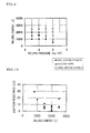
- Fig. 9 is a graph showing a junction state of lead portions of collecting electrodes and an electrode terminal by ultrasonic welding (welding pressure: 2.5 to 4 kg/cm 2 , and welding energy: 500 to 3000 J).
- Fig. 10 is a graph showing a relation between the welding energy [J] and the junction resistance [ ⁇ ] between lead portions of collecting electrodes and an electrode terminal at a welding pressure of 4 kg/cm 2 .
- Fig. 11 is a SEM photography showing a junction interface between lead portions of collecting electrodes and an electrode terminal by ultrasonic welding (welding pressure: 4 kg/cm 2 , welding energy: 2000 J).
- Fig. 12 is a SEM photography showing a junction interface between lead portions of collecting electrodes and an electrode terminal by ultrasonic welding (welding pressure: 4 kg/cm 2 , welding energy: 800 J).
- a manufacturing method of a capacitor according to the present invention aims to make a gross area of protruding portions in an ultrasonic-welding surface be within a range of 5 to 50% of a contact area of the ultrasonic-welding surface and a bundle of lead sections of collecting electrodes at the time of connecting the bundle of lead portions of collecting electrodes to the electrode terminal by ultrasonic welding.
- Figs. 2(a) and 2(b) show an example of the geometry of an ultrasonic-welding surface in a welding head of the present invention
- Fig. 2(a) is a front view
- Fig. 2(b) is a sectional view taken on a line A-A in Fig. 2(a).
- a manufacturing method of a capacitor according to the present invention is mainly characterized in making a gross area of protruding portions 55 in an ultrasonic-welding surface 54 be within a range of 5 to 50% of a contact area of the ultrasonic-welding surface 54 and a bundle of lead sections 4 of collecting electrodes 2, as shown in Fig. 2.
- the area of the protruding portions 55 is 0.005 to 0.050 times as large as the area of the ultrasonic-welding surface 54, and that the protruding portions 55 are uniformly arranged in predetermined intervals in the ultrasonic-welding surface 54.
- each protruding portion 55 is frustoconical as shown in Fig. 2(b) or is cylindrical, and that its end 56 has a shape of a shallow cone.
- a bond resistance in a joint of the collecting electrodes and electrode terminal is at least 30 ⁇ or less.
- the manufacturing method of the capacitor of the present invention can prevent the peeling of lead portions only by ultrasonic welding from the above description. Hence, as shown in Fig. 5, even if a thickness T of the bundle of lead portions 4 exceeds 0.6 mm, or even if the number of sheets of the collecting electrodes exceeds 20 sheets, it is possible to sharply increase the durability of the joint 6 in vibration, cold-heat cycles, and charge and discharge cycles for a long period of time.
- the thickness per sheet of the lead portions used in the present invention is 10 to 100 ⁇ m. It is still more preferable that the thickness is 20 to 50 ⁇ m in consideration of an amount of current flowing to the lead portion, the weight per cell, and dimensions and geometry.
- the collecting electrodes and lead portions that are used in the present invention are made of aluminum to which etching processing is performed.
- the aluminum foil to which etching processing is performed in order to control the thickness of an oxide film uniformly is used is because the electric junction of the collecting electrodes and the polarizable electrode that are made of aluminum foils is stabilized.
- the reason why the lead portions to which etching processing is performed is used is because it is easy to perform formation processing of the lead portions and the collecting electrodes in one piece in a usual manufacturing method.
- the etching processing has the effectiveness of enhancing the stability of the aluminum foil in a capacitor cell.
- the welding head 50 which had the ultrasonic-welding surface 54 shown in Fig. 2 was set in an ultrasonic welder (model 19000 and POWER SUPPLY 900M made by Emerson Japan, Ltd.) shown in Fig. 1.
- dimensions of the ultrasonic-welding surface 54 are a diameter of 4 mm and a height of 1 mm of the protruding portion 55, and the gross area of the protruding portions 55 was 30% of the contact area of the ultrasonic-welding surface 54 and lead portions 4 of the collecting electrode 2.
- the bundle of the above-described lead portions was set in the ultrasonic welder shown in Fig. 1 by overlapping ends of the bundle of the lead portions of the electrode terminal made of aluminum (width: 20 mm, thickness: 2 mm) by 10 mm. Then, the bundle of the lead portions was welded under conditions of welding pressure: 2.5 to 4 kg/cm 2 , and welding energy: 500 to 3000 J, respectively.
- the optimal welding conditions for the junction of the welding head and lead portions of collecting electrodes were a welding pressure of 3 to 4 kg/cm 2 (preferably, 4 kg/cm 2 ) and a welding energy of 1000 to 2500 J.
- the optimal welding energy for the junction of the welding head and the lead portions of collecting electrodes at a welding pressure of 4 kg/cm 2 was 1500 to 2000 J (preferably, 2000 J).
- the manufacturing method of the capacitor according to the present invention not only can certainly perform junction with electrode terminals without increasing any junction resistance only by ultrasonic welding even if the bundle of lead portions of collecting electrodes is thick, or the number of sheets of collecting electrodes is large, but also can contribute to the improvement in the durability in vibration, cold-heat cycles, and charge and discharge cycles over a long period of time.
Landscapes
- Engineering & Computer Science (AREA)
- Power Engineering (AREA)
- Microelectronics & Electronic Packaging (AREA)
- Electric Double-Layer Capacitors Or The Like (AREA)
- Fixed Capacitors And Capacitor Manufacturing Machines (AREA)
Abstract
There is provided a manufacturing method of a capacitor
including: providing the capacitor having positive and
negative polarizable electrodes which generates an electric
double layer; a separator with which the polarizable
electrodes are electrically insulated therebetween; and
collecting electrodes that are made of metal and lead out
charges from the polarizable electrodes, and joining a bundle
of lead portions of the collecting electrodes to an electrode
terminal by ultrasonic welding. A gross area of protruding
portions in an ultrasonic-welding surface is made to be
within a range of 5 to 50% of a contact area of the
ultrasonic-welding surface and lead sections of collecting
electrodes. The manufacturing method can perform
junction of electrode terminals without increasing
junction resistance only by ultrasonic welding even if the
bundle of lead portions of collecting electrodes is thick,
or the number of sheets of collecting electrodes is large.
Description
- The present invention relates to a manufacturing method of a capacitor.
- Now, the application development of capacitors has been actively performed in various kinds of fields because of characteristics of being chargeable and dischargeable in short time.
- In particular, environmental problems and resources problems request the drastic reduction of an amount of fossil fuels used by automobiles. As one of the measures of this reduction, so-called hybrid cars that can reduce the amount of the fossil fuels used by the combined use of fossil fuels and electricity have gotten a lot of attention. In this field, much power densification of high power density type capacitors are requested.
- On the other hand, the use of capacitors as so-called backup power supplies of personal computers or various types of electrical equipment has also increased. Although the high energy density type capacitors are used in this field, much energy densification is requested.
- For this reason, as a capacitor, it is common to use, for example, a
single capacitor cell 12 which has a stacked structure, which is a basic structure of a capacitor as shown in Fig. 7 and is formed by joininglead portions electrodes single electrode cell 10 electrically in parallel, respectively, as shown in Fig. 8. - In addition, as shown in Figure 7, the
single electrode cell 10 has the structure where apolarizable electrode 24 in a positive polarity and apolarizable electrode 26 in a negative polarity are formed on the collectingelectrodes polarizable electrodes polarizable electrodes polarizable electrodes separator 28. - In addition, when the capacitor shown above is actually used, the capacitor is packed in severe packaging suitability (sealing performance, barrier property, antiwear quality, expansion-proof property, etc.) except the electrode terminal in order to prevent leakage, degradation, etc. of the liquid electrolyte.
- Here, for connecting a bundle (for example, one to forty sheets of several tens to hundreds µm thickness of aluminum foils are bundled) of the
lead portions 4 of the collecting electrodes, and the electrode terminal in the capacitor shown above, so as to stably maintain electrical connection over a long period of time, besides ultrasonic welding, a caulking method, a screw cramping method, a pressure joint method, a TIG welding method, etc. have been examined. - In addition, when ultrasonic welding is used, as shown in Fig. 1, by giving ultrasonic vibration from an ultrasonic-
welding surface 52 of awelding head 50 by sandwiching thelead portions 4 of the collectingelectrodes 2 and theelectrode terminal 40 by thewelding head 50 and ananvil 60, applying pressure, and performing welding by using frictional heat by vibration, the bundle oflead portions 4 of the collectingelectrodes 2 and theelectrode terminal 40 are joined as shown in Figs. 4 and 5. - At this time, in ultrasonic welding, usually, although a pattern on an ultrasonic-
welding surface 58 shown in Fig. 3 consisting of two ormore squares 59, that is, a so-called diamond cut pattern is generally used, one or more cracks arise in many cases into one or more corner parts of thesquares 59 which are a welded surface pattern. - In addition, in a capacitor with high energy density, since several tens to hundreds of
single electrode cells 10 in a single capacitor cell are required, the thickness of the bundle oflead portions 4 may exceed 0.6 mm. - For this reason, when junction is performed only by conventional ultrasonic welding (welding using the ultrasonic-
welding surface 58 shown in Fig. 3), as shown in Fig. 6, since sufficient ultrasonic vibration cannot be given to surfaces of the bundle oflead portions 4 to be joined to theelectrode terminal 40, a part of the bundle oflead portions 4 remains as apeeling portion 9 without being welded. Hence, there is a problem that the durability of ajoint 6 in vibration, cold-heat cycles, and charge and discharge cycles over a long period of time drops. - In particular, when a lead portion is made of aluminum to which etching processing is performed, it is easy to peel under the influence of an etching layer on a surface, and hence, ultrasonic welding could not be completed.
- Furthermore, when any one of the caulking method, screw-cramping method, and pressure joint method is used, there is a problem that a junction resistance between lead portions and an electrode terminal increases. If it is tried to obtain a sufficiently low junction resistance when the spot welding method or TIG welding method is used, there is a problem that damage in a lead portion becomes large, and hence, the lead portion is cut.
- Thus, at the time of junction of a lead portion and an electrode terminal, when the thickness of the bundle of the lead portions exceeds 0.6 mm, the number of sheets of collecting electrodes is 20 or more sheets, or the lead portions are made of aluminum to which etching processing is performed, the trouble arises notably.
- The present invention seeks to solve problems of conventional technology and its object is to provide a manufacturing method of a capacitor that can surely perform junction with an electrode terminal only by ultrasonic welding without increasing any junction resistance even if a bundle of lead portions of collecting electrodes becomes thick, or the number of sheets of collecting electrodes is many, and also, can contribute to improvement in the durability in the vibration, a cold-heat cycle, and a charge and discharge cycle over a long period of time.
- That is, according to the present invention, there is provided a manufacturing method of a capacitor, comprising: providing the capacitor comprising positive and negative polarizable electrodes which generate an electric double layer; a separator with which the polarizable electrodes are electrically insulated therebetween; and collecting electrodes that are made of metal and lead out charges from the polarizable electrodes, and joining a bundle of lead portions of the collecting electrodes to an electrode terminal by ultrasonic welding, wherein the total area of protruding portion in an ultrasonic-welding surface is within a range of 5 to 50% of a contact area of the ultrasonic-welding surface and the lead sections of the collecting.
- At this time, it is preferable that the area of the protruding portions is 0.005 to 0.050 times as large as the area of the ultrasonic-welding surface.
- In addition, it is preferable that the protruding portions are uniformly arranged in predetermined intervals on the ultrasonic-welding surface.
- Furthermore, it is preferable that an end of the protruding portion is processed in the shape of a cone having a gradual taper.
- In addition, in the present invention, even if the thickness of the bundle of lead portions exceeds 0.6 mm, or the number of collecting electrodes exceeds 20 sheets, the bundle of lead portions is certainly connectable with an electrode terminal only by ultrasonic welding.
- Moreover, it is preferable that the thickness per sheet of the lead portions is 10 to 100 µm, and in consideration of the amount of current flowing to a lead portion, weight per cell, and dimensions, it is still more preferable that the thickness per sheet of a lead portion is 20 to 50 µm.
- Furthermore, in the present invention, it is preferable that the junction resistance in the joint of collecting electrodes and an electrode terminal is at least 30 µΩ or less, and it is preferable that a collecting electrode and a lead portion are made of aluminum to which etching processing is performed.
- Fig. 1 is an explanatory diagram showing an example of a connection method of lead portions of collecting electrodes and an electrode terminal according to the present invention.
- Figs. 2(a) and 2(b) show an example of a geometry of an ultrasonic-welding surface in a welding head according to the present invention, Fig. 2(a) is a front view, and Fig. 2(b) is a sectional view taken on line A-A in Fig. 2(a).
- Figs. 3(a) and 3(b) show an example of a geometry of an ultrasonic-welding surface in a conventional welding head, Fig. 3(a) is a front view, and Fig. 3(b) is a sectional view taken on a line A-A in Fig. 3(a).
- Fig. 4 is a schematic perspective view showing a junction state of lead portions of collecting electrodes and an electrode terminal in the present invention.
- Fig. 5 is a sectional view taken on a line A-A in Fig. 4.
- Fig. 6 is a schematic sectional view showing a junction state of lead portions of collecting electrodes and an electrode terminal in conventional ultrasonic welding.
- Fig. 7 is a perspective view showing an example of a structure of a single electrode cell.
- Fig. 8 is a perspective view showing an example of a structure of a single capacitor cell.
- Fig. 9 is a graph showing a junction state of lead portions of collecting electrodes and an electrode terminal by ultrasonic welding (welding pressure: 2.5 to 4 kg/cm2, and welding energy: 500 to 3000 J).
- Fig. 10 is a graph showing a relation between the welding energy [J] and the junction resistance [µΩ] between lead portions of collecting electrodes and an electrode terminal at a welding pressure of 4 kg/cm2.
- Fig. 11 is a SEM photography showing a junction interface between lead portions of collecting electrodes and an electrode terminal by ultrasonic welding (welding pressure: 4 kg/cm2, welding energy: 2000 J).
- Fig. 12 is a SEM photography showing a junction interface between lead portions of collecting electrodes and an electrode terminal by ultrasonic welding (welding pressure: 4 kg/cm2, welding energy: 800 J).
- A manufacturing method of a capacitor according to the present invention aims to make a gross area of protruding portions in an ultrasonic-welding surface be within a range of 5 to 50% of a contact area of the ultrasonic-welding surface and a bundle of lead sections of collecting electrodes at the time of connecting the bundle of lead portions of collecting electrodes to the electrode terminal by ultrasonic welding.
- Owing to this, while it is possible to surely perform junction with the electrode terminal without increasing any junction resistance even if the bundle of lead portions of collecting electrodes becomes thick, it is possible to contribute to the improvement in the durability in vibration, cold-heat cycles, and charge and discharge cycles over a long period of time.
- Hereinafter, based on drawings, the present invention will be described further in detail.
- Figs. 2(a) and 2(b) show an example of the geometry of an ultrasonic-welding surface in a welding head of the present invention, Fig. 2(a) is a front view, and Fig. 2(b) is a sectional view taken on a line A-A in Fig. 2(a).
- Here, a manufacturing method of a capacitor according to the present invention is mainly characterized in making a gross area of protruding
portions 55 in an ultrasonic-welding surface 54 be within a range of 5 to 50% of a contact area of the ultrasonic-welding surface 54 and a bundle oflead sections 4 of collectingelectrodes 2, as shown in Fig. 2. - This is because, when the gross area of the protruding
portions 55 in the ultrasonic-welding surface 54 exceeds 50% of the contact area of the ultrasonic-welding surface 54 and thelead portions 4 of collectingelectrodes 2, thewelding head 50 adheres to thelead portions 4 of collectingelectrodes 2, and hence, thelead portions 4 are cut at the time of separating thelead portions 4 from thewelding head 50. - On the other hand, when the gross area of the protruding
portions 55 in the ultrasonic-welding surface 54 is less than 5% of the contact area of the ultrasonic-welding surface 54 and thelead portions 4 of collectingelectrodes 2, junction strength and junction resistance are insufficient. - At this time, it is preferable in the present invention as shown in Fig. 2(a) that the area of the
protruding portions 55 is 0.005 to 0.050 times as large as the area of the ultrasonic-welding surface 54, and that the protrudingportions 55 are uniformly arranged in predetermined intervals in the ultrasonic-welding surface 54. - This is because it is possible not only to avoid a damage of the lead portions due to a crack by suppressing the adhesion of the lead portions and ultrasonic-welding surface at the time of junction, but also to make the bonding strength and junction resistance of the lead portions and electrode terminal good.
- In addition, it is preferable that each
protruding portion 55 is frustoconical as shown in Fig. 2(b) or is cylindrical, and that itsend 56 has a shape of a shallow cone. - Owing to this, since ultrasonic energy can be converged on the protruding
portions 55, it is possible to surely join the lead portions and electrode terminal efficiently. - In addition, it is preferable in the present invention that a bond resistance in a joint of the collecting electrodes and electrode terminal is at least 30 µΩ or less.
- This is because an internal resistance value of a capacitor becomes large if the resistance of the joint becomes high.
- The manufacturing method of the capacitor of the present invention can prevent the peeling of lead portions only by ultrasonic welding from the above description. Hence, as shown in Fig. 5, even if a thickness T of the bundle of
lead portions 4 exceeds 0.6 mm, or even if the number of sheets of the collecting electrodes exceeds 20 sheets, it is possible to sharply increase the durability of thejoint 6 in vibration, cold-heat cycles, and charge and discharge cycles for a long period of time. - In addition, it is preferable that the thickness per sheet of the lead portions used in the present invention is 10 to 100 µm. It is still more preferable that the thickness is 20 to 50 µm in consideration of an amount of current flowing to the lead portion, the weight per cell, and dimensions and geometry.
- Furthermore, it is preferable that the collecting electrodes and lead portions that are used in the present invention are made of aluminum to which etching processing is performed.
- Usually, on the surface of an aluminum foil, a natural oxidation film is generated easily and the thickness of the oxide film is not uniform. The reason why the aluminum foil to which etching processing is performed in order to control the thickness of an oxide film uniformly is used is because the electric junction of the collecting electrodes and the polarizable electrode that are made of aluminum foils is stabilized. The reason why the lead portions to which etching processing is performed is used is because it is easy to perform formation processing of the lead portions and the collecting electrodes in one piece in a usual manufacturing method. In addition, the etching processing has the effectiveness of enhancing the stability of the aluminum foil in a capacitor cell.
- Hereafter, although the present invention will be described further in detail on the basis of embodiments, the present invention is not restricted to these embodiments.
- The
welding head 50 which had the ultrasonic-weldingsurface 54 shown in Fig. 2 was set in an ultrasonic welder (model 19000 and POWER SUPPLY 900M made by Emerson Japan, Ltd.) shown in Fig. 1. - In addition, dimensions of the ultrasonic-welding
surface 54 are a diameter of 4 mm and a height of 1 mm of the protrudingportion 55, and the gross area of the protrudingportions 55 was 30% of the contact area of the ultrasonic-weldingsurface 54 andlead portions 4 of the collectingelectrode 2. - Next, twenty eight sheets of lead portions (width: 20 mm, length: 30 mm) of the 50-µm thick collecting electrodes consisting of aluminum foils to which the etching processing was performed are stacked, and a bundle of lead portions was produced respectively.
- The bundle of the above-described lead portions was set in the ultrasonic welder shown in Fig. 1 by overlapping ends of the bundle of the lead portions of the electrode terminal made of aluminum (width: 20 mm, thickness: 2 mm) by 10 mm. Then, the bundle of the lead portions was welded under conditions of welding pressure: 2.5 to 4 kg/cm2, and welding energy: 500 to 3000 J, respectively.
- At this time, each junction state of the lead portions of the collecting electrodes and electrode terminal was observed. The result is shown in Fig. 9.
- In addition, a relation between the welding energy [J] and the junction resistance [µΩ] between the lead portions of the collecting electrodes and the electrode terminal at the welding pressure of 4 kg/cm2 is shown in Fig. 10.
- Furthermore, when welding pressure was 4 kg/cm2 and welding energy was 800 J (refer to Fig. 12) and 2000 J (refer to Fig. 11), a junction interface between the lead portions of collecting electrodes and electrode terminal was observed with a scanning electron micro scope (SEM).
- From the result of Fig. 9, it was confirmed that the optimal welding conditions for the junction of the welding head and lead portions of collecting electrodes were a welding pressure of 3 to 4 kg/cm2 (preferably, 4 kg/cm2) and a welding energy of 1000 to 2500 J.
- In addition, from the result of Figs. 10 to 12, it was confirmed that the optimal welding energy for the junction of the welding head and the lead portions of collecting electrodes at a welding pressure of 4 kg/cm2 was 1500 to 2000 J (preferably, 2000 J).
- As described above, the manufacturing method of the capacitor according to the present invention not only can certainly perform junction with electrode terminals without increasing any junction resistance only by ultrasonic welding even if the bundle of lead portions of collecting electrodes is thick, or the number of sheets of collecting electrodes is large, but also can contribute to the improvement in the durability in vibration, cold-heat cycles, and charge and discharge cycles over a long period of time.
Claims (9)
- A manufacturing method of a capacitor, comprising:providing the capacitor comprising positive and negative polarizable electrodes which generate an electric double layer; a separator with which the polarizable electrodes are electrically insulated therebetween; and collecting electrodes that are made of metal and lead out charges from the polarizable electrodes, andjoining a bundle of lead portions of the collecting electrodes to an electrode terminal by ultrasonic welding,wherein the gross area of protruding portions in an ultrasonic-welding surface is within a range of 5 to 50% of a contact area of the ultrasonic-welding surface and the lead sections of the collecting electrodes.
- The manufacturing method of a capacitor according to claim 1, wherein said area of protruding portions is 0.005 to 0.050 times as large as an area of the ultrasonic-welding surface.
- The manufacturing method of a capacitor according to any one of claims 1 and 2, wherein the protruding portions are uniformly arranged in predetermined intervals in the ultrasonic-welding surface.
- The manufacturing method of a capacitor according to any one of claims 1 to 3, wherein an end of the protruding portion is processed in a shape of a cone having a gradual taper.
- The manufacturing method of a capacitor according to any one of claims 1 to 4, wherein thickness of the bundle of lead portions exceeds 0.6 mm.
- The manufacturing method of a capacitor according to any one of claims 1 to 5, wherein the number of sheets of the bundle of lead portions exceeds 20 sheets.
- The manufacturing method of a capacitor according to any one of claims 1 to 6, wherein thickness per sheet of the lead portions is 10 to 100 µm.
- The manufacturing method of a capacitor according to any one of claims 1 to 7, wherein bond resistance in a connection of the collecting electrodes and the electrode terminal is at least 30 µΩ or less.
- The manufacturing method of a capacitor according to any one of claims 1 to 8, wherein the collecting electrode and the lead portion are made of aluminum to which etching processing is given.
Applications Claiming Priority (2)
| Application Number | Priority Date | Filing Date | Title |
|---|---|---|---|
| JP2000397320 | 2000-12-27 | ||
| JP2000397320A JP2002198262A (en) | 2000-12-27 | 2000-12-27 | Method for manufacturing capacitor |
Publications (1)
| Publication Number | Publication Date |
|---|---|
| EP1221704A2 true EP1221704A2 (en) | 2002-07-10 |
Family
ID=18862456
Family Applications (1)
| Application Number | Title | Priority Date | Filing Date |
|---|---|---|---|
| EP01310912A Withdrawn EP1221704A2 (en) | 2000-12-27 | 2001-12-27 | Manufacturing method of capacitor |
Country Status (3)
| Country | Link |
|---|---|
| US (1) | US20020112330A1 (en) |
| EP (1) | EP1221704A2 (en) |
| JP (1) | JP2002198262A (en) |
Families Citing this family (4)
| Publication number | Priority date | Publication date | Assignee | Title |
|---|---|---|---|---|
| JP5472687B2 (en) * | 2009-06-04 | 2014-04-16 | トヨタ自動車株式会社 | Secondary battery and manufacturing method thereof |
| JP5265586B2 (en) * | 2010-01-15 | 2013-08-14 | 太陽誘電株式会社 | Electrochemical devices |
| CN104396050B (en) | 2012-06-28 | 2016-08-17 | 丰田自动车株式会社 | The manufacture method of battery and battery |
| KR102323041B1 (en) | 2019-02-01 | 2021-11-08 | 주식회사 엘지에너지솔루션 | Electrode Assembly Comprising Different Pressure Welded Part on Weld Surface of Electrode Tab and Ultrasonic Welding Device for Manufacturing the Same |
Family Cites Families (5)
| Publication number | Priority date | Publication date | Assignee | Title |
|---|---|---|---|---|
| US3754310A (en) * | 1971-07-29 | 1973-08-28 | Underwriters Safety Device Co | Method of making an electrical assembly fastened with thermoplastic eyelet |
| US4647325A (en) * | 1984-07-12 | 1987-03-03 | Presto Products, Incorporated | Ultrasonic spot welding tip assembly and method for using the same |
| AU675937B2 (en) * | 1992-04-10 | 1997-02-27 | W.L. Gore & Associates, Inc. | A method of ultrasonically welding articles of porous polytetrafluoroethylene |
| US5862035A (en) * | 1994-10-07 | 1999-01-19 | Maxwell Energy Products, Inc. | Multi-electrode double layer capacitor having single electrolyte seal and aluminum-impregnated carbon cloth electrodes |
| US5922215A (en) * | 1996-10-15 | 1999-07-13 | Pacesetter, Inc. | Method for making anode foil for layered electrolytic capacitor and capacitor made therewith |
-
2000
- 2000-12-27 JP JP2000397320A patent/JP2002198262A/en not_active Withdrawn
-
2001
- 2001-12-21 US US10/036,754 patent/US20020112330A1/en not_active Abandoned
- 2001-12-27 EP EP01310912A patent/EP1221704A2/en not_active Withdrawn
Also Published As
| Publication number | Publication date |
|---|---|
| JP2002198262A (en) | 2002-07-12 |
| US20020112330A1 (en) | 2002-08-22 |
Similar Documents
| Publication | Publication Date | Title |
|---|---|---|
| US7718312B2 (en) | Battery | |
| KR100878700B1 (en) | Electrode plate for battery cell production and its manufacturing method | |
| JP4588331B2 (en) | Square battery and manufacturing method thereof | |
| JP5656592B2 (en) | Secondary battery | |
| US8142922B2 (en) | Secondary battery and method for manufacturing secondary battery | |
| KR20180061681A (en) | Battery Cell Having Double Welding Structure | |
| US20220352606A1 (en) | Secondary battery and method for manufacturing same | |
| CN107658413A (en) | Layer-built battery and its manufacture method | |
| JP2017216148A (en) | Power storage device, power storage device, and method for manufacturing power storage device | |
| KR20090132494A (en) | Electrode tab and lithium secondary battery comprising same | |
| JP2000260417A (en) | Stacked battery | |
| JPH11339758A (en) | Electrode-wound battery | |
| JP3733403B2 (en) | Electrode wound type battery | |
| WO2022059796A1 (en) | Electricity storage device, and method for manufacturing same | |
| JP4843893B2 (en) | battery | |
| JP5574542B2 (en) | Method for joining a plurality of electrode plate components | |
| JP2000235853A (en) | Power generation element | |
| JP2001093506A (en) | Electrode joining method for storage element | |
| JP2022097943A (en) | Battery and manufacturing method thereof | |
| US20020112330A1 (en) | Manufacturing method of capacitor | |
| JP2000231913A (en) | Cylindrical battery | |
| JP2011113811A (en) | Battery and method of manufacturing the same | |
| JP3652550B2 (en) | Lithium secondary battery and manufacturing method thereof | |
| JP7079694B2 (en) | Power storage module | |
| JP2003249269A (en) | Non-aqueous electrolyte secondary battery |
Legal Events
| Date | Code | Title | Description |
|---|---|---|---|
| PUAI | Public reference made under article 153(3) epc to a published international application that has entered the european phase |
Free format text: ORIGINAL CODE: 0009012 |
|
| AK | Designated contracting states |
Kind code of ref document: A2 Designated state(s): AT BE CH CY DE DK ES FI FR GB GR IE IT LI LU MC NL PT SE TR |
|
| AX | Request for extension of the european patent |
Free format text: AL;LT;LV;MK;RO;SI |
|
| STAA | Information on the status of an ep patent application or granted ep patent |
Free format text: STATUS: THE APPLICATION HAS BEEN WITHDRAWN |
|
| 18W | Application withdrawn |
Effective date: 20030620 |