EP1220444A1 - Differential output amplifier arrangement - Google Patents
Differential output amplifier arrangement Download PDFInfo
- Publication number
- EP1220444A1 EP1220444A1 EP00403709A EP00403709A EP1220444A1 EP 1220444 A1 EP1220444 A1 EP 1220444A1 EP 00403709 A EP00403709 A EP 00403709A EP 00403709 A EP00403709 A EP 00403709A EP 1220444 A1 EP1220444 A1 EP 1220444A1
- Authority
- EP
- European Patent Office
- Prior art keywords
- arrangement
- amplifier
- resistor
- input terminal
- doa
- Prior art date
- Legal status (The legal status is an assumption and is not a legal conclusion. Google has not performed a legal analysis and makes no representation as to the accuracy of the status listed.)
- Withdrawn
Links
- 230000008878 coupling Effects 0.000 claims description 6
- 238000010168 coupling process Methods 0.000 claims description 6
- 238000005859 coupling reaction Methods 0.000 claims description 6
- 101100396986 Saccharomyces cerevisiae (strain ATCC 204508 / S288c) INN1 gene Proteins 0.000 abstract description 6
- 101150071403 INP1 gene Proteins 0.000 abstract description 2
- 101150016601 INP2 gene Proteins 0.000 abstract description 2
- 230000005540 biological transmission Effects 0.000 description 3
- 238000006880 cross-coupling reaction Methods 0.000 description 3
- 101000730648 Homo sapiens Phospholipase A-2-activating protein Proteins 0.000 description 1
- 102100032572 Phospholipase A-2-activating protein Human genes 0.000 description 1
- 230000000694 effects Effects 0.000 description 1
- 238000000034 method Methods 0.000 description 1
Images
Classifications
-
- H—ELECTRICITY
- H03—ELECTRONIC CIRCUITRY
- H03F—AMPLIFIERS
- H03F3/00—Amplifiers with only discharge tubes or only semiconductor devices as amplifying elements
- H03F3/34—DC amplifiers in which all stages are DC-coupled
- H03F3/343—DC amplifiers in which all stages are DC-coupled with semiconductor devices only
- H03F3/347—DC amplifiers in which all stages are DC-coupled with semiconductor devices only in integrated circuits
Definitions
- the present invention relates to a differential output amplifier arrangement as defined in the non-characteristic part of claim 1.
- differential output amplifier arrangement is already known in the art, e.g. from the European Patent Application EP 0 901 221 from applicant Alcatel, entitled 'Differential Output Amplifier Arrangement and Method for Tuning the Output Impedance of a Differential Output Amplifier'.
- the differential output amplifier arrangement disclosed therein is active back terminated.
- the signal source is coupled to the positive input terminals of the operational amplifiers, whereas a resistor interconnects the negative input terminals of the operational amplifiers. This configuration at the entrance does not allow to realise the biasing and gain control for the amplifier arrangement with a minimum amount of components.
- An object of the present invention is to provide a differential output amplifier arrangement similar to the known one, but whose biasing and gain control can be realised with a minimum amount of components.
- a signal source can be directly coupled to the input terminals of the amplifier arrangement according to the present invention.
- This signal source could not be directly coupled to the input terminals of the prior art amplifier arrangement because the biasing there required two resistors to be inserted between the signal source and the input terminals of the amplifier arrangement.
- These biasing resistors inherently form part of the amplifier arrangement according to the present invention wherein no longer a resistor interconnecting the negative input terminals of the two operational amplifiers is needed, which was the case in the prior art solution.
- the term 'coupled' should not be interpreted as being limitative to direct connections only.
- the scope of the expression 'a device A coupled to a device B' should not be limited to devices or systems wherein an output of device A is directly connected to an input of device B. It means that there exists a path between an output of A and an input of B which may be a path including other devices or means.
- the biasing resistors preferably have substantial equal resistance values.
- the amplifier arrangement according to the present invention becomes a stable system from point of view of system theory, which implies that the arrangement will not oscillate.
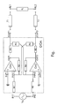
- the differential output amplifier arrangement DOA represented in the drawing has two arrangement input terminals denoted by IN1 and IN2, and two arrangement output terminals denoted by ZOUT1 and ZOUT2. To the arrangement input terminals IN1 and IN2 terminals of a differential input signal source are coupled. The arrangement output terminals ZOUT1 and ZOUT2 are coupled to transmission lines T1 and T2.
- the differential output amplifier arrangement DOA further includes two operational amplifiers, OA1 and OA2, having respective non-inverting input terminals INP1 and INP2, respective inverting input terminals INN1 and INN2, and having respective output terminals OUT1 and OUT2.
- the output terminal OUT1 of the first operational amplifier OA1 is coupled to the first arrangement output terminal ZOUT1 via a first resistor R1, and feedback coupled to the inverting input terminal INN1 of this first operational amplifier OA1 via a second resistor R2.
- the output terminal OUT2 of the second operational amplifier OA2 is coupled to the second arrangement output terminal ZOUT2 via a third resistor R3, and feedback coupled to the inverting input terminal INN2 of this second operational amplifier OA2 via a fourth resistor R4.
- the differential output amplifier arrangement DOA1 contains two additional resistors, a fifth resistor R5 cross-coupling the first arrangement output terminal ZOUT1 to the inverting input terminal INN2 of the second operational amplifier OA2, and a sixth resistor R6 cross-coupling the second arrangement output terminal ZOUT2 to the inverting input terminal INN1 of the first operational amplifier OA1.
- These two resistors, R5 and R6, together with the first resistor R1 and the third resistor R3 constitute an active back termination that allows to tune the output impedance of the arrangement DOA to a desired value.
- the output impedance of the arrangement DOA matches a load impedance which is denoted by RL in the drawing, and which in the drawing is coupled to the transmission lines T1 and T2 via terminals RL1 and RL2.
- the characteristic impedance of the transmission lines T1 and T2 is supposed to be equal to RL/2 for matching purposes.
- the voltage drop over the first resistor R1 and third resistor R3 of this active back termination allow the arrangement DOA to deliver an output signal having a given power with reduced supply voltage for the operational amplifiers OA1 and OA2, and/or with an increased dynamic range for both operational amplifiers OA1 and OA2.
- the differential output amplifier arrangement DOA furthermore contains a seventh resistor R7 coupled between the first arrangement input terminal IN1 and the inverting input terminal INN1 of the first operational amplifier OA1, and an eighth resistor R8, coupled between the second arrangement input terminal IN2 and the inverting input terminal INN2 of the second operational amplifier OA2. Between the first input terminal IN1 and the second input terminal IN2 of the arrangement DOA, the differential input signal Vs is applied.
- A R7.R2 - R7.R1 + R7.R5 + 2.R2.R5 2.R7.R1.R5 + RL.R7.R5 + RL.R7.R1- RL.R7.R2 .RL
- the resistance values R1, R2, R5 and R7 on the basis of the formula's (1) and (2) can be chosen so that the desired gain and arrangement output impedance are realised.
- the resistors R7 and R8 that allow to tune the gain A of the differential output amplifier arrangement DOA realise the input DC biasing.
- Such biasing is not realised by the arrangement known from EP 0 901 221, and has to be provided for there by two additional resistors coupling the input terminals of the operational amplifiers to the ground or a reference level.
- the biasing and gain control is thus more efficiently realised in the arrangement according to the present invention, since less components are required in the end.
- An embodiment of the amplifier arrangement DOA can be used for instance in an ADSL (Asynchronous Digital Subscriber Line) line driver.
- the characteristic impedance in such a line driver is transformed by a hybrid into a value of 12.5 Ohm observed at the output of the operational amplifiers OA1 and OA2.
- the load resistance RL has an equivalent resistance value of 25 Ohm for matching purposes.
- the desired gain A is set by surrounding system considerations, that fall beyond the scope of this patent application.
- the operational amplifiers and resistance values may be chosen as follows:
Landscapes
- Engineering & Computer Science (AREA)
- Microelectronics & Electronic Packaging (AREA)
- Power Engineering (AREA)
- Amplifiers (AREA)
Abstract
A differential output amplifier arrangement (DOA) comprises two operational amplifier (OA1, OA2) each having a feedback resistor (R2, R4). A pair of output resistors (R1, R3) couples the output terminals (OUT1, OUT2) of the operational amplifiers (OA1, OA2) to respective output terminals (ZOUTI, ZOUT2) of the arrangement (DOA), and a pair of input terminals (R7, R8) couples input terminals (IN1, IN2) of the arrangement (DOA) to negative polarity type input terminals (INN1, INN2) of the respective operational amplifiers (OA1, OA2). The positive polarity type input terminals (INP1, INP2) of the operational amplifiers (OA1, OA2) are grounded. Two additional resistors (R5, R6) cross-couple the output terminals (ZOUT1, ZOUT2) of the arrangement (DOA) to the negative polarity type input terminals (INN2, INN1) of the cross-coupled operational amplifiers (OA2, OA1). <IMAGE>
Description
The present invention relates to a differential output amplifier
arrangement as defined in the non-characteristic part of claim 1.
Such a differential output amplifier arrangement is already known in the
art, e.g. from the European Patent Application EP 0 901 221 from applicant
Alcatel, entitled 'Differential Output Amplifier Arrangement and Method for
Tuning the Output Impedance of a Differential Output Amplifier'. The differential
output amplifier arrangement disclosed therein is active back terminated. This
means that a pair of resistors - R3 and R30 in the drawing of EP 0 901 221 - is
foreseen between the outputs of the operational amplifiers and the output
terminals of the arrangement, and that a pair of resistors - R4 and R40 in the
drawing of EP 0 901 221 - is foreseen cross-coupling the output terminals of the
arrangement to the negative input terminals of the cross-coupled operational
amplifiers. Thanks to this active back termination, the power consumed by the
differential output amplifier arrangement to generate a signal with a given level,
reduces drastically, e.g. by a factor 2. The signal source is coupled to the positive
input terminals of the operational amplifiers, whereas a resistor interconnects the
negative input terminals of the operational amplifiers. This configuration at the
entrance does not allow to realise the biasing and gain control for the amplifier
arrangement with a minimum amount of components.
An object of the present invention is to provide a differential output
amplifier arrangement similar to the known one, but whose biasing and gain
control can be realised with a minimum amount of components.
According to the invention, this object is achieved by the differential output
amplifier arrangement defined in claim 1.
Indeed, thanks to the presence of the seventh and eight resistors, which
provide biasing and gain control, a signal source can be directly coupled to the
input terminals of the amplifier arrangement according to the present invention.
This signal source could not be directly coupled to the input terminals of the prior
art amplifier arrangement because the biasing there required two resistors to be
inserted between the signal source and the input terminals of the amplifier
arrangement. These biasing resistors inherently form part of the amplifier
arrangement according to the present invention wherein no longer a resistor
interconnecting the negative input terminals of the two operational amplifiers is
needed, which was the case in the prior art solution.
It is to be noticed that the term 'comprising', used in the claims, should
not be interpreted as being limitative to the means listed thereafter. Thus, the
scope of the expression 'a device comprising means A and B' should not be
limited to devices consisting only of components A and B. It means that with
respect to the present invention, the only relevant components of the device are A
and B.
Similarly, it is to be noticed that the term 'coupled', also used in the
claims, should not be interpreted as being limitative to direct connections only.
Thus, the scope of the expression 'a device A coupled to a device B' should not
be limited to devices or systems wherein an output of device A is directly
connected to an input of device B. It means that there exists a path between an
output of A and an input of B which may be a path including other devices or
means.
An additional feature of the differential output amplifier arrangement
according to the present invention is defined in claim 2.
Thus, a better load balance of the two operational amplifiers is obtained if
the feedback resistors have substantially identical resistance values.
Additional advantageous features of the differential output amplifier
arrangement according to the present invention are defined in claims 3 and 4.
In this way, by having the resistors of the active back termination pair-wise
substantially equal, not only a better load balance of the operational amplifiers is
obtained but also the design criteria and formulas that allow to select the values
of the back termination resistors so that specific characteristics are obtained,
become much simpler. This is explained in the already cited European Patent
Application EP 0 901 221.
Another advantageous feature of the differential output amplifier
arrangement according to the present invention is defined in claim 5.
Thus, the biasing resistors preferably have substantial equal resistance
values.
Still an advantageous feature of the differential output amplifier
arrangement according to the present invention is defined in claim 6.
In this way, the amplifier arrangement according to the present invention
becomes a stable system from point of view of system theory, which implies that
the arrangement will not oscillate.
The above mentioned and other objects and features of the invention will
become more apparent and the invention itself will be best understood by
referring to the following description of an embodiment taken in conjunction with
the accompanying drawing that represents an embodiment of the differential
output amplifier arrangement according to the present invention.
The differential output amplifier arrangement DOA represented in the
drawing has two arrangement input terminals denoted by IN1 and IN2, and two
arrangement output terminals denoted by ZOUT1 and ZOUT2. To the
arrangement input terminals IN1 and IN2 terminals of a differential input signal
source are coupled. The arrangement output terminals ZOUT1 and ZOUT2 are
coupled to transmission lines T1 and T2.
The differential output amplifier arrangement DOA further includes two
operational amplifiers, OA1 and OA2, having respective non-inverting input
terminals INP1 and INP2, respective inverting input terminals INN1 and INN2,
and having respective output terminals OUT1 and OUT2. The output terminal
OUT1 of the first operational amplifier OA1 is coupled to the first arrangement
output terminal ZOUT1 via a first resistor R1, and feedback coupled to the
inverting input terminal INN1 of this first operational amplifier OA1 via a second
resistor R2. Similarly, the output terminal OUT2 of the second operational
amplifier OA2 is coupled to the second arrangement output terminal ZOUT2 via
a third resistor R3, and feedback coupled to the inverting input terminal INN2 of
this second operational amplifier OA2 via a fourth resistor R4.
The differential output amplifier arrangement DOA1 contains two
additional resistors, a fifth resistor R5 cross-coupling the first arrangement output
terminal ZOUT1 to the inverting input terminal INN2 of the second operational
amplifier OA2, and a sixth resistor R6 cross-coupling the second arrangement
output terminal ZOUT2 to the inverting input terminal INN1 of the first
operational amplifier OA1. These two resistors, R5 and R6, together with the first
resistor R1 and the third resistor R3 constitute an active back termination that
allows to tune the output impedance of the arrangement DOA to a desired value.
Typically it is desired that the output impedance of the arrangement DOA
matches a load impedance which is denoted by RL in the drawing, and which in
the drawing is coupled to the transmission lines T1 and T2 via terminals RL1 and
RL2. The characteristic impedance of the transmission lines T1 and T2 is
supposed to be equal to RL/2 for matching purposes. As is explained in the
already cited European Patent Application EP 0 901 221, the voltage drop over
the first resistor R1 and third resistor R3 of this active back termination allow the
arrangement DOA to deliver an output signal having a given power with reduced
supply voltage for the operational amplifiers OA1 and OA2, and/or with an
increased dynamic range for both operational amplifiers OA1 and OA2.
The differential output amplifier arrangement DOA furthermore contains a
seventh resistor R7 coupled between the first arrangement input terminal IN1 and
the inverting input terminal INN1 of the first operational amplifier OA1, and an
eighth resistor R8, coupled between the second arrangement input terminal IN2
and the inverting input terminal INN2 of the second operational amplifier OA2.
Between the first input terminal IN1 and the second input terminal IN2 of the
arrangement DOA, the differential input signal Vs is applied.
The formula for the output impedance of the differential output amplifier
arrangement DOA, assuming that the resistors R1 and R3, R2 and R4, R5 and
R6, R7 and R8 pair-wise have substantially identical resistance values, is given
by:
ZOUT = 2.R1.R5 R1 + R5 - R2
From this formula, it is understood that the sum of the resistance values R1
and R5 has to exceed the resistance value R2, a requirement that is also obtained
from stability analysis for the arrangement DOA.
The gain of the differential output amplifier arrangement DOA, again
assuming that the resistors R1 and R3, R2 and R4, R5 and R6, R7 and R8 pair-wise
have substantially identical resistance values, is given by:
A = R7.R2 - R7.R1 + R7.R5 + 2.R2.R52.R7.R1.R5 + RL.R7.R5 + RL.R7.R1- RL.R7.R2 .RL
The resistance values R1, R2, R5 and R7 on the basis of the formula's (1)
and (2) can be chosen so that the desired gain and arrangement output
impedance are realised. Moreover, the resistors R7 and R8 that allow to tune the
gain A of the differential output amplifier arrangement DOA, realise the input
DC biasing. Such biasing is not realised by the arrangement known from EP 0
901 221, and has to be provided for there by two additional resistors coupling
the input terminals of the operational amplifiers to the ground or a reference
level. The biasing and gain control is thus more efficiently realised in the
arrangement according to the present invention, since less components are
required in the end.
Both formula's (1) and (2) assume that the operational amplifiers OA1
and OA2 are 'ideal' operational amplifiers, i.e. having an infinite input
impedance, an infinite open loop gain, and a zero output impedance. Some
precautions have to be taken when selecting the values for the resistors taking
into account that in reality 'ideal' operational amplifiers do not exist.
An embodiment of the amplifier arrangement DOA can be used for
instance in an ADSL (Asynchronous Digital Subscriber Line) line driver. The
characteristic impedance in such a line driver is transformed by a hybrid into a
value of 12.5 Ohm observed at the output of the operational amplifiers OA1 and
OA2. The load resistance RL has an equivalent resistance value of 25 Ohm for
matching purposes. The desired gain A is set by surrounding system
considerations, that fall beyond the scope of this patent application. For such an
embodiment, the operational amplifiers and resistance values may be chosen as
follows:
- For the operational amplifiers, current amplifiers such as the AD816 may be chosen, because of their excellent current drive capability, and their low high frequency distortion, important characteristics for the ADSL application, as will be recognised by persons skilled in the art.
- The feedback resistors R2 and R4 are selected to obtain the desired gain-bandwidth product for the amplifier. These values are provided by the data sheets from the manufacturers of the operational amplifiers.
- R1 and R3 should on the one hand should be as small as possible to allow maximum power to the load. Since the operational amplifiers OA1 and OA2 are not ideal and in a closed-loop configuration by the presence of the feedback resistors R2 and R4, the non-zero output impedance of these amplifiers adds to the value of the resistors R1 and R3. To minimise this effect, the resistance values for R1 and R3 are selected to be at least one order of magnitude larger than the amplifier output impedance value.
- From the formula's (1) and (2), the values of R5 and R7 are then calculated.
While the principles of the invention have been described above in
connection with specific apparatus, it is to be clearly understood that this
description is made only by way of example and not as a limitation on the scope
of the invention.
Claims (6)
- Differential output amplifier arrangement (DOA) comprising:CHARACTERISED IN THAT said first amplifier input terminal (INP1 ) of said first operational amplifier (OA1) is coupled to a ground and said first amplifier input terminal (INP2) of said second operational amplifier is coupled to said ground, and in that said differential output amplifier arrangement (DOA) further comprises:a first arrangement input terminal (IN1) and a second arrangement input terminal (IN2) for respectively coupling to a first terminal and a second terminal of an input signal source (Vs);a first arrangement output terminal (ZOUT1) and a second arrangement output terminal (ZOUT2) for delivering a differential output voltage, said differential output;a first operational amplifier (OA1) having a first amplifier input terminal (INP1) of a first polarity type (+), and a second amplifier input terminal (INN1) of a second polarity type (-) opposite of said first polarity type (+), and an amplifier output terminal (OUT1) coupled to said first arrangement output terminal (ZOUT1) via a first resistor (R1) and coupled to said second amplifier input terminal (INN1) of said first operational amplifier (OA1) via a second resistor (R2);a second operational amplifier (OA2), having a first input terminal (INP2) of said first polarity type (+), and a second amplifier input terminal (INN2) of said second polarity type (-), and an amplifier output terminal (OUT2) coupled to said second arrangement output terminal (ZOUT2) via third resistor (R3) and coupled to said second amplifier input terminal (INN2) of said second operational amplifier (OA2) via a fourth resistor (R4);a fifth resistor (R5) coupling said first arrangement output terminal (ZOUT1) to said second amplifier input terminal (INN2) of said second operational amplifier (OA2), and a sixth resistor (R6) coupling said second arrangement output terminal (ZOUT2) to said second amplifier input terminal (INN1) of said first operational amplifier (OA1),a seventh resistor (R7) coupling said first arrangement input terminal (IN1) to said second amplifier input terminal (INN1) of said first operational amplifier (OA1), and an eight resistor (R8) coupling said second arrangement input terminal (IN2) to said second amplifier input terminal (INN2) of said second operational amplifier (OA2).
- Differential output amplifier arrangement (DOA) according to claim 1,
CHARACTERISED IN THAT said second resistor (R2) and said fourth resistor (R4) have substantially identical resistance values. - Differential output amplifier arrangement (DOA) according to claim 1,
CHARACTERISED IN THAT said first resistor (R1) and said third resistor (R3) have substantially identical resistance values. - Differential output amplifier arrangement (DOA) according to claim 1,
CHARACTERISED IN THAT said fifth resistor (R5) and said sixth resistor (R6) have substantially identical resistance values. - Differential output amplifier arrangement (DOA) according to claim 1,
CHARACTERISED IN THAT said seventh resistor (R7) and said eighth resistor (R8) have substantially identical resistance values. - Differential output amplifier arrangement (DOA) according to any one of the previous claims,
CHARACTERISED IN THAT the resistance value of said second resistor (R2) is smaller than the sum of the resistance values of said first resistor (R1) and said fifth resistor (R5).
Priority Applications (3)
| Application Number | Priority Date | Filing Date | Title |
|---|---|---|---|
| EP00403709A EP1220444A1 (en) | 2000-12-28 | 2000-12-28 | Differential output amplifier arrangement |
| JP2001388784A JP2002223134A (en) | 2000-12-28 | 2001-12-21 | Differential output amplifier device |
| US10/026,434 US20020118063A1 (en) | 2000-12-28 | 2001-12-27 | Differential output amplifier arrangement |
Applications Claiming Priority (1)
| Application Number | Priority Date | Filing Date | Title |
|---|---|---|---|
| EP00403709A EP1220444A1 (en) | 2000-12-28 | 2000-12-28 | Differential output amplifier arrangement |
Publications (1)
| Publication Number | Publication Date |
|---|---|
| EP1220444A1 true EP1220444A1 (en) | 2002-07-03 |
Family
ID=8174016
Family Applications (1)
| Application Number | Title | Priority Date | Filing Date |
|---|---|---|---|
| EP00403709A Withdrawn EP1220444A1 (en) | 2000-12-28 | 2000-12-28 | Differential output amplifier arrangement |
Country Status (3)
| Country | Link |
|---|---|
| US (1) | US20020118063A1 (en) |
| EP (1) | EP1220444A1 (en) |
| JP (1) | JP2002223134A (en) |
Cited By (1)
| Publication number | Priority date | Publication date | Assignee | Title |
|---|---|---|---|---|
| US7330703B2 (en) | 2003-06-26 | 2008-02-12 | Broadcom Corporation | Transceiver for bidirectional frequency division multiplexed transmission |
Families Citing this family (2)
| Publication number | Priority date | Publication date | Assignee | Title |
|---|---|---|---|---|
| TWI346446B (en) * | 2008-04-21 | 2011-08-01 | Advanced Analog Technology Inc | Multi-input operational amplifier and method for reducing input offset thereof |
| WO2012032736A1 (en) * | 2010-09-10 | 2012-03-15 | 旭化成エレクトロニクス株式会社 | Amplification circuit |
Citations (3)
| Publication number | Priority date | Publication date | Assignee | Title |
|---|---|---|---|---|
| EP0809353A2 (en) * | 1996-05-20 | 1997-11-26 | Kabushiki Kaisha Toshiba | Amplifier for cancelling noise between circuit systems |
| EP0901221A1 (en) * | 1997-09-05 | 1999-03-10 | Alcatel | Differential output amplifier arrangement and method for tuning the output impedance of a differential output amplifier |
| FR2778513A1 (en) * | 1998-05-06 | 1999-11-12 | Matra Nortel Communications | Analogue signal processing circuit for symmetrical signal components |
-
2000
- 2000-12-28 EP EP00403709A patent/EP1220444A1/en not_active Withdrawn
-
2001
- 2001-12-21 JP JP2001388784A patent/JP2002223134A/en not_active Withdrawn
- 2001-12-27 US US10/026,434 patent/US20020118063A1/en not_active Abandoned
Patent Citations (3)
| Publication number | Priority date | Publication date | Assignee | Title |
|---|---|---|---|---|
| EP0809353A2 (en) * | 1996-05-20 | 1997-11-26 | Kabushiki Kaisha Toshiba | Amplifier for cancelling noise between circuit systems |
| EP0901221A1 (en) * | 1997-09-05 | 1999-03-10 | Alcatel | Differential output amplifier arrangement and method for tuning the output impedance of a differential output amplifier |
| FR2778513A1 (en) * | 1998-05-06 | 1999-11-12 | Matra Nortel Communications | Analogue signal processing circuit for symmetrical signal components |
Cited By (3)
| Publication number | Priority date | Publication date | Assignee | Title |
|---|---|---|---|---|
| US7330703B2 (en) | 2003-06-26 | 2008-02-12 | Broadcom Corporation | Transceiver for bidirectional frequency division multiplexed transmission |
| US7450715B2 (en) | 2003-06-26 | 2008-11-11 | Broadcom Corporation | Transceiver for bidirectional frequency division multiplexed transmission |
| US7940707B2 (en) | 2003-06-26 | 2011-05-10 | Broadcom Corporation | Transceiver for bidirectional frequency division multiplexed transmission |
Also Published As
| Publication number | Publication date |
|---|---|
| JP2002223134A (en) | 2002-08-09 |
| US20020118063A1 (en) | 2002-08-29 |
Similar Documents
| Publication | Publication Date | Title |
|---|---|---|
| CA2388039C (en) | Improved floating, balanced output circuit | |
| US5023951A (en) | Optical receivers | |
| EP0901221B1 (en) | Differential output amplifier arrangement and method for tuning the output impedance of a differential output amplifier | |
| US4472608A (en) | Subscriber line interface circuit | |
| WO2000052820A1 (en) | Transimpedance amplifiers with improved gain-bandwidth product | |
| US5013903A (en) | Lightwave receiver having differential input | |
| US4803721A (en) | DC control circuit | |
| US6028482A (en) | Wide dynamic range transimpedance amplifier circuit | |
| US4453038A (en) | Circuit arrangement for producing control means from line current | |
| EP1220444A1 (en) | Differential output amplifier arrangement | |
| KR970003720B1 (en) | Multi-output feedback amplifier | |
| KR930002588B1 (en) | Method and apparatus for feeding power to a telephone line | |
| GB2295289A (en) | Wideband constant impedance amplifiers | |
| US4718083A (en) | Differential receive booster amplifier for telephone instruments | |
| EP0493519B1 (en) | Output amplifier | |
| JPH08250942A (en) | Transimpedance amplifier circuit | |
| JPS6135733B2 (en) | ||
| CA2144420C (en) | Circuit arrangement for an integrated output amplifier | |
| EP0250763B1 (en) | Differental summing amplifier for inputs having large common mode signals | |
| US4554415A (en) | Bilateral amplifier | |
| US3935480A (en) | Broad band directional signal generator | |
| JP3875726B2 (en) | Electronic circuit with complementary transconductor for filter and oscillator | |
| US4758822A (en) | Bidirectional amplifier | |
| US6507651B1 (en) | Hybrid amplifier | |
| EP1049249A1 (en) | Variable gain amplifiers |
Legal Events
| Date | Code | Title | Description |
|---|---|---|---|
| PUAI | Public reference made under article 153(3) epc to a published international application that has entered the european phase |
Free format text: ORIGINAL CODE: 0009012 |
|
| AK | Designated contracting states |
Kind code of ref document: A1 Designated state(s): AT BE CH CY DE DK ES FI FR GB GR IE IT LI LU MC NL PT SE TR |
|
| AX | Request for extension of the european patent |
Free format text: AL;LT;LV;MK;RO;SI |
|
| STAA | Information on the status of an ep patent application or granted ep patent |
Free format text: STATUS: THE APPLICATION HAS BEEN WITHDRAWN |
|
| 18W | Application withdrawn |
Withdrawal date: 20021126 |