EP1220177A2 - Vibrator controlling circuit - Google Patents
Vibrator controlling circuit Download PDFInfo
- Publication number
- EP1220177A2 EP1220177A2 EP01310896A EP01310896A EP1220177A2 EP 1220177 A2 EP1220177 A2 EP 1220177A2 EP 01310896 A EP01310896 A EP 01310896A EP 01310896 A EP01310896 A EP 01310896A EP 1220177 A2 EP1220177 A2 EP 1220177A2
- Authority
- EP
- European Patent Office
- Prior art keywords
- square wave
- signal
- vibrator
- terminal
- switching element
- Prior art date
- Legal status (The legal status is an assumption and is not a legal conclusion. Google has not performed a legal analysis and makes no representation as to the accuracy of the status listed.)
- Granted
Links
- 238000001514 detection method Methods 0.000 claims description 4
- 238000010586 diagram Methods 0.000 description 13
- 239000003990 capacitor Substances 0.000 description 11
- XEEYBQQBJWHFJM-UHFFFAOYSA-N Iron Chemical group [Fe] XEEYBQQBJWHFJM-UHFFFAOYSA-N 0.000 description 3
- 101150070189 CIN3 gene Proteins 0.000 description 1
- 101150110971 CIN7 gene Proteins 0.000 description 1
- 101100286980 Daucus carota INV2 gene Proteins 0.000 description 1
- 101100508840 Daucus carota INV3 gene Proteins 0.000 description 1
- 101150110298 INV1 gene Proteins 0.000 description 1
- 101100397044 Xenopus laevis invs-a gene Proteins 0.000 description 1
- 101100397045 Xenopus laevis invs-b gene Proteins 0.000 description 1
- 239000006185 dispersion Substances 0.000 description 1
- 230000007274 generation of a signal involved in cell-cell signaling Effects 0.000 description 1
- 239000013585 weight reducing agent Substances 0.000 description 1
Images



Classifications
-
- B—PERFORMING OPERATIONS; TRANSPORTING
- B06—GENERATING OR TRANSMITTING MECHANICAL VIBRATIONS IN GENERAL
- B06B—METHODS OR APPARATUS FOR GENERATING OR TRANSMITTING MECHANICAL VIBRATIONS OF INFRASONIC, SONIC, OR ULTRASONIC FREQUENCY, e.g. FOR PERFORMING MECHANICAL WORK IN GENERAL
- B06B1/00—Methods or apparatus for generating mechanical vibrations of infrasonic, sonic, or ultrasonic frequency
- B06B1/02—Methods or apparatus for generating mechanical vibrations of infrasonic, sonic, or ultrasonic frequency making use of electrical energy
- B06B1/0207—Driving circuits
- B06B1/0223—Driving circuits for generating signals continuous in time
- B06B1/023—Driving circuits for generating signals continuous in time and stepped in amplitude, e.g. square wave, 2-level signal
-
- B—PERFORMING OPERATIONS; TRANSPORTING
- B06—GENERATING OR TRANSMITTING MECHANICAL VIBRATIONS IN GENERAL
- B06B—METHODS OR APPARATUS FOR GENERATING OR TRANSMITTING MECHANICAL VIBRATIONS OF INFRASONIC, SONIC, OR ULTRASONIC FREQUENCY, e.g. FOR PERFORMING MECHANICAL WORK IN GENERAL
- B06B1/00—Methods or apparatus for generating mechanical vibrations of infrasonic, sonic, or ultrasonic frequency
- B06B1/02—Methods or apparatus for generating mechanical vibrations of infrasonic, sonic, or ultrasonic frequency making use of electrical energy
- B06B1/0207—Driving circuits
- B06B1/0223—Driving circuits for generating signals continuous in time
- B06B1/0238—Driving circuits for generating signals continuous in time of a single frequency, e.g. a sine-wave
- B06B1/0246—Driving circuits for generating signals continuous in time of a single frequency, e.g. a sine-wave with a feedback signal
-
- B—PERFORMING OPERATIONS; TRANSPORTING
- B06—GENERATING OR TRANSMITTING MECHANICAL VIBRATIONS IN GENERAL
- B06B—METHODS OR APPARATUS FOR GENERATING OR TRANSMITTING MECHANICAL VIBRATIONS OF INFRASONIC, SONIC, OR ULTRASONIC FREQUENCY, e.g. FOR PERFORMING MECHANICAL WORK IN GENERAL
- B06B2201/00—Indexing scheme associated with B06B1/0207 for details covered by B06B1/0207 but not provided for in any of its subgroups
- B06B2201/50—Application to a particular transducer type
- B06B2201/52—Electrodynamic transducer
- B06B2201/53—Electrodynamic transducer with vibrating magnet or coil
-
- B—PERFORMING OPERATIONS; TRANSPORTING
- B06—GENERATING OR TRANSMITTING MECHANICAL VIBRATIONS IN GENERAL
- B06B—METHODS OR APPARATUS FOR GENERATING OR TRANSMITTING MECHANICAL VIBRATIONS OF INFRASONIC, SONIC, OR ULTRASONIC FREQUENCY, e.g. FOR PERFORMING MECHANICAL WORK IN GENERAL
- B06B2201/00—Indexing scheme associated with B06B1/0207 for details covered by B06B1/0207 but not provided for in any of its subgroups
- B06B2201/70—Specific application
Definitions
- This invention relates to a vibrator controlling circuit which is used to inform a user of alert (or arrival of a ringing signal) in a portable telephone.
- ringing sound is generated to inform the user of alert.
- the calling sound gives others annoyance during a meeting or within a train. Therefore, recently, a vibrator is vibrated to inform the user of the alert.
- the vibrator was vibrated by rotating a motor.
- strong demand of miniaturization and weight reduction has led to demand of vibrating the vibrator without using the motor.
- Fig. 9 shows a vibrator controlling circuit for vibrating a vibrator without using a motor.
- a ringing signal detecting circuit 2 detects the ringing signal to turn on a switch 3.
- a power supply voltage VCC is supplied to a signal generating circuit 4.
- the signal generating circuit 4 starts to operate and generates a square wave signal at a frequency of about 240 Hz to be supplied to the gate of a MOS transistor.
- the MOS transistor 5 is turned on or off. In this way, the power supply voltage VCC is intermittently supplied to the vibrator 6 to vibrate it, thereby informing a user of alert.
- the signal generating circuit when the ringing signal is received by the antenna, the signal generating circuit generates a signal to turn on or off the MOS transistor 5.
- the power supply voltage VCC is intermittently supplied to the vibrator 6 to vibrate it, thereby informing a user of alert.
- the vibration of the vibrator stopped or weakened.
- This invention provides a vibrator controlling circuit comprising: a square wave generating circuit for generating a square wave signal whose frequency changes according to the value of a voltage applied to a controlling terminal; a MOS transistor which is turned on/off on the basis of the square wave signal to supply a driving current to a vibrator; and a frequency shift detecting circuit for detecting a frequency shift between the square wave signal from the square wave generating circuit and a resonance frequency of the vibrator, wherein a shift in the frequency generated by the square wave generating circuit is trimmed by a signal detected by the frequency shift detecting circuit.
- This invention provides a vibrator controlling circuit, wherein the frequency shift detecting circuit includes a first switching element for switching a vibrating wave signal from the vibrator; an operational amplifier with one input terminal supplied with a signal passed the first switching element and the other terminal supplied with a vibrating wave signal as it is; and a second switching element for passing an output signal from the operational amplifier to be supplied to a CTL terminal of the square wave generating circuit, and wherein the first switching element is ON during 0 - 40 % of the square wave signal, the second switching element is ON during 40 - 100 % of the square wave signal, and 0 - 40 % and 40 % - 100 % of the vibrating wave signal are compared with each other.
- the frequency shift detecting circuit includes a first switching element for switching a vibrating wave signal from the vibrator; an operational amplifier with one input terminal supplied with a signal passed the first switching element and the other terminal supplied with a vibrating wave signal as it is; and a second switching element for passing an output signal from the operational amplifier to be supplied to
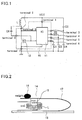
- Fig. 1 is a block diagram of a vibrator controlling circuit according to this invention.
- the vibrator controlling circuit 10 includes a controlling integrated circuit 11, and a MOS transistor 12 which is controlled by it.
- the controlling integrated circuit 11 includes a square wave generating circuit which generates a square wave signal whose generated frequency varies according to the value of an applied voltage and a frequency shift detecting circuit for detecting a shift in the vibrating frequency between the square wave generating circuit and the vibrator.
- a terminal 1 of the controlling integrated circuit 11 is supplied with a power supply voltage VCC, and a coil L of the vibrator 14 is connected between the terminals 1 and 2.
- a terminal 3 is connected to capacitors C2 and C4.
- Terminals 4 and 5 are connected to a resistor R2 and a capacitor C3 which define the generated frequency of the square wave generating circuit.
- a terminal 6 is connected to a capacitor C1.
- a terminal 7 is connected to ground.
- a capacitor C5 is connected between terminals 2 and 8.
- the vibrator 14 includes an iron core 15, a flat spring 17 equipped with the iron core 15 and a weight 16, and a coil L wound around the iron core 15.
- the one end of the flat spring 17 is fixed to a base 18.
- a power supply voltage VCC is applied to the vibrator control circuit 10. Then, the square wave generating circuit in the controlling integrated circuit 11 starts to operate and generates a square wave generating signal at 120 Hz(duty of 50 %).
- the square wave signal taken out from the above controlling integrated circuit 11 is applied to the gate of the MOS transistor 12, the MOS transistor 12 is turned on or off.
- the MOS transistor 12 When the MOS transistor 12 is turned on, the power supply voltage VCC is supplied to the coil L of the vibrator 14 so that a magnetic field is generated to attract the flat spring 17.
- the MOS transistor 12 When the MOS transistor 12 is turned off, the flat spring 17 is restored to the original state because of elastic force. By repetition of such an operation, the weight 16 which is disposed on the flat spring 17 vibrates to inform the user of an arrival of a ringing signal.
- the resonance frequency of the vibrator 14 is about 240 Hz. This resonance frequency varies according to dispersion of elements such as the flat spring 17 or using condition such as using the portable telephone set up or lying down. If the frequency of the square wave signal taken out from the square wave generating circuit of the controlling circuit integrated circuit 11 remains 240 Hz although the resonance frequency of the vibrator 14 has varied, the vibrator 14 weakens or sometimes stops in vibration.
- the frequency shift detecting circuit in the controlling integrated circuit 11 detects a frequency shift between the square wave signal taken out from the square wave generating circuit and the vibrator 14. Using the detected signal, the frequency of the square wave generating circuit is trimmed to the resonance frequency of the resonator 14 so that the vibrator 14 is vibrated sufficiently.
- Fig. 3 is a detailed block diagram of the vibrator controlling circuit 10.
- a square wave signal generating circuit generates a square wave signal whose frequency and duty is determined by resistors R1 and R2 connected to a terminal DIS and a capacitor C3 connected to a terminal CR.
- the square wave signal at 240 Hz with duty of 40 % is generated.
- the potential at the input control terminal CTL of the square wave signal generating circuit 20 is generally set at VCC/2. However, if the potential is set on the side of VCC, the square wave signal has a frequency lower than 240 Hz, whereas if the potential is set on the side of GND, the square wave signal has a frequency higher than 240 Hz.
- An inverter 21 inverts the square wave signal taken out from the terminal Q of the square wave signal generating circuit 20.
- a half-divider 22 half-divides the square signal inverted by the inverter 21 to provide the square wave signal at 120 Hz with duty of 50 %.
- the square wave signal taken out from the half- divider 22 is applied to the gate of the MOS transistor 12 via an inverter 23. It should be noted that a capacitor C5 and a resistor R3 are inserted in order to prevent the ringing of the MOS transistor 12.
- Fig. 4 is a block diagram of the half-divider 22.
- the half-divider 22 has an input terminal IN to which the square wave signal at 240 Hz inverted by the inverter 21 is applied and an output terminal OUT from which the converted square wave signal at 120 Hz is taken out.
- the frequency shift detecting circuit 24 includes an AND circuit 25, an AND circuit 26, a first switching element 27, a second switching element 28 and an operational amplifier 29.
- the input terminals of the AND circuit 25 are connected to an output terminal of said inverter 21, an output terminal of the half-divider 22 and the one end of the coil L, whereas the output terminal thereof is connected to the terminal 3 of the second switching element 28.
- the input terminals of the AND circuit 26 are connected to the input terminal of the inverter 21 and output terminal of the half-divider 22, whereas the output terminal thereof is connected to the terminal 3 of the first switching element 27.
- the terminal (-) of the operational amplifier 29 is connected to the coil L through the first switching element and27 a diode D, whereas the terminal (+) thereof is connected to the coil L through the diode D.
- the output terminal of the operational amplifier 29 is connected to the control terminal CTL of the square wave signal generating circuit 20 through the second switching element 28.
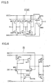
- Fig. 5 is a block diagram of the first switching element 27 and second switching element 28.
- the first switching element includes P channel MOS transistors MP1, MP2, MP3, MP5 and N channel MOS transistors MN1, MN2, MN3 and MN6.
- P channel MOS transistors MP1, MP2, MP3, MP5 P channel MOS transistors MP1, MP2, MP3, MP5 and N channel MOS transistors MN1, MN2, MN3 and MN6.
- Fig. 6 is a block diagram of the operational amplifier 29.
- the operational amplifier 29 includes P channel MOS transistors MP6, MP7, MP8 and N channel MOS transistors MN7, MN8, MN9 and MN10.
- the output terminal OUT provides VCC.
- the output terminal provides GND.
- Fig. 7 is a waveform chart showing the operation of the vibrator controlling circuit 10.
- a square wave signal a at 240 Hz (with on duty of 40 %) is generated from the square wave signal generating circuit 20.
- the square wave signal is inverted by the inverter 21 to provide a square wave signal b .
- the square wave signal b is applied to the input terminal IN of the half-divider 22.
- the square wave signal b is divided into the square wave signal c at 120 Hz (with on-duty of 50 %).
- the square wave signal c at 120 Hz is inverted into a square wave signal f by the inverter 23. Further, a driving waveform g is applied to the gate of the MOS transistor 12 through the capacitor C5 and resistor R3 for preventing ringing. Thus, the MOS transistor 12 repeats ON and OFF.
- the power supply voltage VCC is supplied to the coil L of the vibrator 14, so that a magnetic field is generated to attract the flat spring 17.
- the MOS transistor 12 is turned off, the flat spring 17 is restored to the original state because of elastic force.
- the power supply voltage VCC is supplied to the coil L of the vibrator 14 so that the magnetic field is generated, thereby attracting the flat spring 17.
- the weight 16 vibrates to inform the user of arrival of the ringing signal.
- the driving waveform g is applied to the input terminal 1 of the first switching element 27 as a waveform i through the diode D.
- the terminal 3 of the first switching element 27 is supplied with the square wave signals a and c through the AND circuit 26. Therefore, the input terminal (-) of the operational amplifier 29 is supplied with a waveform j of 0 - 40 % of the driving waveform i through the first switching element 27, whereas the input terminal (+) of the operational amplifier 29 is supplied with the potential of the driving waveform i as it is.
- a waveform k is produced from the output of the operational amplifier 29 and is applied to the second switching element 28.
- the AND-ed signal of the square waveform b , square waveform c and driving waveform h is applied to the terminal 3 of the switching element 28. Therefore, the second switching element 28 transmits 40 - 100 % of the waveform k .
- a waveform m is supplied to the control terminal CTL of the square wave signal generating circuit 20.
- Fig. 8 shows a vibrating waveform signal of the vibrator 14.
- a driving waveform M on the left side is generated.
- a driving waveform S shown at the center, is generated.
- a driving waveform N is generated.
- the waveform N is generated, so that in 0 - 40 % of the square waveform, the input terminal (-) of the operational amplifier 29 is equal to the input terminal (+) thereof. Thus, the output terminal of the operational amplifier 29 is at "L" level. In 40 % - 100 % of the square waveform, the input terminal (+) is higher than the input terminal (-) so that the output signal from the operational amplifier 29 is at "H" level.
- the AND-ed signal of the square waveform b, square waveform c and driving waveform h is applied to the terminal 3 of the switching element 28, so that the second switching element 28 transmits the waveform m which is 40 - 100 % of the waveform k. Therefore, the potential between the capacitors C2 and C4 (the potential at the junction where C2 and C4 are connected to each other) which has been initially VCC/2 is shifted to a high potential side. Then, the potential at the control terminal CTL of the square waveform signal generating circuit 20 is raised, so that the frequency of the generated signal is shifted from 240 Hz to a low frequency.
- the waveform M is generated, so that in 0 - 40 % of the square waveform, the input terminal (-) of the operational amplifier 29 is equal to the input terminal (+) thereof.
- the output terminal of the operational amplifier 29 is at "L" level.
- the level of the waveform j is held by the capacitor C1. Therefore, the input terminal (-) is higher than the input terminal (+), so that the output signal from the operational amplifier 29 is at "L" level.
- the AND-ed signal of the square waveform b , square wave form c and driving signal h is applied to the terminal 3 of the switching element 2.8, so that the second switching element 28 transmits the L level signal which is 40 - 100 % of the waveform k . Therefore, the potential between the capacitors C2 and C4 which has been initially VCC/2 is shifted to the side of GND.
- the potential at the control terminal CTL of the square wave signal generating circuit 20 is lowered, so that the frequency of the generated signal is shifted from 240 Hz to a higher frequency.
- the generating circuit 4 is. turned on to operate by the switch 3 which is connected to a power supply and turned on by a detected signal detected at the ringing detecting circuit 2 when a ringing signal is received by the antenna 1.
- the MOS transistor 5 is turned on or off. In this way, the power supply voltage VCC is intermittently supplied to the vibrator 6 to vibrate it, thereby informing a user of alert.
- the ringing signal detecting circuit detects the ringing signal and turns on the switch 3 which is connected to a power supply circuit, so that a power switch is required and it further must have a large current capacity since a current from the power supply runs through the switch 3.
- a CONT terminal is installed in said vibrator controlling circuit 10. And a CONT signal, which is changed from "L" level (or “H” level) to "H" level (or “L” level if previously at “L” level) upon a reception of a ringing signal at the ringing signal detecting circuit 2, is applied to said CONT terminal.
- said CONT signal is changed to "H” level (or to "L”level)
- said vibrator controlling circuit is operated to generate a square wave signal of 120Hz.
- the MOS transistor 12 is turned on or off with the square wave signal of 120Hz to vibrate the vibrator 14, so that said power switch is made unnecessary.
- CONT terminals are installed to the square wave generating circuit 20, the half-divider 22 and operational amplifier 29, respectively.
- said CONT signal detected from said ringing signal detecting circuit 2 is at "L" level, so that the CONT terminals of said square wave generating circuit 20, the half-divider 22 and the operational amplifier 29 are set to "L” level.
- all of a terminal Q, a terminal DIS and a terminal CR of said square wave generating circuit 20 are fixed to "H” level.
- a terminal OUT of the half-divider 22 is fixed to "H” level, while an output terminal of the operational amplifier 29 is fixed to "L” level.
- the CONT signal which is supplied by said ringing signal detecting circuit 2 and applied to the CONT terminal of the vibrator controlling circuit 10, becomes "H” level. If the CONT signal, which is applied to the CONT terminal of the vibrator controlling circuit 10, becomes "H” level, the CONT terminals of said square wave generating circuit 20, half-divider 22 and operational amplifier 29 become “H” level as well, and turns to a normal operation status.
- a square wave signal a of 240Hz is generated and outputted from a terminal Q of the square wave generating circuit 20, as described earlier.
- Said square wave signal a is half-divided into a square wave signal c of 120Hz (duty 50%) by the half-divider 22.
- Said square wave signal c of 120Hz is inverted to a square wave switching signal f by an inverter 23, and said signal f goes through a capacitor C5 and a resistor R3 to suppress a ringing, and then is applied to the gate of the MOS transistor 12 as a driving waveform g.
- said MOS transistor 12 repeats switching on and off.
- an operational amplifier 29 of a frequency shift detecting circuit is in an operation status. Accordingly, said driving waveform g , after passing through a diode D, is applied to an input terminal (-) of the operational amplifier 29, and at the same time is applied to an input terminal (+) of the operational amplifier 29 directly after passing the diode D.
- a frequency shift detection signal is detected, and a frequency shift of square wave signal generation is adjusted.
- the vibrator controlling circuit includes a square wave generating circuit for generating a square wave signal whose frequency changes according to the value of a voltage applied to a controlling terminal; a MOS transistor which is turned on/off on the basis of said square wave controlling signal to supply a driving current to a vibrator; and a frequency shift detecting circuit for detecting a shift between the square wave signal of said square wave generating circuit and a resonance frequency of said vibrator.
- a shift in the frequency generated by said square wave generating circuit is trimmed by a signal detected by said frequency shift detecting circuit. In this way, the shift between the resonance frequency of the vibrator and the frequency of the square waveform is always trimmed so that the vibrator can be vibrated sufficiently to inform the user of arrival of a ringing signal.
Landscapes
- Engineering & Computer Science (AREA)
- Mechanical Engineering (AREA)
- Apparatuses For Generation Of Mechanical Vibrations (AREA)
- Oscillators With Electromechanical Resonators (AREA)
Abstract
Description
a second switching element for passing an output signal from the operational amplifier to be supplied to a CTL terminal of the square wave generating circuit, and wherein the first switching element is ON during 0 - 40 % of the square wave signal, the second switching element is ON during 40 - 100 % of the square wave signal, and 0 - 40 % and 40 % - 100 % of the vibrating wave signal are compared with each other.
Claims (9)
- A vibrator controlling circuit comprising:a square wave generating circuit for generating a square wave signal whose frequency changes according to the value of a voltage applied to a controlling terminal;a switching element which is turned on/off on the basis of said square wave signal to supply a driving current to a vibrator; anda frequency shift detecting circuit for detecting a frequency shift between the square wave signal from said square wave generating circuit and a resonance frequency of said vibrator, whereina shift in the frequency generated by said square wave generating circuit is trimmed in accordance with a signal detected by said frequency shift detecting circuit.
- A vibrator controlling circuit according to claim 1, wherein said switching element is a MOS transistor.
- A vibrator controlling circuit according to claim 1 or 2, wherein the square wave signal generated by said square wave generating circuit is divided by a half-divider and the divided signal is applied to said switching element.
- A vibrator controlling circuit according to claim 1, 2 or 3, wherein said frequency shift detecting circuit includes a first switching element for switching a vibrating wave signal from saidvibrator; an operational amplifier with the one input terminal supplied with a signal passed said first switching element and the other terminal supplied with the vibrating wave signal as it is; and a second switching element for passing an output signal from said operational amplifier to be supplied to a CTL terminal of said square wave generating circuit.
- A vibrator controlling circuit according to claim 4, wherein said first switching element is ON during 0 - 40 % of said square wave signal, said second switching element is ON during 40 - 100 % of said square wave signal, and 0 - 40 % and 40 % - 100 % of said vibrating wave signal are compared with each other.
- A vibrator controlling circuit according to any one of the preceding claims, wherein said square wave generating circuit, switching element and frequency shift detecting circuit are constructed of a single chip.
- A vibrator controlling circuit according to Claim 1, 2 or 6, wherein said square wave generating circuit further comprises a CONT terminal, a CONT signal supplied to the CONT terminal turns on the square wave generating circuit when the CONT signal changes from a first level to a second level upon a detection of a ringing signal.
- A vibrator controlling circuit according to Claim 3 or 6, wherein said half-divider further comprises a CONT terminal, a CONT signal supplied to the CONT terminal turns on the half-divider when the CONT signal changes from a first level to a second level upon a detection of a ringing signal.
- A vibrator controlling circuit according to Claim 4, 5 or 6, wherein said operational amplifier in said frequency shift detecting circuit further comprises a CONT terminal, a CONT signal supplied to the CONT terminal turns on the operational amplifier when the CONT signal changes from a first level to a second level upon a detection of a ringing signal.
Applications Claiming Priority (4)
| Application Number | Priority Date | Filing Date | Title |
|---|---|---|---|
| JP2000397717A JP3885927B2 (en) | 2000-12-27 | 2000-12-27 | Vibrator control circuit |
| JP2000397717 | 2000-12-27 | ||
| JP2001109557A JP2002301431A (en) | 2001-04-09 | 2001-04-09 | Vibrator control circuit |
| JP2001109557 | 2001-04-09 |
Publications (3)
| Publication Number | Publication Date |
|---|---|
| EP1220177A2 true EP1220177A2 (en) | 2002-07-03 |
| EP1220177A3 EP1220177A3 (en) | 2003-05-28 |
| EP1220177B1 EP1220177B1 (en) | 2005-11-09 |
Family
ID=26606844
Family Applications (1)
| Application Number | Title | Priority Date | Filing Date |
|---|---|---|---|
| EP01310896A Expired - Lifetime EP1220177B1 (en) | 2000-12-27 | 2001-12-27 | Vibrator controlling circuit |
Country Status (4)
| Country | Link |
|---|---|
| US (1) | US6897766B2 (en) |
| EP (1) | EP1220177B1 (en) |
| CN (1) | CN1254988C (en) |
| DE (1) | DE60114758T2 (en) |
Families Citing this family (10)
| Publication number | Priority date | Publication date | Assignee | Title |
|---|---|---|---|---|
| US7421264B2 (en) * | 2002-10-29 | 2008-09-02 | Motorola, Inc. | Device and method for reducing vibration effects on position measurement |
| WO2014186776A1 (en) * | 2013-05-17 | 2014-11-20 | Cirrus Logic, Inc. | Charge pump-based circuitry for bjt power supply |
| WO2014186765A1 (en) | 2013-05-17 | 2014-11-20 | Cirrus Logic, Inc. | Single pin control of bipolar junction transistor (bjt)-based power stage |
| WO2015017317A2 (en) | 2013-07-29 | 2015-02-05 | Cirrus Logic, Inc. | Two terminal drive of bipolar junction transistor (bjt) for switch-mode operation of a light emitting diode (led)-based bulb |
| WO2015017315A1 (en) | 2013-07-29 | 2015-02-05 | Cirrus Logic, Inc. | Compensating for a reverse recovery time period of a bipolar junction transistor (bjt) in switch-mode operation of a light-emitting diode (led)-based bulb |
| US9504118B2 (en) | 2015-02-17 | 2016-11-22 | Cirrus Logic, Inc. | Resistance measurement of a resistor in a bipolar junction transistor (BJT)-based power stage |
| US9603206B2 (en) | 2015-02-27 | 2017-03-21 | Cirrus Logic, Inc. | Detection and control mechanism for tail current in a bipolar junction transistor (BJT)-based power stage |
| US9609701B2 (en) | 2015-02-27 | 2017-03-28 | Cirrus Logic, Inc. | Switch-mode drive sensing of reverse recovery in bipolar junction transistor (BJT)-based power converters |
| US12207880B2 (en) | 2018-07-02 | 2025-01-28 | Nidek Co., Ltd. | Ultrasonic tonometer |
| CN116430073B (en) * | 2022-09-23 | 2023-11-10 | 上海铁路通信有限公司 | Gear speed sensor output frequency test circuit |
Family Cites Families (7)
| Publication number | Priority date | Publication date | Assignee | Title |
|---|---|---|---|---|
| US4395665A (en) * | 1981-06-09 | 1983-07-26 | The Arthur G. Russell Company, Incorporated | Control system for vibrating a member at its resonant frequency |
| US5396516A (en) * | 1993-02-22 | 1995-03-07 | Qualcomm Incorporated | Method and system for the dynamic modification of control paremeters in a transmitter power control system |
| US5436622A (en) * | 1993-07-06 | 1995-07-25 | Motorola, Inc. | Variable frequency vibratory alert method and structure |
| JPH09117721A (en) * | 1994-09-28 | 1997-05-06 | Seiko Instr Inc | Vibration module |
| AUPO224596A0 (en) * | 1996-09-11 | 1996-10-03 | Robert Bosch Gmbh | A siren control system |
| US5936516A (en) * | 1997-01-31 | 1999-08-10 | Motorola, Inc. | Vibrating apparatus and method therefor |
| US6057753A (en) * | 1997-07-03 | 2000-05-02 | Projects Unlimited, Inc. | Vibrational transducer |
-
2001
- 2001-12-27 US US10/032,936 patent/US6897766B2/en not_active Expired - Fee Related
- 2001-12-27 CN CNB011440414A patent/CN1254988C/en not_active Expired - Fee Related
- 2001-12-27 DE DE60114758T patent/DE60114758T2/en not_active Expired - Fee Related
- 2001-12-27 EP EP01310896A patent/EP1220177B1/en not_active Expired - Lifetime
Also Published As
| Publication number | Publication date |
|---|---|
| EP1220177B1 (en) | 2005-11-09 |
| EP1220177A3 (en) | 2003-05-28 |
| CN1254988C (en) | 2006-05-03 |
| DE60114758T2 (en) | 2006-07-20 |
| US20020082056A1 (en) | 2002-06-27 |
| US6897766B2 (en) | 2005-05-24 |
| CN1364046A (en) | 2002-08-14 |
| DE60114758D1 (en) | 2005-12-15 |
Similar Documents
| Publication | Publication Date | Title |
|---|---|---|
| US5570004A (en) | Supply voltage regulator and an electronic apparatus | |
| EP0888032B1 (en) | Electro-mechanical-acoustic transducing arrangement | |
| JP4269518B2 (en) | Electro-mechanical-acoustic transducer and electro-mechanical-acoustic transducer using the same | |
| EP1220177B1 (en) | Vibrator controlling circuit | |
| JP2001501526A (en) | Mode tracking transducer driver for nonlinear transducer | |
| JPH06503188A (en) | Drive circuit with weighted transducer and feedback mechanism | |
| JPH0215418Y2 (en) | ||
| JP2002157030A (en) | Stabilized DC power supply | |
| EP1385262B1 (en) | Mobile terminal with electromagnetic actuator | |
| CN108136442B (en) | Piezo Actuator Drive Circuit | |
| JP3885927B2 (en) | Vibrator control circuit | |
| JP3263632B2 (en) | Communication equipment and its adjusting device | |
| US5635788A (en) | Control circuit for a piezoelectric vibrator | |
| EP1355280B1 (en) | Vibrator controlling circuit | |
| JP4274520B2 (en) | Oscillation amplitude detection circuit, oscillation circuit, and integrated circuit for oscillation | |
| JP2002301431A (en) | Vibrator control circuit | |
| JPH03274832A (en) | Buzzer/alarm switching device | |
| JP2001326988A (en) | Driving circuit for electroacoustic transducer and driving method thereof | |
| CN2109035U (en) | Contectless electric loudspeaker | |
| JPH03248635A (en) | Selective call receiver | |
| JPH09265593A (en) | Alarm sound device | |
| JPS63174414A (en) | Oscillation circuit | |
| JPH07162229A (en) | Oscillator circuit | |
| KR20020090041A (en) | Vibration apparatus for mobile telecommunication terminal | |
| JPS63187752A (en) | Tone ringer driving circuit device for telephone set |
Legal Events
| Date | Code | Title | Description |
|---|---|---|---|
| PUAI | Public reference made under article 153(3) epc to a published international application that has entered the european phase |
Free format text: ORIGINAL CODE: 0009012 |
|
| AK | Designated contracting states |
Kind code of ref document: A2 Designated state(s): AT BE CH CY DE DK ES FI FR GB GR IE IT LI LU MC NL PT SE TR |
|
| AX | Request for extension of the european patent |
Free format text: AL;LT;LV;MK;RO;SI |
|
| PUAL | Search report despatched |
Free format text: ORIGINAL CODE: 0009013 |
|
| AK | Designated contracting states |
Designated state(s): AT BE CH CY DE DK ES FI FR GB GR IE IT LI LU MC NL PT SE TR |
|
| AX | Request for extension of the european patent |
Extension state: AL LT LV MK RO SI |
|
| RIC1 | Information provided on ipc code assigned before grant |
Ipc: 7B 06B 1/02 B Ipc: 7B 06B 1/04 B Ipc: 7G 08B 6/00 A |
|
| 17P | Request for examination filed |
Effective date: 20030912 |
|
| AKX | Designation fees paid |
Designated state(s): DE FI FR GB |
|
| 17Q | First examination report despatched |
Effective date: 20040211 |
|
| GRAP | Despatch of communication of intention to grant a patent |
Free format text: ORIGINAL CODE: EPIDOSNIGR1 |
|
| GRAS | Grant fee paid |
Free format text: ORIGINAL CODE: EPIDOSNIGR3 |
|
| GRAA | (expected) grant |
Free format text: ORIGINAL CODE: 0009210 |
|
| AK | Designated contracting states |
Kind code of ref document: B1 Designated state(s): DE FI FR GB |
|
| REG | Reference to a national code |
Ref country code: GB Ref legal event code: FG4D |
|
| REF | Corresponds to: |
Ref document number: 60114758 Country of ref document: DE Date of ref document: 20051215 Kind code of ref document: P |
|
| ET | Fr: translation filed | ||
| PLBE | No opposition filed within time limit |
Free format text: ORIGINAL CODE: 0009261 |
|
| STAA | Information on the status of an ep patent application or granted ep patent |
Free format text: STATUS: NO OPPOSITION FILED WITHIN TIME LIMIT |
|
| 26N | No opposition filed |
Effective date: 20060810 |
|
| PGFP | Annual fee paid to national office [announced via postgrant information from national office to epo] |
Ref country code: FI Payment date: 20071213 Year of fee payment: 7 |
|
| PGFP | Annual fee paid to national office [announced via postgrant information from national office to epo] |
Ref country code: FR Payment date: 20071210 Year of fee payment: 7 Ref country code: GB Payment date: 20071227 Year of fee payment: 7 |
|
| PGFP | Annual fee paid to national office [announced via postgrant information from national office to epo] |
Ref country code: DE Payment date: 20071220 Year of fee payment: 7 |
|
| PG25 | Lapsed in a contracting state [announced via postgrant information from national office to epo] |
Ref country code: FI Free format text: LAPSE BECAUSE OF NON-PAYMENT OF DUE FEES Effective date: 20081227 |
|
| GBPC | Gb: european patent ceased through non-payment of renewal fee |
Effective date: 20081227 |
|
| REG | Reference to a national code |
Ref country code: FR Ref legal event code: ST Effective date: 20090831 |
|
| PG25 | Lapsed in a contracting state [announced via postgrant information from national office to epo] |
Ref country code: DE Free format text: LAPSE BECAUSE OF NON-PAYMENT OF DUE FEES Effective date: 20090701 |
|
| PG25 | Lapsed in a contracting state [announced via postgrant information from national office to epo] |
Ref country code: GB Free format text: LAPSE BECAUSE OF NON-PAYMENT OF DUE FEES Effective date: 20081227 |
|
| PG25 | Lapsed in a contracting state [announced via postgrant information from national office to epo] |
Ref country code: FR Free format text: LAPSE BECAUSE OF NON-PAYMENT OF DUE FEES Effective date: 20081231 |