EP1220105B1 - Interface apparatus and method thereof for display system - Google Patents
Interface apparatus and method thereof for display system Download PDFInfo
- Publication number
- EP1220105B1 EP1220105B1 EP01127461A EP01127461A EP1220105B1 EP 1220105 B1 EP1220105 B1 EP 1220105B1 EP 01127461 A EP01127461 A EP 01127461A EP 01127461 A EP01127461 A EP 01127461A EP 1220105 B1 EP1220105 B1 EP 1220105B1
- Authority
- EP
- European Patent Office
- Prior art keywords
- data
- display system
- byte
- displaying
- mode
- Prior art date
- Legal status (The legal status is an assumption and is not a legal conclusion. Google has not performed a legal analysis and makes no representation as to the accuracy of the status listed.)
- Expired - Lifetime
Links
Images





Classifications
-
- G—PHYSICS
- G06—COMPUTING OR CALCULATING; COUNTING
- G06F—ELECTRIC DIGITAL DATA PROCESSING
- G06F13/00—Interconnection of, or transfer of information or other signals between, memories, input/output devices or central processing units
- G06F13/38—Information transfer, e.g. on bus
- G06F13/40—Bus structure
- G06F13/4063—Device-to-bus coupling
- G06F13/4068—Electrical coupling
- G06F13/4086—Bus impedance matching, e.g. termination
-
- H—ELECTRICITY
- H04—ELECTRIC COMMUNICATION TECHNIQUE
- H04M—TELEPHONIC COMMUNICATION
- H04M1/00—Substation equipment, e.g. for use by subscribers
- H04M1/72—Mobile telephones; Cordless telephones, i.e. devices for establishing wireless links to base stations without route selection
- H04M1/724—User interfaces specially adapted for cordless or mobile telephones
- H04M1/72403—User interfaces specially adapted for cordless or mobile telephones with means for local support of applications that increase the functionality
- H04M1/72427—User interfaces specially adapted for cordless or mobile telephones with means for local support of applications that increase the functionality for supporting games or graphical animations
-
- G—PHYSICS
- G09—EDUCATION; CRYPTOGRAPHY; DISPLAY; ADVERTISING; SEALS
- G09G—ARRANGEMENTS OR CIRCUITS FOR CONTROL OF INDICATING DEVICES USING STATIC MEANS TO PRESENT VARIABLE INFORMATION
- G09G3/00—Control arrangements or circuits, of interest only in connection with visual indicators other than cathode-ray tubes
- G09G3/20—Control arrangements or circuits, of interest only in connection with visual indicators other than cathode-ray tubes for presentation of an assembly of a number of characters, e.g. a page, by composing the assembly by combination of individual elements arranged in a matrix no fixed position being assigned to or needed to be assigned to the individual characters or partial characters
- G09G3/34—Control arrangements or circuits, of interest only in connection with visual indicators other than cathode-ray tubes for presentation of an assembly of a number of characters, e.g. a page, by composing the assembly by combination of individual elements arranged in a matrix no fixed position being assigned to or needed to be assigned to the individual characters or partial characters by control of light from an independent source
- G09G3/36—Control arrangements or circuits, of interest only in connection with visual indicators other than cathode-ray tubes for presentation of an assembly of a number of characters, e.g. a page, by composing the assembly by combination of individual elements arranged in a matrix no fixed position being assigned to or needed to be assigned to the individual characters or partial characters by control of light from an independent source using liquid crystals
-
- Y—GENERAL TAGGING OF NEW TECHNOLOGICAL DEVELOPMENTS; GENERAL TAGGING OF CROSS-SECTIONAL TECHNOLOGIES SPANNING OVER SEVERAL SECTIONS OF THE IPC; TECHNICAL SUBJECTS COVERED BY FORMER USPC CROSS-REFERENCE ART COLLECTIONS [XRACs] AND DIGESTS
- Y02—TECHNOLOGIES OR APPLICATIONS FOR MITIGATION OR ADAPTATION AGAINST CLIMATE CHANGE
- Y02D—CLIMATE CHANGE MITIGATION TECHNOLOGIES IN INFORMATION AND COMMUNICATION TECHNOLOGIES [ICT], I.E. INFORMATION AND COMMUNICATION TECHNOLOGIES AIMING AT THE REDUCTION OF THEIR OWN ENERGY USE
- Y02D10/00—Energy efficient computing, e.g. low power processors, power management or thermal management
-
- Y—GENERAL TAGGING OF NEW TECHNOLOGICAL DEVELOPMENTS; GENERAL TAGGING OF CROSS-SECTIONAL TECHNOLOGIES SPANNING OVER SEVERAL SECTIONS OF THE IPC; TECHNICAL SUBJECTS COVERED BY FORMER USPC CROSS-REFERENCE ART COLLECTIONS [XRACs] AND DIGESTS
- Y02—TECHNOLOGIES OR APPLICATIONS FOR MITIGATION OR ADAPTATION AGAINST CLIMATE CHANGE
- Y02D—CLIMATE CHANGE MITIGATION TECHNOLOGIES IN INFORMATION AND COMMUNICATION TECHNOLOGIES [ICT], I.E. INFORMATION AND COMMUNICATION TECHNOLOGIES AIMING AT THE REDUCTION OF THEIR OWN ENERGY USE
- Y02D30/00—Reducing energy consumption in communication networks
- Y02D30/70—Reducing energy consumption in communication networks in wireless communication networks
Definitions
- an object of the present invention to provide an interface apparatus and a method thereof for a display system which are capable of minimizing a quantity of power consumption in a standby state of a display system by displaying an image (an animation, a still image and a text) and a text through an I2C (IIC) interface of a main CPU by not operating a video codec in a standby mode of the display system.
- an image an animation, a still image and a text
- IIC I2C
- an interface method for a display system includes outputting data including an image and a text, being inputted the data through an I2C interface in a standby mode and displaying the image and text on a screen, and being inputted the data through a video codec in an active mode and displaying the image and text on the screen.
- an interface apparatus of a LCD system in accordance with the present invention includes a main CPU (Central Processing Unit) 11 outputting data having an image (still image, moving picture, animation) and a text to a LCD driver 13 through a video codec 12 in an active mode of a LCD system and outputting pertinent data (data having an image or a text, etc) to the LCD driver 13 by using an I2C interface in a standby mode of the LCD system, a video codec 12 being inputted data having a still image, a moving picture, an animation, a text from the CPU 11 and outputting it to the LCD driver 13 in the active mode, and a LCD driver 13 being inputted data through the video codec 12 in the active mode, displaying the image and text on a screen of the LCD, being directly inputted the data from the main CPU 11 in the standby mode and displaying the image and text of the data on the screen of the LCD.
- a main CPU Central Processing Unit
- the image/text type (1bit) describes whether transmitted data is image data or text data.
- Image data is constructed as 3 bit
- text data is constructed as1 bit.
- Figure 5 is a block diagram illustrating a memory unit for an animation mode in accordance with the present invention.
- the still image data and text data stored in the OSD memories 62, 63 are displayed on the screen of the LCD as an overlay format through an overlay processing unit 64.
- a method for adjusting the control register is used in a command about the overlay. For example, when data is recorded on the one text memory, data of the other memory is read and is displayed on the screen of the LCD.
- data to be written is the last data of a frame, by setting the EOFD bit as "1"
- the display controller reads the pertinent data and informs that the pertinent data can be displayed on the screen of the LCD.
- Figure 7 is a block diagram illustrating a memory for a text display mode.
- each OSD memory illustrated in Figures 5 ⁇ 7 is all same OSD memory, however it has different reference numeral according to the operation type (mode).
- Figures 8E ⁇ 8H illustrate examples of a format for writing text data.
- a write method of burst data will be described with reference to accompanying Figure 8E .
- the LCD system in accordance with the present invention is for reducing power consumption of the display system
- the present invention is not limited to the LCD system, it can be used for a display apparatus such as an organic electroluminescence, etc.
Landscapes
- Engineering & Computer Science (AREA)
- Theoretical Computer Science (AREA)
- General Engineering & Computer Science (AREA)
- Physics & Mathematics (AREA)
- Computer Hardware Design (AREA)
- General Physics & Mathematics (AREA)
- Computer Networks & Wireless Communication (AREA)
- Human Computer Interaction (AREA)
- Signal Processing (AREA)
- Chemical & Material Sciences (AREA)
- Crystallography & Structural Chemistry (AREA)
- Control Of Indicators Other Than Cathode Ray Tubes (AREA)
- Liquid Crystal Display Device Control (AREA)
- Digital Computer Display Output (AREA)
- Transforming Electric Information Into Light Information (AREA)
- Controls And Circuits For Display Device (AREA)
Description
- The present invention relates to an interface apparatus and a method thereof for a display system, and in particular to an interface apparatus and a method thereof for a display system which are capable of displaying an image and a text on a screen of a LCD (liquid crystal display) and minimizing a power consumption when a LCD (liquid crystal display) system is in a standby state.
-
US-A-5 822 720 discloses a system and method for linking streams of multimedia data for reference material for display. The system for indexing displayed elements is useful for accessing and understanding new materials in which a user highlights unknown words or displayed elements encountered while viewing displayed materials. Readings for all words are readily viewable for any selected word as well as an English reference to the selected word or phrase. An indexing scheme allows word-by-word access to any of several external multi-media references.WO/00 38340 A - Generally, a LCD (liquid crystal system) system such as an .IMT-2000 (international mobile telecommunications 2000) compressing video data, restoring it and displaying it on a screen of a LCD is constructed with a main CPU (central processing unit), a video codec and a LCD (liquid crystal display) driver. Herein, the LCD system is operated as an active mode, a standby mode and a power down mode. The active mode means a normal operation mode, the standby mode means a standby state, and the power down mode means a state displaying nothing on a screen of a LCD but being ready for a display.
- However, because the LCD system according to the prior art operates a video codec in a standby mode, it consumes lots of power unnecessarily. In more detail, when the video codec is operated in the standby mode of the LCD system in accordance with the prior art, power is unnecessarily consumed 20 times larger than the power consumption when the video codec is not operated.
- Accordingly, it is an object of the present invention to provide an interface apparatus and a method thereof for a display system which are capable of minimizing a quantity of power consumption in a standby state of a display system by displaying an image (an animation, a still image and a text) and a text through an I2C (IIC) interface of a main CPU by not operating a video codec in a standby mode of the display system.
- In order to achieve the above-mentioned object, an interface method for a display system includes outputting data including an image and a text, being inputted the data through an I2C interface in a standby mode and displaying the image and text on a screen, and being inputted the data through a video codec in an active mode and displaying the image and text on the screen.
- In order to achieve the above-mentioned object, an interface apparatus for a display system includes a main CPU outputting data including an image and a text according to an operation mode of a system, a video codec being inputted the data and outputting it by interfacing with the main CPU according to the operation mode, and a driver being inputted the data through the video codec or being inputted the data from the main CPU through the I2C interface in accordance with the operation mode and displaying the image and text on the screen.
- In order to achieve the above-mentioned object, in a method transmitting data to a memory of a LCD (liquid crystal display) driver through an I2C interface of a main CPU of a mobile communication terminal and writing the data, an interface method for a display system includes outputting sequentially a byte for slave address, a byte for mode setting and a byte for pixel data when the data is burst data, outputting sequentially a byte for slave address, a byte for mode setting, a byte for area start address, a byte for area end address and a byte for pixel data when the data is area data, outputting sequentially a byte for slave address, a byte for mode setting, a byte for line address, a byte for pixel data when the data is line data, and outputting sequentially a byte for slave address, a byte for mode setting, a byte for pixel address and a byte for pixel data when the data is pixel data in order to write the data in the memory.
-
-
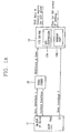
Figure 1A is a block diagram illustrating an interface apparatus of a LCD (liquid crystal display) system in accordance with the present invention; -
Figure 1B illustrates an operation mode and a display scheme in accordance with the present invention; -
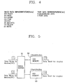
Figure 2 is a block diagram illustrating a memory unit in accordance with the present invention; -
Figure 3 is a format view illustrating a mode setting in accordance with the present invention; -
Figure 4 illustrates an expression example about each data in accordance with the present invention; -
Figure 5 is a block diagram illustrating a memory unit for an animation mode in accordance with the present invention; -
Figure 6 is a block diagram illustrating a memory for a still image and a text display mode; -
Figure 7 is a block diagram illustrating a memory only for a text display mode; -
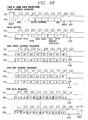
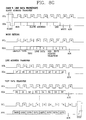
Figures 8A ∼ 8H illustrate data formats about a method for writing data in OSD memories according to control of a main CPU of a LCD system; and -
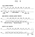
Figure 9 is a write format view illustrating register control data in order to describe a method for writing register control data. - Hereinafter, preferred embodiments of an interface apparatus and a method thereof for a LCD (liquid crystal display) system in accordance with the present invention which are capable of displaying an image (animation, still image, text) and a text on a screen of a LCD (liquid crystal display) through an I2C (IIC) interface of a main CPU without operating a video codec in a standby mode will be described in detail with reference to accompanying
Figures 1 ∼ 9 . -
Figure 1A is a block diagram illustrating an interface apparatus of a LCD system in accordance with the present invention. - As depicted in
Figure 1 , an interface apparatus of a LCD system in accordance with the present invention includes a main CPU (Central Processing Unit) 11 outputting data having an image (still image, moving picture, animation) and a text to aLCD driver 13 through avideo codec 12 in an active mode of a LCD system and outputting pertinent data (data having an image or a text, etc) to theLCD driver 13 by using an I2C interface in a standby mode of the LCD system, avideo codec 12 being inputted data having a still image, a moving picture, an animation, a text from theCPU 11 and outputting it to theLCD driver 13 in the active mode, and aLCD driver 13 being inputted data through thevideo codec 12 in the active mode, displaying the image and text on a screen of the LCD, being directly inputted the data from themain CPU 11 in the standby mode and displaying the image and text of the data on the screen of the LCD. First, the LCD system is operated as three modes such as an active mode, a standby mode and a power down mode. The operation of the interface apparatus for the LCD system in accordance with the present invention will be described in detail with reference to accompanyingFigures 1B ∼ 9 . -
Figure 1B illustrates an operation mode and a display scheme in accordance with the present invention. In more detail,Figure 1B illustrates the operation of the three modes (active mode, standby mode, power down mode) and the display scheme. - As depicted in
Figure 1B , themain CPU 11, thevideo codec 12 and theLCD driver 13 operate normally in the active mode. Herein, data such as an image (a still image, a moving picture, an animation) and a text, etc. is inputted to theLCD driver 13 through thevideo codec 12 at 30 frames per second, and theLCD driver 13 displays the inputted data on the screen of the LCD at 30 frames per second. - The standby mode is set when a key signal is not inputted for a certain time. Herein, a text can be displayed with a simple animation or still image as a background or only text can be displayed in the standby mode. Instead of it, the
main CPU 11 transmits the data to theLCD driver 13 at 5 frames per second by using the I2C interface and stores it in a memory unit (example: SRAM) 13B of theLCD driver 13, and aLCD controller 13A of theLCD driver 13 displays the data stored in thememory unit 13B on the screen of the LCD at 5 frames per second. - The power down mode means nothing is displayed on the screen of the LCD but the LCD system is ready for displaying.
-
Figure 2 is a block diagram illustrating the memory unit in accordance with the present invention. In more detail,Figure 2 is a block diagram illustrating the memory of theLCD driver 13. - As depicted in
Figure 2 , theLCD driver 13 stores the data (serial data) transmitted from the main CPU11 through the I2C interface in aserial buffer 21 first and stores it in OSD (on screen display)memories main CPU 11 writes data in theOSD memory 22, theLCD controller 13A reads pre-stored data from theother OSD memory 23 and displays it on the screen of the LCD, accordingly delay in the data output is not occurred by the read/write operations of thememories - For reference, by considering 176 × 220 (1 pixel is constructed with three elements respectively describing R, G, B colors) pixel acknowledged by a provisional usage of a LCD panel for an IMT-2000 terminal, a memory of 176 × 220 × 3bit as a size of one frame is used as the
OSD memories LCD controller 13A, when the display operation is performed, a clock signal outputted from an oscillator (not shown) of theLCD driver 13 is used. - In the meantime, the clock signal is used in mode setting of 1 byte of data transmitted once in the I2C interfacing between the
main CPU 11 and theLCD driver 13. The mode setting will now be described in detail with reference to accompanyingFigure 3 . -
Figure 3 is a format view illustrating a mode setting in accordance with the present invention. - As depicted in
Figure 3 , the mode setting is classified into a display type (2bit), an image/text type (1bit), a data type (1bit), an OSD memory selection bit (1 bit) and an EOFD (end of frame data) (1bit). - First, the display type (2bit) describes a kind of data to be played. The kind of data to be displayed is largely divided into an animation display, a text display with a still image background, only text display and a mode for register control for a LCD controller. In more detail, the memory of the
LCD driver 13 is allocated according to the display type. Herein, by saving power of unused memory cells, a quantity of power consumption can be reduced. The memory allocation according to the display type will be described in detail with reference to accompanyingFigures 5 ∼ 7 . - The image/text type (1bit) describes whether transmitted data is image data or text data. Image data is constructed as 3 bit, and text data is constructed as1 bit.
- The data type (1bit) describes a type of data, data type is largely divided into burst data, area data, line data and pixel data. Data write stream in accordance with the data type will be described in detail with reference to accompanying
Figures 8A ∼ 8H . - The OSD memory selection bit (1bit) is for making the
main CPU 11 select each of two OSD memories of theLCD driver 13. The EOFD (end of frame data) (1bit) is for notifying the end of frame data. In more detail, the EOFD (1bit) is for coinciding a synchronous of time write data in thememory unit 13B with a time for reading contents stored in thememory unit 13B by themain CPU 11 and displaying it by theLCD controller 13A. When themain CPU 11 shows the EOF (end of frame) with the written data, themain CPU 11 does not access to the pertinent memory for a preset certain time, and for the preset certain time theLCD controller 13A reads updated data of the memory by themain CPU 11 and displays it on the screen of the LCD. -
Figure 4 illustrates an expression example about each data in accordance with the present invention. - As depicted in
Figure 4 ,3 bit image data describes 8 colors. In text data of 1 bit, "0' means a background data, "1" means text data, it is possible to select a color of background data and text data by using register control data as shown atFigure 9 . -
Figure 5 is a block diagram illustrating a memory unit for an animation mode in accordance with the present invention. - As depicted in
Figure 5 , both twomemories LCD driver 13 are used. As described above, when themain CPU 11 writes data in theOSD memory 52, data pre-stored in theother OSD memory 53 is read and displayed on the screen of the LCD. When present recording data is the last data of a frame, by setting the EOFD bit as "1", a display controller (not shown) reads the pertinent data and informs that the pertinent data can be displayed on the screen of the LCD. -
Figure 6 is a block diagram of a memory for a still image and a text display mode. - As depicted in
Figure 6 , between the twoISD memories LCD driver 13, theOSD memory 62 is used for storing a background still image. Theother OSD memory 63 is divided into three regions, two regions having a size of 176 × 220 × 1bit are selected as text regions, and text data is updated. Unused one regions is operated (set) as a power save mode. - The still image data and text data stored in the
OSD memories overlay processing unit 64. A method for adjusting the control register is used in a command about the overlay. For example, when data is recorded on the one text memory, data of the other memory is read and is displayed on the screen of the LCD. Herein, when data to be written is the last data of a frame, by setting the EOFD bit as "1", the display controller reads the pertinent data and informs that the pertinent data can be displayed on the screen of the LCD. -
Figure 7 is a block diagram illustrating a memory for a text display mode. - As depicted in
Figure 7 , in eachOSD memory main CPU 11 is recorded on the one OSD memory, namely, theOSD memory 72, the text data pre-stored in theother OSD memory 73 is read and displayed on the screen of the LCD. In addition, when the recorded data is the last data of the frame, by setting the EOFD bit as "1", the display controller reads the pertinent data and informs that the pertinent data can be displayed. - For example, each OSD memory illustrated in
Figures 5 ∼ 7 is all same OSD memory, however it has different reference numeral according to the operation type (mode). -
Figures 8A ∼ 8H illustrate data formats about a method for writing data in an OSD memory according to control of a main CPU of a LCD system. In more detail, data is classified into 8 types in which kinds of data to be written is an image or a text and types of data is burst, area, line or pixel. Herein,Figures 8A ∼ 8E illustrate examples of format for writing the image data. Hereinafter, each data write method will be described as below. - First, a write method of burst data will be described with reference to accompanying
Figure 8A . - In the first place, in order to be suitable for an I2C standard, a slave address of a device (the LCD driver 13) is transmitted through a first byte. Because it is writing data, a 8th bit set as "0". A second byte is for transmitting contents about a mode setting. Because transmitted data is image data, an image/text bit is set as "1", and because a write type is a burst type, a data type is set as "00". In this case, because data of one frame is transmitted at one time, the EOFD bit is set as "1". A display type and an OSD memory selection bit are set so as to be corresponded to an access method of the present
main CPU 11. And, 3 bit pixel data is transmitted from a third byte. In more detail, when the number of pixels of the used LCD is 176 × 220, 38720 data are transmitted, and after that, the transmission is stopped (finished). The above-mentioned write method can be used in transmission of an animation display and a still background image. - An area data write method will be described with reference to accompanying
Figure 8B . - As well as
Figure 8A , a slave address of the device is transmitted through a first byte. In case of data writing, a 8th bit is set as "0". As same with the above-mentioned method, a second byte is for transmitting contents about a mode setting, because the transmitted data is image data, an image/text bit is set as "1", and because a write type is an area type, a data type is set as "01". A display type ad an OSD memory selection bit are set so as to be corresponded to a method for accessing to the presentmain CPU 11. A start address of an area is transmitted through a third byte. When the number of pixels of the used LCD is 176 × 220, because 16 bit address exists, a start address of 2 byte is transmitted. The last address of the area is transmitted through a fourth byte. A start address of 2 byte is transmitted. From a fifth byte, pixel data of the selected area is transmitted and stopped. The above-mentioned write method can be used valuably when a small animation image is displayed or some part is updated or a small still image is used as a background. - A write method of line data will be described with reference to accompanying
Figure 8C . As same with the above-mentioned method, the slave address of the device is transmitted through a first byte. It is also writing data, a 8th bit is set as "0". In a second mode setting byte, transmitted data is image data, the image/text bit is set as "1", and because the write type is a line type, data type is set as "10". A line address is transmitted through a third byte, when the number of pixels of the used LCD is 176 × 220, a line address of 8bit is transmitted. From a fourth byte, pixel data is transmitted. The transmission is stopped after transmitting 176 image data describable one line. As depicted inFigure 8B , the above-mentioned write method can be used valuably in partial update of an animation image or a still image. Herein, the update method is selected by a program language according to conditions. - A write method of pixel data will be described with reference to accompanying
Figure 8D . A slave address of the device is transmitted through a first byte. Because it is writing data, a 8th bit is set as "0". In a second mode setting byte, because transmitted data is image data, an image/text bit is set as "1", and because a write type is pixel type, a data type is set as "11". An address of pixel is transmitted through a third byte. When the number of pixels of the used LCD is 176 × 220, because a 16 bit pixel address exists, a 2 byte address is transmitted. Pixel data is transmitted through a fourth byte. It is possible to update up to two image pixels by using a byte. It is determined by the program language whether one pixel is updated or two pixels are updated at the same time. The above-mentioned write method can be used valuably in partial update of an animation image or a still image. - In the meantime,
Figures 8E ∼ 8H illustrate examples of a format for writing text data. First, a write method of burst data will be described with reference to accompanyingFigure 8E . - A slave address of the device is transmitted through a first byte. Because it is writing data, a 8th bit is set as "0". In a second mode setting byte, because transmitted data is text data, an image/text bit is set as "0", and because a write type is a burst type, data type is set as "00". In this case, because data of one frame is transmitted at one time, the EOFD bit is set as "1". Text data is transmitted from a third byte. Each text data is constructed as 1 bit, when the number of pixels of the used LCD is 176 × 220, 38720 text data are transmitted. The above-mentioned write method can be valuably used in update of all text data of one frame.
- A write method of area data will be described with reference to accompanying
Figure 8F . A slave address of the device is transmitted through a first byte. Because it is writing the data, a 8th bit is set as "0". In a second mode setting byte, because transmitted data is text data, an image/text bit is set as "0", and because a write type is an area type, data type is set as "01". A start address of the area is transmitted through a third byte. When the number of pixels of the used LCD is 176 × 220, because 16 bit address exists, a start address of 2 byte is transmitted. The last address of the area is transmitted through a fourth byte. The last address is 2 byte. From a fifth byte, text data of the selected area is transmitted and stopped. In the above-mentioned write method can be variously used in partial update of text data. - A write method of line data will be described with reference to accompanying
Figure 8G . - First, a slave address of the device is transmitted through a first byte. Because it is writing data, a 8th bit is set as "0". In a second mode setting byte, because transmitted data is text data, an image/text bit is set as "0", and because a write type is a line type, a data type set as "10". An address of the line is transmitted through a third byte. When the number of pixels of the used LCD is 176 × 220, 8 bit line address is transmitted. From a fourth byte, text data is transmitted. 176 text data describable one line are transmitted and the transmission is stopped. The above-mentioned write method can be valuably used in partial update of text data as well as the method shown at
Figure 8F . - A write method of pixel data will be described with reference to accompanying
Figure 8H . - First, a slave address of the device is transmitted through a first byte. Because it is writing data, a 8th bit is set as "0". In a second mode setting byte, because transmitted data is text data, an image/text bit is set as "0", and because a write type is a pixel type, a data type is set as "11". An address of the pixel is transmitted through a third byte. When the number of pixels of the used LCD is 176 × 220, because 16 bit pixel address exists, 2 byte address is transmitted. And, text data is transmitted through a fourth byte. Herein, it is possible to update up to 8 text data by using one byte. At this point, the number of updated text data is determined by the program language. The above-mentioned write method can be valuably used in the partial update of text data.
-
Figure 9 is a write format view illustrating register control data in order to describe a method for writing register control data. In more detail, it illustrates a method for writing register control data. - First, an address of the device is transmitted through a first byte. Because it is writing data, a 8th bit is set as "0". A second byte is about a mode setting and an address of a register, in the register control, a first 2 bit is set as "11". And, the
rest 6 bit are used as an address of the control register, in thiscase 64 control registers can exist. And, data to be written is transmitted to the register through a third byte. - By using the control register, a motion (active, standby, power down) mode is set, positions of OSD (on screen display) regions are selected, on/off of the selected OSD regions are determined or colors of a text and a background in the regions are selected. For reference, the rest control registers are selected after due consultation with manufactures of the
LCD driver 13. - The LCD system in accordance with the present invention is for reducing power consumption of the display system, the present invention is not limited to the LCD system, it can be used for a display apparatus such as an organic electroluminescence, etc.
- As described above, in the interface apparatus and the method thereof for the display system in accordance with the present invention, a video codec is not operated in a standby mode of the LCD system, because image (animation, still image and text) and text are displayed on the screen of the LCD through the I2C interface between the memory and the main CPU of the LCD driver, accordingly in the usage of the video codec power consumption is 20 times smaller than a quantity of power consumption in the conventional art. In more detail, by using the interface apparatus and the method thereof for the display system in accordance with the present invention for a portable terminal such as an IMT-2000 terminal, a PDA (personal digital assistant), etc., a quantity of power consumption in the standby state is 20 times smaller than a quantity of power consumption in the conventional art.
Claims (23)
- A method for displaying data of a display system, comprising:outputting first data comprising an image and/or a text according to an active mode of a display system or outputting second data comprising a still image and/or a still text according to a standby mode of the display system;characterized byreceiving the second data through an 12C interface in the standby mode of the display system and displaying the received second data on a screen of the display system in the standby mode; andreceiving the first data through a video codec (12) in the active mode of the display system and displaying the received first data on the screen of the display system.
- The method for displaying data of the display system according to claim 1, wherein the second data is displayed on the screen without passing through the video codec (12) when the display system is in the standby mode.
- The method for displaying data of the display system according to claim 1, wherein the image according to the active mode of the display system is a moving picture and an animation.
- The method for displaying data of the display system according to claim 1, wherein the second data comprises a background of the still image or only text.
- The method for displaying data of the display system according to claim 1, wherein the first data and second data are transmitted to a memory (22, 23; 52, 53; 62, 63; 72, 73) and written in the memory.
- The method for displaying data of the display system according to claim 5, wherein transmitting and writing data in the memory (22, 23; 52, 53; 62, 63; 72, 73) includes the steps of:outputting sequentially a byte for slave address, a byte for mode setting and a byte for pixel data when the data is burst data;outputting sequentially a byte for slave address, a byte for mode setting, a byte for area start address, a byte for area end address and a byte for pixel data when the data is area data;outputting sequentially a byte for slave address, a byte for mode setting, a byte for line address, a byte for pixel data when the data is line data; andoutputting sequentially a byte for slave address, a byte for mode setting, a byte for pixel address and a byte for pixel data when the data is pixel data in order to write the data in the memory.
- The method for displaying data of the display system according to claim 6, wherein a pertinent bit of the byte for slave address is set as "1" when the data is image data, and the pertinent bit of the byte for slave address is set as "0" when the data is text data.
- The method for displaying data of the display system according to claim 6, wherein the byte for mode setting includes an image/text classification bit, a data type classification bit and an end of frame data (EOFD) bit informing the end of frame data.
- The method for displaying data of the display system according to claim 8, wherein the EOFD bit is set as "1" when data of one frame is transmitted at one time.
- The method for displaying data of the display system according to claim 6, wherein a display type bit and an OSD (On Screen Display) memory selection bit of the byte for mode setting in the burst data outputting step are set so as to be corresponded to an access method of a main CPU (Central Processing Unit) (11).
- The method for displaying data of the display system according to claim 1, further comprising:setting an operation mode including the active mode, the standby mode and a power down mode by using a control register or selecting a position of OSD (on screen display) regions or determining an on/off state of the selected OSD regions.
- An apparatus for displaying data of a display system, comprising:a main CPU (Central Processing Unit) (11) configured to output first data comprising an image and/or a text according to an active mode of a display system or output second data comprising a still image and/or a still text according to a standby mode of the display system;characterized bya video codec (12) configured to receive and output the first data by interfacing with the main CPU (11) in accordance with the active mode of the display system; anda driver (13) configured to receive the first data through the video codec (12) in accordance with the active mode of the display system or receive the second data through an 12C interface of the main CPU (11) and display the received second data on a screen of the display system in the standby mode in order to minimize a power consumption in the standby mode of the display system.
- The apparatus for displaying data of the display system according to claim 12, wherein the second data is displayed on the screen without passing through the video codec (12) when an operation mode of the display system is the standby mode.
- The apparatus for displaying data of the display system according to claim 12, wherein the driver (13) is a LCD (liquid crystal display) driver.
- The apparatus for displaying data of the display system according to claim 12, wherein the display system is a LCD system.
- The apparatus for displaying data of the display system according to claim 12, wherein the main CPU (11) transmits the second data to the driver through the 12C interface when the display system is in the standby mode.
- The apparatus for displaying data of the display system according to claim 12, wherein the video codec (12) receives the first data and outputs the received second data to the driver (13) by interfacing with the main CPU (11) when the display system is in the active mode.
- The apparatus for displaying data of the display system according to claim 12, wherein the driver (13) directly receives the second data from the main CPU (11) and displays the second data on the screen when the display system is in the standby mode.
- The apparatus for displaying data of the display system according to claim 12, wherein the image according to the active mode of the display system is comprises a moving picture and an animation.
- The apparatus for displaying data of the display system according to claim 12, wherein the driver (13) receives the first data at 30 frames per second through the video codec (12) when the display system is in the active mode and displays the first data on the screen at the same speed.
- The apparatus for displaying data of the display system according to claim 12, wherein the driver (13) receives the first data at 5 frames per second through the video codec (12) when the display system is in the standby mode and displays the first data on the screen at the same speed.
- The apparatus for displaying data of the display system according to claim 12, wherein the second data comprises a background of a the still image or only text.
- The apparatus for displaying data of the display
system according to claim 12, wherein the driver (13) includes:a serial buffer (21; 51; 61; 71) temporarily storing the first and second data inputted from the main CPU (11); andtwo OSD (on screen display) memories (22, 23; 52, 53; 62, 63; 72, 73) alternately receiving the first and second data through the serial buffer (21; 51; 61; 71) and storing the received first and second data wherein the two OSD memories are constructed in parallel.
Applications Claiming Priority (2)
| Application Number | Priority Date | Filing Date | Title |
|---|---|---|---|
| KR10-2000-0085630A KR100408021B1 (en) | 2000-12-29 | 2000-12-29 | Interface apparatus and method for lcd system |
| KR2000085630 | 2000-12-29 |
Publications (3)
| Publication Number | Publication Date |
|---|---|
| EP1220105A2 EP1220105A2 (en) | 2002-07-03 |
| EP1220105A3 EP1220105A3 (en) | 2004-04-14 |
| EP1220105B1 true EP1220105B1 (en) | 2011-07-13 |
Family
ID=19703943
Family Applications (1)
| Application Number | Title | Priority Date | Filing Date |
|---|---|---|---|
| EP01127461A Expired - Lifetime EP1220105B1 (en) | 2000-12-29 | 2001-11-28 | Interface apparatus and method thereof for display system |
Country Status (4)
| Country | Link |
|---|---|
| US (1) | US6848011B2 (en) |
| EP (1) | EP1220105B1 (en) |
| JP (1) | JP3776792B2 (en) |
| KR (1) | KR100408021B1 (en) |
Families Citing this family (22)
| Publication number | Priority date | Publication date | Assignee | Title |
|---|---|---|---|---|
| US6496692B1 (en) | 1999-12-06 | 2002-12-17 | Michael E. Shanahan | Methods and apparatuses for programming user-defined information into electronic devices |
| US8170538B2 (en) | 1999-12-06 | 2012-05-01 | Solocron Media, Llc | Methods and apparatuses for programming user-defined information into electronic devices |
| KR100741904B1 (en) * | 2001-04-16 | 2007-07-24 | 엘지.필립스 엘시디 주식회사 | LCD and its driving method |
| KR100432902B1 (en) * | 2001-11-23 | 2004-05-22 | 에스케이 텔레콤주식회사 | A method for setting up theme picture of wireless telecommunication terminal |
| KR100611501B1 (en) * | 2003-08-13 | 2006-08-11 | (주)씨앤에스 테크놀로지 | Efficient Interface Method of Display Data Between General-Purpose Processor and Video Codec |
| US7418606B2 (en) * | 2003-09-18 | 2008-08-26 | Nvidia Corporation | High quality and high performance three-dimensional graphics architecture for portable handheld devices |
| KR100687253B1 (en) | 2004-07-19 | 2007-02-27 | 엘지전자 주식회사 | LCD driver device and control method of mobile communication terminal |
| JP4706214B2 (en) * | 2004-09-15 | 2011-06-22 | パナソニック株式会社 | Driving method of plasma display panel |
| US9955205B2 (en) * | 2005-06-10 | 2018-04-24 | Hewlett-Packard Development Company, L.P. | Method and system for improving interactive media response systems using visual cues |
| US8687016B2 (en) * | 2005-06-10 | 2014-04-01 | Hewlett-Packard Development Company, L.P. | Method and system for enhancing the quality of video prompts in an interactive media response system |
| KR20070014862A (en) * | 2005-07-29 | 2007-02-01 | 삼성전자주식회사 | Image signal processing device, liquid crystal display device and driving method thereof |
| KR100817095B1 (en) * | 2007-01-17 | 2008-03-27 | 삼성전자주식회사 | Display driver and display driving method to perform gradation correction processing in asynchronous interface method |
| KR100859941B1 (en) | 2007-04-10 | 2008-09-23 | 삼성에스디아이 주식회사 | Interface system and flat panel display device using the same |
| KR100873077B1 (en) | 2007-04-10 | 2008-12-09 | 삼성모바일디스플레이주식회사 | Interface system and flat panel display device using the same |
| US20080282092A1 (en) * | 2007-05-11 | 2008-11-13 | Chih Kang Pan | Card reading apparatus with integrated identification function |
| US9330180B2 (en) * | 2007-10-02 | 2016-05-03 | Microsoft Technology Licensing, Llc | Mobile terminal and method of controlling the same |
| KR101387510B1 (en) | 2007-10-02 | 2014-04-21 | 엘지전자 주식회사 | Mobile terminal and method for controlling the same |
| KR101633376B1 (en) | 2010-04-26 | 2016-06-24 | 삼성전자주식회사 | Apparatus and method for decreasing power consumption due to communication between processors in portable terminal |
| CN102411892B (en) * | 2011-08-31 | 2013-09-18 | 北京拓盛电子科技有限公司 | Display control chip |
| KR102066091B1 (en) * | 2013-08-20 | 2020-01-15 | 엘지디스플레이 주식회사 | Driving apparatus for image display device using an inter-integrated circuit communication and method for driving the same |
| CN110069368B (en) * | 2019-03-21 | 2023-06-16 | 深圳同兴达科技股份有限公司 | LCD test file and LCD test method |
| CN119365859A (en) * | 2022-06-16 | 2025-01-24 | 高通股份有限公司 | Low power island for display interface |
Family Cites Families (14)
| Publication number | Priority date | Publication date | Assignee | Title |
|---|---|---|---|---|
| JP3487628B2 (en) * | 1994-02-16 | 2004-01-19 | 株式会社日立製作所 | Liquid crystal display |
| US5822720A (en) | 1994-02-16 | 1998-10-13 | Sentius Corporation | System amd method for linking streams of multimedia data for reference material for display |
| US5488385A (en) * | 1994-03-03 | 1996-01-30 | Trident Microsystems, Inc. | Multiple concurrent display system |
| JP3721199B2 (en) * | 1994-11-17 | 2005-11-30 | コーニンクレッカ フィリップス エレクトロニクス エヌ ヴィ | Device including an active display screen when in operation mode and in standby mode |
| US5757365A (en) * | 1995-06-07 | 1998-05-26 | Seiko Epson Corporation | Power down mode for computer system |
| JPH09243996A (en) * | 1996-03-11 | 1997-09-19 | Matsushita Electric Ind Co Ltd | Liquid crystal display device, liquid crystal display system and computer system |
| US6385734B2 (en) * | 1996-06-03 | 2002-05-07 | Compaq Information Technologies Group, L.P. | Portable computer with low power audio CD-player |
| JPH1039842A (en) * | 1996-07-23 | 1998-02-13 | Casio Comput Co Ltd | Terminal having a liquid crystal display device |
| US5870683A (en) * | 1996-09-18 | 1999-02-09 | Nokia Mobile Phones Limited | Mobile station having method and apparatus for displaying user-selectable animation sequence |
| JPH10161624A (en) * | 1996-12-03 | 1998-06-19 | Matsushita Electric Ind Co Ltd | Display control device |
| US6356538B1 (en) * | 1998-03-30 | 2002-03-12 | Oki Telecom, Inc. | Partial sleep system for power savings in CDMA wireless telephone devices |
| KR19990024210A (en) | 1998-12-22 | 1999-03-25 | 김재한 | Apparatus and method for storing and playing digital audio data in portable radiotelephones |
| US6618773B1 (en) * | 2000-01-25 | 2003-09-09 | Dell Usa L.P. | Receiving a particular identification file among an analog identification file and a digital identification file in response to a request to a dual-interface monitor |
| US6597351B2 (en) * | 2000-12-14 | 2003-07-22 | Nokia Mobile Phones Limited | Mobile communication device with display mode control |
-
2000
- 2000-12-29 KR KR10-2000-0085630A patent/KR100408021B1/en not_active Expired - Fee Related
-
2001
- 2001-11-28 EP EP01127461A patent/EP1220105B1/en not_active Expired - Lifetime
- 2001-11-30 US US10/007,170 patent/US6848011B2/en not_active Expired - Lifetime
- 2001-12-05 JP JP2001370954A patent/JP3776792B2/en not_active Expired - Fee Related
Also Published As
| Publication number | Publication date |
|---|---|
| KR20020056306A (en) | 2002-07-10 |
| EP1220105A2 (en) | 2002-07-03 |
| JP2002287728A (en) | 2002-10-04 |
| US20020087748A1 (en) | 2002-07-04 |
| US6848011B2 (en) | 2005-01-25 |
| JP3776792B2 (en) | 2006-05-17 |
| KR100408021B1 (en) | 2003-12-01 |
| EP1220105A3 (en) | 2004-04-14 |
Similar Documents
| Publication | Publication Date | Title |
|---|---|---|
| US6848011B2 (en) | Method and apparatus for displaying data of a display system | |
| US7034792B2 (en) | RAM-incorporated driver, and display unit and electronic equipment using the same | |
| US8022959B1 (en) | Loading an internal frame buffer from an external frame buffer | |
| EP2857930B1 (en) | Techniques to transmit commands to a target device | |
| US7289823B1 (en) | Video overlay buffer mirrored through a shared mailbox between two processors in a feature phone | |
| US7864134B2 (en) | Display device of a mobile phone having a sub memory | |
| CN1831928B (en) | Method for processing video data, and mobile multimedia processor for processing video data | |
| CN101507268A (en) | Mobile terminal device, plug-in device and external display device with enhanced video display interface | |
| US20070188506A1 (en) | Methods and systems for power optimized display | |
| JP3674488B2 (en) | Display control method, display controller, display unit, and electronic device | |
| TW201413572A (en) | Display-controlling method and displaying device | |
| US7081874B2 (en) | Portable display device and method utilizing embedded still image buffer to facilitate full motion video playback | |
| US20090207120A1 (en) | Method for fast switching interfaces in liquid crystal display of portable electronic device | |
| US6538646B2 (en) | Image display apparatus for efficiently implementing the redundant display of images | |
| US7505073B2 (en) | Apparatus and method for displaying a video on a portion of a display without requiring a display buffer | |
| CN101093644A (en) | LCD control circuit and method for picture in picture function supported under multiple output formats | |
| US20130207986A1 (en) | Method and device for accessing buffer of display | |
| KR100606843B1 (en) | LC interface device and method | |
| CN106027925B (en) | display control method and device of OSD menu | |
| CN100437741C (en) | Method for changing still image of display device | |
| US20070171231A1 (en) | Image display controlling device and image display controlling method | |
| JP3944748B2 (en) | RAM built-in driver and display unit and electronic device using the same | |
| KR100747582B1 (en) | Method and apparatus for processing image data in digital multimedia broadcasting system | |
| TWI392349B (en) | Device and method for displaying caption window | |
| WO2008119826A1 (en) | Presentation storage device |
Legal Events
| Date | Code | Title | Description |
|---|---|---|---|
| PUAI | Public reference made under article 153(3) epc to a published international application that has entered the european phase |
Free format text: ORIGINAL CODE: 0009012 |
|
| 17P | Request for examination filed |
Effective date: 20011128 |
|
| AK | Designated contracting states |
Kind code of ref document: A2 Designated state(s): AT BE CH CY DE DK ES FI FR GB GR IE IT LI LU MC NL PT SE TR |
|
| AX | Request for extension of the european patent |
Free format text: AL;LT;LV;MK;RO;SI |
|
| PUAL | Search report despatched |
Free format text: ORIGINAL CODE: 0009013 |
|
| AK | Designated contracting states |
Kind code of ref document: A3 Designated state(s): AT BE CH CY DE DK ES FI FR GB GR IE IT LI LU MC NL PT SE TR |
|
| AX | Request for extension of the european patent |
Extension state: AL LT LV MK RO SI |
|
| RIC1 | Information provided on ipc code assigned before grant |
Ipc: 7G 06F 13/42 A Ipc: 7G 06F 13/40 B Ipc: 7G 06F 3/14 B |
|
| AKX | Designation fees paid |
Designated state(s): DE FR GB NL |
|
| 17Q | First examination report despatched |
Effective date: 20090625 |
|
| GRAP | Despatch of communication of intention to grant a patent |
Free format text: ORIGINAL CODE: EPIDOSNIGR1 |
|
| GRAS | Grant fee paid |
Free format text: ORIGINAL CODE: EPIDOSNIGR3 |
|
| GRAA | (expected) grant |
Free format text: ORIGINAL CODE: 0009210 |
|
| AK | Designated contracting states |
Kind code of ref document: B1 Designated state(s): DE FR GB NL |
|
| REG | Reference to a national code |
Ref country code: GB Ref legal event code: FG4D |
|
| REG | Reference to a national code |
Ref country code: DE Ref legal event code: R096 Ref document number: 60144937 Country of ref document: DE Effective date: 20110901 |
|
| REG | Reference to a national code |
Ref country code: NL Ref legal event code: VDEP Effective date: 20110713 |
|
| PG25 | Lapsed in a contracting state [announced via postgrant information from national office to epo] |
Ref country code: NL Free format text: LAPSE BECAUSE OF FAILURE TO SUBMIT A TRANSLATION OF THE DESCRIPTION OR TO PAY THE FEE WITHIN THE PRESCRIBED TIME-LIMIT Effective date: 20110713 |
|
| PLBE | No opposition filed within time limit |
Free format text: ORIGINAL CODE: 0009261 |
|
| STAA | Information on the status of an ep patent application or granted ep patent |
Free format text: STATUS: NO OPPOSITION FILED WITHIN TIME LIMIT |
|
| 26N | No opposition filed |
Effective date: 20120416 |
|
| REG | Reference to a national code |
Ref country code: DE Ref legal event code: R097 Ref document number: 60144937 Country of ref document: DE Effective date: 20120416 |
|
| REG | Reference to a national code |
Ref country code: FR Ref legal event code: ST Effective date: 20120731 |
|
| REG | Reference to a national code |
Ref country code: DE Ref legal event code: R119 Ref document number: 60144937 Country of ref document: DE Effective date: 20120601 |
|
| PG25 | Lapsed in a contracting state [announced via postgrant information from national office to epo] |
Ref country code: FR Free format text: LAPSE BECAUSE OF NON-PAYMENT OF DUE FEES Effective date: 20111130 |
|
| PG25 | Lapsed in a contracting state [announced via postgrant information from national office to epo] |
Ref country code: DE Free format text: LAPSE BECAUSE OF NON-PAYMENT OF DUE FEES Effective date: 20120601 |
|
| PGFP | Annual fee paid to national office [announced via postgrant information from national office to epo] |
Ref country code: GB Payment date: 20181005 Year of fee payment: 18 |
|
| GBPC | Gb: european patent ceased through non-payment of renewal fee |
Effective date: 20191128 |
|
| PG25 | Lapsed in a contracting state [announced via postgrant information from national office to epo] |
Ref country code: GB Free format text: LAPSE BECAUSE OF NON-PAYMENT OF DUE FEES Effective date: 20191128 |