EP1220089A2 - System and method for executing conditional branch instructions in a data processor - Google Patents
System and method for executing conditional branch instructions in a data processor Download PDFInfo
- Publication number
- EP1220089A2 EP1220089A2 EP01310643A EP01310643A EP1220089A2 EP 1220089 A2 EP1220089 A2 EP 1220089A2 EP 01310643 A EP01310643 A EP 01310643A EP 01310643 A EP01310643 A EP 01310643A EP 1220089 A2 EP1220089 A2 EP 1220089A2
- Authority
- EP
- European Patent Office
- Prior art keywords
- branching
- cluster
- branch
- branching cluster
- instruction
- Prior art date
- Legal status (The legal status is an assumption and is not a legal conclusion. Google has not performed a legal analysis and makes no representation as to the accuracy of the status listed.)
- Granted
Links
Images



Classifications
-
- G—PHYSICS
- G06—COMPUTING OR CALCULATING; COUNTING
- G06F—ELECTRIC DIGITAL DATA PROCESSING
- G06F9/00—Arrangements for program control, e.g. control units
- G06F9/06—Arrangements for program control, e.g. control units using stored programs, i.e. using an internal store of processing equipment to receive or retain programs
- G06F9/30—Arrangements for executing machine instructions, e.g. instruction decode
- G06F9/30003—Arrangements for executing specific machine instructions
- G06F9/3005—Arrangements for executing specific machine instructions to perform operations for flow control
- G06F9/30058—Conditional branch instructions
-
- G—PHYSICS
- G06—COMPUTING OR CALCULATING; COUNTING
- G06F—ELECTRIC DIGITAL DATA PROCESSING
- G06F9/00—Arrangements for program control, e.g. control units
- G06F9/06—Arrangements for program control, e.g. control units using stored programs, i.e. using an internal store of processing equipment to receive or retain programs
- G06F9/30—Arrangements for executing machine instructions, e.g. instruction decode
- G06F9/38—Concurrent instruction execution, e.g. pipeline or look ahead
- G06F9/3885—Concurrent instruction execution, e.g. pipeline or look ahead using a plurality of independent parallel functional units
Definitions
- the present invention is generally directed to data processors and, more specifically, to a data processor capable of executing conditional branch instructions in a data processor.
- processor throughput One way to increase processor throughput is to use a pipeline architecture in which the processor is divided into separate processing stages that form the pipeline. Instructions are broken down into elemental steps that are executed in different stages in an assembly line fashion.
- a pipelined processor is capable of executing several different machine instructions concurrently. This is accomplished by breaking down the processing steps for each instruction into several discrete processing phases, each of which is executed by a separate pipeline stage. Hence, each instruction must pass sequentially through each pipeline stage in order to complete its execution. In general, a given instruction is processed by only one pipeline stage at a time, with one clock cycle being required for each stage. Since instructions use the pipeline stages in the same order and typically only stay in each stage for a single clock cycle, an N stage pipeline is capable of simultaneously processing N instructions. When filled with instructions, a processor with N pipeline stages completes one instruction each clock cycle.
- a non-pipelined processor is a processor that completes execution of one instruction before proceeding to the next instruction.
- pipeline overheads and other factors decrease somewhat the execution advantage rate that a pipelined processor has over a non-pipelined processor.
- An exemplary seven stage processor pipeline may consist of an address generation stage, an instruction fetch stage, a decode stage, a read stage, a pair of execution (E1 and E2) stages, and a write (or write-back) stage.
- the processor may have an instruction cache that stores program instructions for execution, a data cache that temporarily stores data operands that otherwise are stored in processor memory, and a register file that also temporarily stores data operands.
- the address generation stage generates the address of the next instruction to be fetched from the instruction cache.
- the instruction fetch stage fetches an instruction for execution from the instruction cache and stores the fetched instruction in an instruction buffer.
- the decode stage takes the instruction from the instruction buffer and decodes the instruction into a set of signals that can be directly used for executing subsequent pipeline stages.
- the read stage fetches required operands from the data cache or registers in the register file.
- the E1 and E2 stages perform the actual program operation (e.g., add, multiply, divide, and the like) on the operands fetched by the read stage and generates the result.
- the write stage then writes the result generated by the E1 and E2 stages back into the data cache or the register file.
- the exemplary seven stage processor pipeline takes seven clock cycles to process one instruction. As previously described, once the pipeline is full, an instruction can theoretically be completed every clock cycle.
- the throughput of a processor also is affected by the size of the instruction set executed by the processor and the resulting complexity of the instruction decoder. Large instruction sets require large, complex decoders in order to maintain a high processor throughput. However, large complex decoders tend to increase power dissipation, die size and the cost of the processor.
- the throughput of a processor also may be affected by other factors, such as exception handling, data and instruction cache sizes, multiple parallel instruction pipelines, and the like. All of these factors increase or at least maintain processor throughput by means of complex and/or redundant circuitry that simultaneously increases power dissipation, die size and cost.
- processors In many processor applications, the increased cost, increased power dissipation, and increased die size are tolerable, such as in personal computers and network servers that use x86-based processors. These types of processors include, for example, Intel PentiumJ processors and AMD AthlonJ processors.
- Intel PentiumJ processors and AMD AthlonJ processors.
- processors that are optimized to meet particular size, cost and/or power limits.
- the recently developed Transmeta CrusoeJ processor reduces the amount of power consumed by the processor when executing most x86 based programs. This is particularly useful in laptop computer applications.
- data processors may be optimized for use in consumer appliances (e.g., televisions, video players, radios, digital music players, and the like) and office equipment (e.g., printers, copiers, fax machines, telephone systems, and other peripheral devices).
- consumer appliances e.g., televisions, video players, radios, digital music players, and the like
- office equipment e.g., printers, copiers, fax machines, telephone systems, and other peripheral devices.
- an important design objective for data processors used in consumer appliances and office equipment is the minimization of cost and complexity of the data processor.
- One way to minimize cost and complexity is to exclude from the processor core functions that can be implemented with memory-mapped peripherals external to the core. For example, cache flushing may be performed using a small memory-mapped device controlled by a specialized software function.
- the cost and complexity of a data processor may also minimized by implementing extremely simple exception behavior in the processor core.
- a wide-issue processor pipeline executes bundles of operations in multiple stages.
- multiple concurrent operations are bundled into a single instruction and are issued and executed as a unit.
- the machine resources are divided into clusters where each cluster consists of one or more register files each of which is associated with a subset of the execution units of the data processor. Communication between clusters is generally restricted, which presents a significant problem when executing branch instructions B B instructions requiring the "jumps" within program execution steps.
- branch conditions require large amounts of replicated processing resources or an abundance of global communication wires.
- Multiflow Trace architecture which allows multiple branches per cycle (or multi-way branches). This implementation requires that each cluster have its own branch unit that uses local conditions and targets, as well as a global controller, to select a final next program counter address.
- One major disadvantage of the Multiflow Trace architecture is a requirement of large global communication to perform a branch, which detrimentally impacts both speed and solution cost.
- Another major disadvantage of the Multiflow Trace architecture is that it is not reasonably possible to use data in one cluster to trigger a branch in another cluster.
- Texas Instruments TMS3420C6000 allows one branch per cluster (with restrictions).
- multiple branches in one bundle cause undefined behavior when more than one branch condition is a "true” condition.
- the Texas Instruments TMS3420C6000 architecture only supports single-way branches that can be executed on any cluster. This has disadvantages similar to the Multiflow Trace architecture, namely, long connection paths, need to move branch targets to a "global controller,” etc.
- the data processor operates to (i) keep program counter (“PC") address computation and, possibly, multiplexing local to the branching cluster, and (ii) compute branch condition (and, possibly, branch priorities in multi-way branching schemes) in any cluster and communicate branch conditions to the branching cluster when the same is computed in a non-branching cluster.
- PC program counter
- each cluster is capable of computing branch conditions, though only a branching cluster(s) is operable to perform branch address computations.
- the remote conditional branching control circuitry which is associated with each of the clusters, is operable in response to sensing a conditional branch instruction in a non-branching cluster to (i) cause the branching cluster to compute a branch address and a next program counter address, (ii) cause the non-branching cluster to compute a branch condition, and (iii) communicate the computed branch condition from the non-branching cluster to the branching cluster.
- the data processor uses the computed branch condition to select one of the branch address and the next program counter address.
- the foregoing may suitably be accomplished, at least in part, through the issuance of a shadow branch instruction in the branching cluster corresponding to the conditional branch instruction existing in the non-branching cluster.
- An important aspect of this embodiment is that it is possible to optimize for speed while avoiding relatively long and slow global communication delays for PC targets.
- Another related aspect is that required amounts of communication wires are suitably minimized.
- each of the clusters comprises an instruction execution pipeline comprising N processing stages, each of the N processing stages is capable of performing at least one of a plurality of execution steps associated with a pending instruction being executed by the instruction execution pipeline.
- each of the clusters comprises at least one register file.
- the remote conditional branching control circuitry further causes the branching cluster to perform a next program counter address computation in response to sensing a conditional branch instruction in the non-branching cluster.
- the remote conditional branching control circuitry selects one of the computed next program counter address and the computed branch address in response to the value of the computed branch condition.
- the remote conditional branching control circuitry comprises a multiplexer that is responsive to the computed branch condition and may have an input channel associated with the non branching cluster.
- FIGURES 1 through 8, discussed below, and the various embodiments used to describe the principles of the present invention in this patent document are by way of illustration only and should not be construed in any way to limit the scope of the invention. Those skilled in the art will understand that the principles of the present invention may be implemented in any suitably arranged data processor supporting a clustered architecture.
- FIGURE 1 is a block diagram of processing system 10, which contains data processor 100 in accordance with the principles of the present invention.
- Data processor 100 comprises processor core 105 and N memory-mapped peripherals interconnected by system bus 120.
- the N memory-mapped peripherals include exemplary memory-mapped peripherals 111-114, which are arbitrarily labeled Memory-Mapped Peripheral 1, Memory-Mapped Peripheral 2, Memory-Mapped Peripheral 3, and Memory-Mapped Peripheral N.
- Processing system 10 also comprises main memory 130. In an advantageous embodiment of the present invention, main memory 130 may be subdivided into program memory 140 and data memory 150.
- memory-mapped peripheral 111 may be a video codec and memory-mapped peripheral 112 may be an audio codec.
- memory-mapped peripheral 113 may be used to control cache flushing.
- data processor 100 The cost and complexity of data processor 100 is further minimized by implementing extremely simple exception behavior in processor core 105, as explained below in greater detail.
- Processing system 10 is shown in a general level of detail because it is intended to represent any one of a wide variety of electronic devices, particularly consumer appliances.
- processing system 10 may be a printer rendering system for use in a conventional laser printer.
- Processing system 10 also may represent selected portions of the video and audio compression-decompression circuitry of a video playback system, such as a video cassette recorder or a digital versatile disk (DVD) player.
- processing system 10 may comprise selected portions of a cable television set-top box or a stereo receiver.
- the memory-mapped peripherals and a simplified processor core reduce the cost of data processor 100 so that it may be used in such price sensitive consumer appliances.
- memory-mapped peripherals 111-114 are shown disposed within data processor 100 and program memory 140 and data memory 150 are shown external to data processor 100. It will be appreciated by those skilled in the art that this particular configuration is shown by way of illustration only and should not be construed so as to limit the scope of the present invention in any way. In alternative embodiments of the present invention, one or more of memory-mapped peripherals 111-114 may be externally coupled to data processor 100. Similarly, in another embodiment of the present invention, one or both of program memory 140 and data memory 150 may be disposed on-chip in data processor 100.
- FIGURE 2 is a more detailed block diagram of exemplary data processor 100 according to one embodiment of the present invention.
- Data processor 100 comprises instruction fetch cache and expansion unit (IFCEXU) 210, which contains instruction cache 215, and a plurality of clusters, including exemplary clusters 220-222. Exemplary clusters 220-222 are labeled Cluster 0, Cluster 1 and Cluster 2, respectively.
- Data processor 100 also comprises core memory controller 230 and interrupt and exception controller 240.
- a fundamental object of the design of data processor 100 is to exclude from the core of data processor 100 most of the functions that can be implemented using memory-mapped peripherals external to the core of data processor 100.
- cache flushing may be efficiently accomplished using software in conjunction with a small memory-mapped device.
- Another object of the design of data processor 100 is to implement a statically scheduled instruction pipeline with an extremely simple exception behavior.
- Clusters 220-222 are basic execution units that comprise one or more arithmetic units, a register file, an interface to core memory controller 230, including a data cache, and an inter-cluster communication interface. As will be described in greater detail hereafter, it is preferable that at least one of clusters 220-222 is a branching cluster (for instance cluster 220) while the remaining clusters are non-branching clusters. Each cluster 220-222 is capable of computing branch conditions, though only branching cluster 220 is operable to perform branch address computations.
- data processor 100 operates, in response to sensing a conditional branch instruction in a non-branching cluster, to (i) cause branching cluster 220 to compute a branch address and a next program counter address, (ii) cause non-branching clusters 221-222 to compute a branch condition, and (iii) communicate the computed branch condition from non-branching clusters 221-222 to branching cluster 220. Data processor 100 then uses the computed branch condition to select one of the branch address and the next program counter address.
- an "instruction” or “instruction bundle” is a group of simultaneously issued operations encoded as "instruction syllables". Each instruction syllable is encoded as a single machine word. Each of the operations constituting an instruction bundle may be encoded as one or more instruction syllables.
- the present disclosure may use the shortened forms “instruction” and “bundle” interchangeably and may use the shortened form “syllable.”
- each instruction bundle consists of 1 to 4 instruction syllables.
- Flow control operations such as branch or call, are encoded in single instruction syllables.
- FIGURE 3 is a more detailed block diagram of branching cluster 220 in data processor 100 according to one embodiment of the present invention.
- Branching cluster 220 comprises instruction buffer 305, register file & rewindable register buffer unit 310, program counter and branch unit 315, instruction decoder 320, load store unit 325, data cache 330, integer units 341-344, and multipliers 351-352.
- Cluster 220 is implemented as an instruction pipeline.
- Exemplary cluster 220 accepts one bundle comprising one to four syllables in each cycle.
- the bundle may consist of any combination of four integer operations, two multiplication operations, and one memory operation (i.e., read or write) and one branch operation. Operations that require long immediates (constants) require two syllables.
- This following describes the architectural (programmer visible) status of the core of data processor 100.
- One design objective of data processor 100 is to minimize the architectural status. All non-user visible status information resides in a memory map, in order to reduce the number of special instructions required to access such information. While each of the clusters 220-222 is capable of computing branch conditions, only branching cluster 220 is operable to perform branch address computations.
- the program counter (PC) in program counter and branch unit 315 is a 32-bit byte address pointing to the beginning of the current instruction bundle in memory.
- the two least significant bits (LSBs) of the program counter are always zero. In operations that assign a value to the program counter, the two LSBs of the assigned value are ignored.
- the program counter when a conditional branch instruction is executing in one of non-branching clusters 221-222, the program counter is operable to compute a branch address and a next program counter address.
- the non-branching cluster 221-222 executing the conditional branch instruction computes a branch condition and communicates the same to the program counter.
- the program counter includes an input channel associated therewith to receive the computed branch condition, and, in response thereto, to select one of the branch address or the next program counter address.
- register file 310 contains 64 words of 32 bits each. Reading Register 0 (i.e., R0) always returns the value zero.
- Register 63 (i.e., R63) is used to address the link register by the call and return instructions.
- the link register (LR) is a slaved copy of the architecturally most recent update to R63.
- R63 can be used as a normal register, between call and return instructions.
- the link register is updated only by writes to R63 and the call instruction. At times the fact that the link register is a copy of R63 and not R63 itself may be visible to the programmer. This is because the link register and R63 get updated at different times in the pipeline. Typically, this occurs in the following cases:
- the branch architecture of data processor 100 uses a set of eight (8) branch bit registers (i.e., B0 through B7) that may be read or written independently.
- data processor 100 requires at least one instruction to be executed between writing a branch bit and using the result in a conditional branch operation.
- a small number of memory mapped control registers are part of the architectural state of data processor 100. These registers include support for interrupts and exceptions, and memory protection.
- the core of data processor 100 is implemented as a pipeline that requires minimal instruction decoding in the early pipeline stages.
- One design objective of the pipeline of data processor 100 is that it support precise interrupts and exceptions.
- Data processor 100 meets this objective by updating architecturally visible state information only during a single write stage. To accomplish this, data processor 100 makes extensive use of register bypassing circuitry to minimize the performance impact of meeting this requirement.
- FIGURE 4 is a block diagram illustrating the operational stages of pipeline 400 in exemplary data processor 100 according to one embodiment of the present invention.
- the operational stages of data processor 100 are address generation stage 400, fetch stage 402, decode stage 403, read stage 404, first execution (E1) stage 405, second execution (E2) stage 406 and write stage 407.
- Address generation stage 401 comprises a fetch address generator 410 that generates the address of the next instruction to be fetched from instruction cache 215.
- Fetch address generator 410 receives inputs from exception generator 430 and program counter and branch unit 315.
- Fetch address generator 410 generates an instruction fetch address (FADDR) that is applied to instruction cache 215 in fetch stage 402 and to an instruction protection unit (not shown) that generates an exception if a protection violation is found. Any exception generated in fetch stage 402 is postponed to write stage 407.
- Instruction buffer305 in fetch stage 402 receives instructions as 128-bit wide words from instruction cache 215 and the instructions are dispatched to the cluster.
- Decode stage 403 comprises instruction decode block 415 and program counter (PC) and branch unit 315.
- Instruction decode block 415 receives instructions from instruction buffer 305 and decodes the instructions into a group of control signals that are applied to a execution units in E1 stage 405 and E2 stage 406.
- data processor 100 when a conditional branch instruction is sensed in the execution pipeline of a non-branching cluster 221-222, data processor 100 also issues a shadow conditional branch instruction in branching cluster 220 causing program counter and branch unit 315 to perform a branch address computation as well as a next program counter address computation, thereby enabling program counter and branch unit 315 to evaluate branch instructions detected within the 128-bit wide words.
- the non-branching cluster executing the conditional branching instruction computes a branch condition and circuitry associating clusters 220-221 communicates the computed branch condition from the non-branching cluster to branching cluster 220.
- An important aspect of this implementation is that a taken branch incurs a one cycle delay and the instruction being incorrectly fetched while the branch instruction is evaluated is discarded.
- operands are generated by register file access, bypass and immediate (constant) generation block 420.
- the sources for operands are the register files, the constants (immediates) assembled from the instruction bundle, and any results bypassed from operations in later stages in the instruction pipeline.
- the instruction execution phase of data processor 100 is implemented as two stages, E1 stage 405 and E2 stage 406 to allow two cycle cache access operations and two cycle multiplication operations.
- Exemplary multiplier 351 is illustrated straddling the boundary between E1 stage 405 and E2 stage 406 to indicate a two cycle multiplication operation.
- load store unit 325 and data cache 330 are illustrated straddling the boundary between E1 stage 405 and E2 stage 406 to indicate a two cycle cache access operation.
- Integer operations are performed by integer units, such as IU 341 in E1 stage 405. Exceptions are generated by exception generator 430 in E2 stage 406.
- Results from fast operations are made available after E1 stage 405 through register bypassing operations.
- An important architectural requirement of data processor 100 is that if the results of an operation may be ready after E1 stage 405, then the results are always ready after E1 stage 405. In this manner, the visible latency of operations in data processor 100 is fixed.
- write stage 407 is the "commit point” and operations reaching write stage 407 in the instruction pipeline and not "excepted” are considered completed. Previous stages (i.e., address generation, fetch, decode, read, E1, E2) are temporally prior to the commit point. Therefore, operations in address generation stage 401, fetch stage 402, decode stage 403, read stage 404, E1 stage 405 and E2 stage 406 are flushed when an exception occurs and are acted upon in write stage 407.
- Load operations that transfer data from data cache 330 to the register files are performed in E1 stage 405, E2 stage 406, and write stage 407.
- Data shifting is performed early in write stage 407 prior to loading the data into the appropriate register file in register write back and bypass block 440.
- the present invention implements bypassing circuitry in the pipeline that permits data from load word operations to bypass the shifting circuitry in write stage 407.
- FIGURE 5 illustrates a data processor 100 having a clustered architecture according to one embodiment of the present invention. For purposes of illustration, concurrent reference is implicitly made to the exemplary embodiments of FIGURES 1 to 4.
- Exemplary data processor 100 illustratively includes a branching cluster 220 and three non-branching clusters 221-223, each of which is capable of computing branch conditions.
- Each cluster 220-223 comprises an instruction execution pipeline comprising N processing stages, wherein each processing stage is capable of performing at least one of a plurality of execution steps associated with a pending instruction being executed by the instruction execution pipeline.
- exemplary branching cluster 220 includes program counter and branch unit 315 that illustratively includes next PC computation circuitry 500.
- Exemplary next PC computation circuitry 500 is operable to determine the address of the next instruction to be executed by data processor 100.
- branching cluster 220 via program counter and branch unit 315 and next PC computation circuitry 500, computes both a next program counter address and a branch address. The foregoing is accomplished while non-branching cluster 221 computes the condition and communicates the computed branch condition from non-branching cluster 221 to branching cluster 220.
- Next PC computation circuitry 500 selects among one of the computed next program counter address and the computed branch address in response to the received computed branch condition.
- non-branching cluster 221, branching cluster 220 (particularly, program counter and branch unit 315 and next PC computation circuitry 500), and the wires associating the same cooperate to form remote conditional branching control circuitry that causes branching cluster 220 to perform a branch address computation in response to sensing a conditional branch instruction in non-branching cluster 221, and to communicate a computed branch condition from non-branching cluster 221 to branching cluster 220.
- This is accomplished, according to this embodiment, by issuing a shadow conditional branch instruction in branching cluster 220 to perform branch address computation in response to sensing the conditional branch instruction in non-branching cluster 221.
- the implementation described here performs the next PC computation on one branching cluster, but uses condition information from at least one of the non-branching clusters.
- conditional branch instruction that requires condition data from a cluster other than branching cluster 220 causes issuance of two identical branches - one on cluster 220 and one on the cluster providing the condition data, cluster 221.
- a priority encoder may suitably be used to give precedence to conditions other than cluster 220.
- condition data This may suitably be encoded, for example, with two signals per cluster B B data and valid.
- branching cluster 220 may suitably support a four-way branch per cycle with the same technique.
- other clusters non-branching clusters, branching clusters, or both
- non-branching cluster/other branching cluster cooperates with branching cluster 220
- FIGURE 5 may also illustrate an exemplary multi-way branching structure wherein a clustered architecture is shown with four clusters that can execute a two-way branch per cycle.
- This code example shows execution of a 2-way branch using compare conditions from Clusters 221 and 223 and two instruction slots in branching cluster 220 for branch targets.
- the notation "c0, c1 br L0, $b1,1" indicates that two syllables are used: one syllable in cluster 220 to produce the branch target (and start the address computation) and one syllable in cluster 221 to send the condition register (in this case $b1.1) to branching cluster 220.
- Some delay in the example: 1 extra cycle
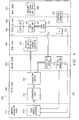
- FIGURE 6 illustrates a block diagram of exemplary next PC computation circuitry 500 according to one embodiment of the present invention.
- Next PC computation circuitry 500 illustratively includes an adder circuit 600, a counter circuit 605 and a multiplexor 610.
- Each of adder circuit 600 and counter circuit 605 receive the current program counter as an input.
- Adder circuit 600 also receives an offset value (for branching) as another input.
- Multiplexor 610 receives as inputs the outputs of each of adder circuit 600 and counter circuit 605, and operates to select one of the same as a function of a condition signal.
- next PC computation circuitry 500 computes next program counter addresses. Commonly this is accomplished using counter circuit 605 to simply determine the next program counter address.
- program counter and branch unit 315 is operable to compute both a branch address and a next program counter address, as above-described. It is clear that the branch address calculation, which requires performing an addition, can proceed in parallel with the condition computation in the non-branching cluster. Furthermore, the application of the condition to the calculation consists purely of setting up a multiplexor - inherently a fast operation.
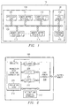
- FIGURE 7 illustrates a conceptual diagram of remote conditional branching control circuitry (generally designated 700) according to one embodiment of the present invention.
- Exemplary remote conditional branching control circuitry 700 illustratively includes a branching cluster 220 and a non-branching cluster 221.
- Exemplary branching cluster 220 illustratively includes program counter and branch unit 315 that illustratively includes next PC computation circuitry 500.
- Exemplary non-branching cluster 221 illustratively includes fetch stage 402, decode stage 403, register file 420 and execution stage 405; 406.
- FIGURE 8 illustrates a flow diagram (generally designated 800) of an exemplary method of operating data processor 100 when a conditional branch instruction is executing in a non-branching cluster according to one embodiment of the present invention.
- data processor 100 enters fetch stage 402 first, generating an instruction fetch address (process step 805; FADDR) and then enters decode stage 403 second.
- instruction buffer 305 of FIGURE 3 receives instructions as 128-bit wide words from instruction cache 215 and the instructions are dispatched to a cluster 220-222 of FIGURE 2 (process step 810).
- data processor 100 issues a shadow conditional branch instruction in branching cluster 220 causing program counter and branch unit 315 to perform a branch address computation as well as a next program counter address computation (process step 820), thereby enabling program counter and branch unit 315 via next PC computation circuitry 500 to evaluate branch instructions detected within the 128-bit wide words.
- Data processor 100 continues through the read stage where operands are generated by register file access, bypass and immediate (constant) generation block 420 (process step 825).
- the sources for operands are the register files, the constants (immediates) assembled from the instruction bundle, and any results bypassed from operations in later stages in the instruction pipeline.
- Data processor 100 continues through the instruction execution stage 405; 406, and non-branching cluster 221 executing the conditional branching instruction computes a branch condition and circuitry associating clusters 220-221 communicates the computed branch condition from non-branching cluster 221 to branching cluster 220 (Process step 830).
- a taken branch incurs a one cycle delay and the instruction being incorrectly fetched while the branch instruction is evaluated is discarded.
- conditional branch instructions require the calculation of a condition to decide whether the branch should be taken and a destination address.
- branch condition can be computed on any cluster 220-223 to eliminate movement of data between clusters.
- the computation of the destination address frequently consists of adding a constant to current program counter and does not require the ability to perform the calculation on an arbitrary cluster.
- a difficulty associated with implementing conditional branch instructions is their existence on critical instruction execution paths. This difficulty may suitably be reduced by performing the address calculation in parallel with the computation of the branch condition as above-described.
- branching cluster 220 via next PC computation circuitry 500 uses the computed branch condition to select one of the branch address or the next program counter address (process step 835).
- the exemplary branch architecture for a clustered machine illustrates several aspects of the principles hereof, namely, (i) early computation of the branch address minimizes taken branch penalties: if the branch address is computed late in the pipeline, cycles are lost before the instruction at the new address can be fetched B indicating that next PC address computation should be centralized in a single location; and (ii) issuance of compare operations on multiple clusters because working sets are distributed across the clusters, movement of all branch information to one specific cluster would unnecessarily increase inter-cluster traffic B B branching condition computation should be decentralized to the individual clusters.
Landscapes
- Engineering & Computer Science (AREA)
- Software Systems (AREA)
- Theoretical Computer Science (AREA)
- Physics & Mathematics (AREA)
- General Engineering & Computer Science (AREA)
- General Physics & Mathematics (AREA)
- Advance Control (AREA)
- Executing Machine-Instructions (AREA)
Abstract
Description
Claims (14)
- A data processor having a clustered architecture comprising:a branching cluster and a non-branching cluster, each capable of computing branch conditions, said branching cluster operable to perform branch address computations for said branching cluster and said non-branching cluster; andremote conditional branching control circuitry that causes said branching cluster to perform a branch address computation in response to sensing a conditional branch instruction in said non-branching cluster, and that communicates a computed branch condition from said non-branching cluster to said branching cluster.
- A processing system comprising:a data processor having a clustered architecture;a memory associated with said data processor;a plurality of peripheral circuits associated with said data processor for performing selected functions in association with said data processor, wherein said data processor comprises:at least a branching cluster and a non-branching cluster that are capable of computing branch conditions, said branching cluster operable to perform branch address computations for said at least said branching cluster and said non-branching cluster; andremote conditional branching control circuitry that causes said branching cluster to perform a branch address computation in response to sensing a conditional branch instruction in said non-branching cluster, and that communicates a computed branch condition from said non-branching cluster to said branching cluster.
- The processing system as set forth in Claim 2 or processor of Claim 1 wherein each of said branching cluster and said non-branching cluster comprises at least one register file.
- The processing system as set forth in Claim 2 or processor of Claim 1 wherein the or each of said branching cluster and said non-branching cluster comprises an instruction execution pipeline comprising N processing stages, each of said N processing stages capable of performing at least one of a plurality of execution steps associated with a pending instruction being executed by said instruction execution pipeline.
- The processing system as set forth in Claim 2 or processor of Claim 1 wherein said remote conditional branching control circuitry further causes said branching cluster to perform a next program counter address computation in response to sensing a conditional branch instruction in said non-branching cluster.
- The processing system or processor as set forth in Claim 5 wherein said remote conditional branching control circuitry selects one of said computed next program counter address and said computed branch address in response to said computed branch condition.
- The processing system as set forth in Claim 6 wherein said remote conditional branching control circuitry comprises a multiplexor responsive to said computed branch condition.
- The processing system as set forth in Claim 2 or the processor of Claim 1 wherein said data processor issues a shadow conditional branch instruction in said branching cluster to perform said branch address computation in response to sensing said conditional branch instruction in said non-branching cluster.
- For use in a data processor comprising at least a branching cluster and a non-branching cluster, each capable of computing branch conditions, said branching cluster operable to perform branch address computations for said branching cluster and said non-branching cluster, a method of operating said data processor comprising the steps of:computing a branch address in response to sensing a conditional branch instruction in said non-branching cluster; andcommunicating a branch condition computed by said non-branching cluster from said non-branching cluster to said branching cluster.
- The method of operating said data processor as set forth in Claim 9 further comprising the step of computing said branch condition in said non-branching cluster.
- The method of operating said data processor as set forth in Claim 10 further comprising the step of computing a next program counter address.
- The method of operating said data processor as set forth in Claim 11 further comprising the step of selecting one of said computed next program counter address and said computed branch address in response to said computed branch condition.
- The method of operating said data processor as set forth in Claim 9 wherein each of said branching cluster and said non-branching cluster comprises an instruction execution pipeline comprising N processing stages, said method further comprising the step of performing in each of said N processing stages at least one of a plurality of execution steps associated with a pending instruction being executed by said instruction execution pipeline.
- The method of operating said data processor as set forth in Claim 9 further comprising the step of issuing a shadow conditional branch instruction in said branching cluster to perform said branch address computation in response to sensing said conditional branch instruction in said non-branching cluster.
Applications Claiming Priority (2)
| Application Number | Priority Date | Filing Date | Title |
|---|---|---|---|
| US751410 | 1991-08-28 | ||
| US09/751,410 US7337306B2 (en) | 2000-12-29 | 2000-12-29 | Executing conditional branch instructions in a data processor having a clustered architecture |
Publications (3)
| Publication Number | Publication Date |
|---|---|
| EP1220089A2 true EP1220089A2 (en) | 2002-07-03 |
| EP1220089A3 EP1220089A3 (en) | 2002-11-13 |
| EP1220089B1 EP1220089B1 (en) | 2008-12-31 |
Family
ID=25021851
Family Applications (1)
| Application Number | Title | Priority Date | Filing Date |
|---|---|---|---|
| EP01310643A Expired - Lifetime EP1220089B1 (en) | 2000-12-29 | 2001-12-19 | Method for executing conditional branch instructions in a data processor and corresponding data processor |
Country Status (3)
| Country | Link |
|---|---|
| US (2) | US7337306B2 (en) |
| EP (1) | EP1220089B1 (en) |
| DE (1) | DE60137188D1 (en) |
Cited By (1)
| Publication number | Priority date | Publication date | Assignee | Title |
|---|---|---|---|---|
| CN103119537A (en) * | 2010-09-24 | 2013-05-22 | 英特尔公司 | Method and apparatus for reducing power consumption in a processor by powering down an instruction fetch unit |
Families Citing this family (9)
| Publication number | Priority date | Publication date | Assignee | Title |
|---|---|---|---|---|
| US6207646B1 (en) * | 1994-07-15 | 2001-03-27 | University Of Iowa Research Foundation | Immunostimulatory nucleic acid molecules |
| JP4368320B2 (en) * | 2005-03-16 | 2009-11-18 | 富士通株式会社 | Information processing system, pipeline processing apparatus, busy determination program, and computer-readable recording medium recording the program |
| US8370671B2 (en) * | 2009-12-02 | 2013-02-05 | International Business Machines Corporation | Saving power by powering down an instruction fetch array based on capacity history of instruction buffer |
| KR101140459B1 (en) * | 2010-09-15 | 2012-04-30 | 김형선 | Kitchenware with a detachable handle |
| WO2017014776A1 (en) * | 2015-07-22 | 2017-01-26 | Hewlett Packard Enterprise Development Lp | Startup circuit to initialize voltage reference circuit |
| JP6769106B2 (en) * | 2016-05-18 | 2020-10-14 | 富士通株式会社 | Storage control method, storage control program and information processing device |
| US10915324B2 (en) * | 2018-08-16 | 2021-02-09 | Tachyum Ltd. | System and method for creating and executing an instruction word for simultaneous execution of instruction operations |
| US11204768B2 (en) * | 2019-11-06 | 2021-12-21 | Onnivation Llc | Instruction length based parallel instruction demarcator |
| US20240281251A1 (en) * | 2019-11-06 | 2024-08-22 | Sitaram Yadavalli | Instruction length based parallel instruction demarcator |
Family Cites Families (7)
| Publication number | Priority date | Publication date | Assignee | Title |
|---|---|---|---|---|
| US4777589A (en) * | 1985-06-28 | 1988-10-11 | Hewlett-Packard Company | Direct input/output in a virtual memory system |
| US4991080A (en) * | 1986-03-13 | 1991-02-05 | International Business Machines Corporation | Pipeline processing apparatus for executing instructions in three streams, including branch stream pre-execution processor for pre-executing conditional branch instructions |
| US4833599A (en) * | 1987-04-20 | 1989-05-23 | Multiflow Computer, Inc. | Hierarchical priority branch handling for parallel execution in a parallel processor |
| CA2019299C (en) * | 1989-06-22 | 2002-01-15 | Steven Frank | Multiprocessor system with multiple instruction sources |
| DE69130519T2 (en) * | 1990-06-29 | 1999-06-10 | Digital Equipment Corp., Maynard, Mass. | High-performance multiprocessor with floating point unit and method for its operation |
| US5539888A (en) * | 1993-12-23 | 1996-07-23 | Unisys Corporation | System and method for processing external conditional branch instructions |
| US6772355B2 (en) * | 2000-12-29 | 2004-08-03 | Stmicroelectronics, Inc. | System and method for reducing power consumption in a data processor having a clustered architecture |
-
2000
- 2000-12-29 US US09/751,410 patent/US7337306B2/en not_active Expired - Lifetime
-
2001
- 2001-12-19 DE DE60137188T patent/DE60137188D1/en not_active Expired - Fee Related
- 2001-12-19 EP EP01310643A patent/EP1220089B1/en not_active Expired - Lifetime
-
2007
- 2007-09-14 US US11/900,978 patent/US7779240B2/en not_active Expired - Fee Related
Cited By (2)
| Publication number | Priority date | Publication date | Assignee | Title |
|---|---|---|---|---|
| CN103119537A (en) * | 2010-09-24 | 2013-05-22 | 英特尔公司 | Method and apparatus for reducing power consumption in a processor by powering down an instruction fetch unit |
| CN103119537B (en) * | 2010-09-24 | 2017-07-11 | 英特尔公司 | Method and apparatus for reducing the power consumption in processor by making the power down of instruction pickup unit |
Also Published As
| Publication number | Publication date |
|---|---|
| EP1220089A3 (en) | 2002-11-13 |
| US20080010443A1 (en) | 2008-01-10 |
| US7337306B2 (en) | 2008-02-26 |
| EP1220089B1 (en) | 2008-12-31 |
| US7779240B2 (en) | 2010-08-17 |
| DE60137188D1 (en) | 2009-02-12 |
| US20020087848A1 (en) | 2002-07-04 |
Similar Documents
| Publication | Publication Date | Title |
|---|---|---|
| US6772355B2 (en) | System and method for reducing power consumption in a data processor having a clustered architecture | |
| US7779240B2 (en) | System and method for reducing power consumption in a data processor having a clustered architecture | |
| KR100284789B1 (en) | Method and apparatus for selecting the next instruction in a superscalar or ultra-long instruction wordcomputer with N-branches | |
| JPH09311786A (en) | Data processing device | |
| WO2004021173A2 (en) | Apparatus and method for scheduling instruction execution in functional units with issue lock mechanism | |
| US20110283089A1 (en) | modularized micro processor design | |
| US20060174089A1 (en) | Method and apparatus for embedding wide instruction words in a fixed-length instruction set architecture | |
| US7143268B2 (en) | Circuit and method for instruction compression and dispersal in wide-issue processors | |
| EP1221648B1 (en) | Bypass circuitry for use in a pipelined processor | |
| EP1220092B1 (en) | System and method for executing variable latency load operations in a data processor | |
| EP1220100B1 (en) | Circuit and method for hardware-assisted software flushing of data and instruction caches | |
| EP1220088B1 (en) | Circuit and method for supporting misaligned accesses in the presence of speculative load instructions | |
| US7028164B2 (en) | Instruction fetch apparatus for wide issue processors and method of operation | |
| US6119220A (en) | Method of and apparatus for supplying multiple instruction strings whose addresses are discontinued by branch instructions | |
| US6865665B2 (en) | Processor pipeline cache miss apparatus and method for operation | |
| US6922773B2 (en) | System and method for encoding constant operands in a wide issue processor | |
| EP1235139B1 (en) | System and method for supporting precise exceptions in a data processor having a clustered architecture | |
| EP1050805B1 (en) | Transfer of guard values in a computer system | |
| JP2025185777A (en) | Vector operation processor and operation execution method for vector operation processor | |
| JP2861234B2 (en) | Instruction processing unit |
Legal Events
| Date | Code | Title | Description |
|---|---|---|---|
| PUAI | Public reference made under article 153(3) epc to a published international application that has entered the european phase |
Free format text: ORIGINAL CODE: 0009012 |
|
| AK | Designated contracting states |
Kind code of ref document: A2 Designated state(s): AT BE CH CY DE DK ES FI FR GB GR IE IT LI LU MC NL PT SE TR |
|
| AX | Request for extension of the european patent |
Free format text: AL;LT;LV;MK;RO;SI |
|
| PUAL | Search report despatched |
Free format text: ORIGINAL CODE: 0009013 |
|
| AK | Designated contracting states |
Kind code of ref document: A3 Designated state(s): AT BE CH CY DE DK ES FI FR GB GR IE IT LI LU MC NL PT SE TR |
|
| AX | Request for extension of the european patent |
Free format text: AL;LT;LV;MK;RO;SI |
|
| 17P | Request for examination filed |
Effective date: 20030509 |
|
| AKX | Designation fees paid |
Designated state(s): DE FR GB IT |
|
| 17Q | First examination report despatched |
Effective date: 20070730 |
|
| GRAP | Despatch of communication of intention to grant a patent |
Free format text: ORIGINAL CODE: EPIDOSNIGR1 |
|
| RTI1 | Title (correction) |
Free format text: METHOD FOR EXECUTING CONDITIONAL BRANCH INSTRUCTIONS IN A DATA PROCESSOR AND CORRESPONDING DATA PROCESSOR |
|
| GRAS | Grant fee paid |
Free format text: ORIGINAL CODE: EPIDOSNIGR3 |
|
| GRAA | (expected) grant |
Free format text: ORIGINAL CODE: 0009210 |
|
| AK | Designated contracting states |
Kind code of ref document: B1 Designated state(s): DE FR GB IT |
|
| REG | Reference to a national code |
Ref country code: GB Ref legal event code: FG4D |
|
| REF | Corresponds to: |
Ref document number: 60137188 Country of ref document: DE Date of ref document: 20090212 Kind code of ref document: P |
|
| PLBE | No opposition filed within time limit |
Free format text: ORIGINAL CODE: 0009261 |
|
| STAA | Information on the status of an ep patent application or granted ep patent |
Free format text: STATUS: NO OPPOSITION FILED WITHIN TIME LIMIT |
|
| 26N | No opposition filed |
Effective date: 20091001 |
|
| PG25 | Lapsed in a contracting state [announced via postgrant information from national office to epo] |
Ref country code: DE Free format text: LAPSE BECAUSE OF NON-PAYMENT OF DUE FEES Effective date: 20100701 |
|
| PG25 | Lapsed in a contracting state [announced via postgrant information from national office to epo] |
Ref country code: IT Free format text: LAPSE BECAUSE OF FAILURE TO SUBMIT A TRANSLATION OF THE DESCRIPTION OR TO PAY THE FEE WITHIN THE PRESCRIBED TIME-LIMIT Effective date: 20081231 |
|
| REG | Reference to a national code |
Ref country code: FR Ref legal event code: PLFP Year of fee payment: 15 |
|
| REG | Reference to a national code |
Ref country code: FR Ref legal event code: PLFP Year of fee payment: 16 |
|
| REG | Reference to a national code |
Ref country code: FR Ref legal event code: PLFP Year of fee payment: 17 |
|
| PGFP | Annual fee paid to national office [announced via postgrant information from national office to epo] |
Ref country code: GB Payment date: 20201123 Year of fee payment: 20 Ref country code: FR Payment date: 20201120 Year of fee payment: 20 |
|
| REG | Reference to a national code |
Ref country code: GB Ref legal event code: PE20 Expiry date: 20211218 |
|
| PG25 | Lapsed in a contracting state [announced via postgrant information from national office to epo] |
Ref country code: GB Free format text: LAPSE BECAUSE OF EXPIRATION OF PROTECTION Effective date: 20211218 |