EP1218934B1 - Method for determining the endpoint of etch process steps - Google Patents
Method for determining the endpoint of etch process steps Download PDFInfo
- Publication number
- EP1218934B1 EP1218934B1 EP00964248A EP00964248A EP1218934B1 EP 1218934 B1 EP1218934 B1 EP 1218934B1 EP 00964248 A EP00964248 A EP 00964248A EP 00964248 A EP00964248 A EP 00964248A EP 1218934 B1 EP1218934 B1 EP 1218934B1
- Authority
- EP
- European Patent Office
- Prior art keywords
- endpoint
- thickness
- wafer
- etch
- depth
- Prior art date
- Legal status (The legal status is an assumption and is not a legal conclusion. Google has not performed a legal analysis and makes no representation as to the accuracy of the status listed.)
- Expired - Lifetime
Links
Images
Classifications
-
- H—ELECTRICITY
- H10—SEMICONDUCTOR DEVICES; ELECTRIC SOLID-STATE DEVICES NOT OTHERWISE PROVIDED FOR
- H10P—GENERIC PROCESSES OR APPARATUS FOR THE MANUFACTURE OR TREATMENT OF DEVICES COVERED BY CLASS H10
- H10P74/00—Testing or measuring during manufacture or treatment of wafers, substrates or devices
-
- B—PERFORMING OPERATIONS; TRANSPORTING
- B24—GRINDING; POLISHING
- B24B—MACHINES, DEVICES, OR PROCESSES FOR GRINDING OR POLISHING; DRESSING OR CONDITIONING OF ABRADING SURFACES; FEEDING OF GRINDING, POLISHING, OR LAPPING AGENTS
- B24B37/00—Lapping machines or devices; Accessories
- B24B37/005—Control means for lapping machines or devices
- B24B37/013—Devices or means for detecting lapping completion
-
- H—ELECTRICITY
- H01—ELECTRIC ELEMENTS
- H01J—ELECTRIC DISCHARGE TUBES OR DISCHARGE LAMPS
- H01J37/00—Discharge tubes with provision for introducing objects or material to be exposed to the discharge, e.g. for the purpose of examination or processing thereof
- H01J37/32—Gas-filled discharge tubes
- H01J37/32917—Plasma diagnostics
- H01J37/32935—Monitoring and controlling tubes by information coming from the object and/or discharge
-
- H—ELECTRICITY
- H10—SEMICONDUCTOR DEVICES; ELECTRIC SOLID-STATE DEVICES NOT OTHERWISE PROVIDED FOR
- H10P—GENERIC PROCESSES OR APPARATUS FOR THE MANUFACTURE OR TREATMENT OF DEVICES COVERED BY CLASS H10
- H10P74/00—Testing or measuring during manufacture or treatment of wafers, substrates or devices
- H10P74/23—Testing or measuring during manufacture or treatment of wafers, substrates or devices characterised by multiple measurements, corrections, marking or sorting processes
- H10P74/238—Testing or measuring during manufacture or treatment of wafers, substrates or devices characterised by multiple measurements, corrections, marking or sorting processes comprising acting in response to an ongoing measurement without interruption of processing, e.g. endpoint detection or in-situ thickness measurement
Definitions
- the invention is directed to a method for determining the endpoint of etch process steps e.g. during recess etch steps of wafers by way of an optical endpoint determination system which is applied to a vacuum etch chamber within the etch steps are carried out.
- etch process steps such as the recess 2 and recess 3 steps are carried out within a vacuum chamber or a chamber with a low internal pressure.
- the vacuum chamber is normally provided with a plasma source for ionizing an etching gas which is introduced in the chamber.
- etching gas such as PAD nitride.
- an endpoint measuring system has improved achieving the target depths.
- the chamber is further provided with a dome to separate the vacuum chamber from the environment. For this measuring system this dome has a window for determining the endpoint of the etching process at its top end.
- Such an endpoint determining system is an optical system which monitors the etch process and incorporates an interferometric measuring system which determines the depth of the etched recesses or trenches in a semiconductor wafer positioned in the chamber on the top of a base.
- the target depths are referenced from the silicon surface which is usually below a masking layer (PAD nitride).
- PAD nitride a masking layer
- the problem is that the masking layer can vary from lot to lot or from wafer to wafer.
- the problem regarding the endpoint determination system is therefore that Interferometric Endpoint measuring systems (IEP) are able to determine the depth of a hole or a trench but the depth which is determined is not the target depth.
- the measured depth is depending from the thickness of the masking layer on the top surface of the silicon. Therefore the depth of e.g. recess 2 and recess 3 varies depending from the thickness of the masking layer.
- Another object of the present invention is to minimize the necessary tool adaption.
- a further object of the present invention is to provide a method which can be used on all etches which must stop in the film being etched and not at an interface.
- This new method eliminates the influences of different thickness of the masking layer and can be used on all etches which must stop in the film being etched and not at an interface. Also the necessary tool adaption is minimized.
- the measuring step is carried out with a laser measurement system which is based on ellipsometry.
- this step is carried out with the laser measuring system which is preferably directed to the centre of the wafer.
- the layer on top of the wafer is preferably a nitride layer, e. g. a PAD nitride layer.
- the new method is capable for 300 mm wafers and future embodiements.
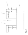
- Figure 1 illustrates schematically the depth of an etched hole 1 e.g. a trench with the target depth within a poly Si layer 2.
- This target depth is the ideal depth which is necessary to built up a functional element within the wafer 3.
- the mentioned Interferometric Endpoint measuring systems 6 are used. This IEP systems are able to determine the depth of a hole 1 or a trench but the depth that is determined is not the target depth. From Figure 1 it is to be seen that the determinable depth is a sum of the thickness x of the PAD nitride layer 4 and the target depth. If the thickness of the PAD nitride layer 4 is unknown then the measured depth at the endpoint is equal to the target depth and therefore the etched hole 1 or trench is not deep enough.
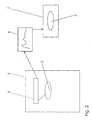
- This measuring step which is carried out by a laser measurement system 8 based on ellipsometry determines the thickness of the PAD nitride 4 on the top of the wafer 3 first and then the measurement (film thickness data) is forwarded to the endpoint determination system.
- the measurement is added to the target of the endpoint algorithm.
- the current etch step is stopped if the target depth plus the value of the measurement is reached.
- this step is carried out with the laser measuring system which is directed to the centre of the wafer 3.
- the new method provides a wafer to wafer endpoint target determination through PAD-nitride thickness measurement in parallel to wafer alignment which eliminates the influences of different thickness of the masking layer and can be used on all etches which must stop in the film beeing etched and not at an interface.
Landscapes
- Engineering & Computer Science (AREA)
- Physics & Mathematics (AREA)
- Plasma & Fusion (AREA)
- Chemical & Material Sciences (AREA)
- Analytical Chemistry (AREA)
- Mechanical Engineering (AREA)
- Length Measuring Devices By Optical Means (AREA)
- Testing Or Measuring Of Semiconductors Or The Like (AREA)
- Drying Of Semiconductors (AREA)
Abstract
Description
- The invention is directed to a method for determining the endpoint of etch process steps e.g. during recess etch steps of wafers by way of an optical endpoint determination system which is applied to a vacuum etch chamber within the etch steps are carried out.
- Several etch process steps such as the recess 2 and recess 3 steps are carried out within a vacuum chamber or a chamber with a low internal pressure. The vacuum chamber is normally provided with a plasma source for ionizing an etching gas which is introduced in the chamber. At front end of an etch step it is necessary to provide a wafer with an etch mask such as PAD nitride.
- Many product types incorporate process steps which require blind etches which stop within a film layer, such processes include Recess Etches and Shallow Trench Isolation. The use of an endpoint measuring system has improved achieving the target depths. The chamber is further provided with a dome to separate the vacuum chamber from the environment. For this measuring system this dome has a window for determining the endpoint of the etching process at its top end. Such an endpoint determining system is an optical system which monitors the etch process and incorporates an interferometric measuring system which determines the depth of the etched recesses or trenches in a semiconductor wafer positioned in the chamber on the top of a base.
- The target depths are referenced from the silicon surface which is usually below a masking layer (PAD nitride). The problem is that the masking layer can vary from lot to lot or from wafer to wafer. The problem regarding the endpoint determination system is therefore that Interferometric Endpoint measuring systems (IEP) are able to determine the depth of a hole or a trench but the depth which is determined is not the target depth. The measured depth is depending from the thickness of the masking layer on the top surface of the silicon. Therefore the depth of e.g. recess 2 and
recess 3 varies depending from the thickness of the masking layer. - For this reason a film measurement step is required to obtain the necessary offset required to setup the IEP. This number is either the measurement of one wafer or the average of several wafers. The current endpoint systems allow for ony one input per lot.
- In J. Vac. Sci and Technol. A, vol. 11, n°4, pages 1179-1185 is disclosed the use of ellipsometry to monitor etching in poly-buffered LOCOS process.
- It is an object of the present invention to provide a method for determining the endpoint of an etch process step during recess etch steps which eliminates the influence of different thickness of the masking layer.
- Another object of the present invention is to minimize the necessary tool adaption.
- A further object of the present invention is to provide a method which can be used on all etches which must stop in the film being etched and not at an interface.
- It is also an object of the invention to provide a method which is capable for 300 mm wafers and future embodiments.
- In accordance with one object of the invention there is provided a method for determining the endpoint of etch process steps as defined in claim 1.
- This new method eliminates the influences of different thickness of the masking layer and can be used on all etches which must stop in the film being etched and not at an interface.
Also the necessary tool adaption is minimized. - The measuring step is carried out with a laser measurement system which is based on ellipsometry.
- To minimize the time for the measuring step this step is carried out with the laser measuring system which is preferably directed to the centre of the wafer.
- The layer on top of the wafer is preferably a nitride layer, e. g. a PAD nitride layer.
- The new method is capable for 300 mm wafers and future embodiements.
-
- Fig. 1
- illustrates schematically the depth of an etched trench with the target depth and the IEP target; and
- Fig. 2
- illustrates schematically the new method for determining the endpoint of etch steps e.g. during recess etch steps of wafers.
- Figure 1 illustrates schematically the depth of an etched hole 1 e.g. a trench with the target depth within a poly Si layer 2. This target depth is the ideal depth which is necessary to built up a functional element within the
wafer 3. To determine the endpoint of an etch process the mentioned InterferometricEndpoint measuring systems 6 are used. This IEP systems are able to determine the depth of a hole 1 or a trench but the depth that is determined is not the target depth. From Figure 1 it is to be seen that the determinable depth is a sum of the thickness x of thePAD nitride layer 4 and the target depth. If the thickness of thePAD nitride layer 4 is unknown then the measured depth at the endpoint is equal to the target depth and therefore the etched hole 1 or trench is not deep enough. - According to Figure 2 there is introduced an additional step which is carried out in parallel to the
alignment stage 5 in the front end of the etch process 7. This additional step covers a thickness measuring step to determine the thickness of thePAD nitride 4 of eachwafer 3 introduced to the etch process 7. - This measuring step which is carried out by a
laser measurement system 8 based on ellipsometry determines the thickness of thePAD nitride 4 on the top of thewafer 3 first and then the measurement (film thickness data) is forwarded to the endpoint determination system. In this endpoint determination system (IEP) the measurement is added to the target of the endpoint algorithm. The current etch step is stopped if the target depth plus the value of the measurement is reached. - To minimize the time for the measuring step this step is carried out with the laser measuring system which is directed to the centre of the
wafer 3. - The new method provides a wafer to wafer endpoint target determination through PAD-nitride thickness measurement in parallel to wafer alignment which eliminates the influences of different thickness of the masking layer and can be used on all etches which must stop in the film beeing etched and not at an interface.
Claims (3)
- Method for determining the endpoint of an etch step during a recess etch of a semiconductor wafer having a mask layer on top of a substrate in a vacuum etch chamber, the method comprising the steps of:- performing a wafer alignment in the front end of the etch step;- measuring the thickness of the mask layer on top of the wafer using a laser measurement system, which performs ellipsometry, while performing the wafer alignment step to determine a thickness value representing the thickness of the mask layer;- forwarding the thickness value to an interferometric endpoint determination system performing an endpoint algorithm;- adding the thickness value to a target depth value of the endpoint algorithm;- etching a recess into the substrate relative to a mask provided by the mask layer;- measuring the depth of the recess during the etch step to obtain a depth value representing the depth of the recess;- wherein the etch step is stopped when the depth value reaches the sum of the target depth value and the thickness value.
- Method according to claim 1, characterized in that the step of measuring the thickness is carried out with the laser measuring system which is directed to the centre of the wafer.
- Method according to any of claims 1 to 2, characterized in that the mask layer is a nitride (4) layer.
Priority Applications (1)
| Application Number | Priority Date | Filing Date | Title |
|---|---|---|---|
| EP00964248A EP1218934B1 (en) | 1999-09-30 | 2000-09-28 | Method for determining the endpoint of etch process steps |
Applications Claiming Priority (4)
| Application Number | Priority Date | Filing Date | Title |
|---|---|---|---|
| EP99119443 | 1999-09-30 | ||
| EP99119443A EP1089318A1 (en) | 1999-09-30 | 1999-09-30 | Method for determining the endpoint of etch process steps |
| EP00964248A EP1218934B1 (en) | 1999-09-30 | 2000-09-28 | Method for determining the endpoint of etch process steps |
| PCT/EP2000/009518 WO2001024254A1 (en) | 1999-09-30 | 2000-09-28 | Method for determining the endpoint of etch process steps |
Publications (2)
| Publication Number | Publication Date |
|---|---|
| EP1218934A1 EP1218934A1 (en) | 2002-07-03 |
| EP1218934B1 true EP1218934B1 (en) | 2006-12-20 |
Family
ID=8239097
Family Applications (2)
| Application Number | Title | Priority Date | Filing Date |
|---|---|---|---|
| EP99119443A Withdrawn EP1089318A1 (en) | 1999-09-30 | 1999-09-30 | Method for determining the endpoint of etch process steps |
| EP00964248A Expired - Lifetime EP1218934B1 (en) | 1999-09-30 | 2000-09-28 | Method for determining the endpoint of etch process steps |
Family Applications Before (1)
| Application Number | Title | Priority Date | Filing Date |
|---|---|---|---|
| EP99119443A Withdrawn EP1089318A1 (en) | 1999-09-30 | 1999-09-30 | Method for determining the endpoint of etch process steps |
Country Status (8)
| Country | Link |
|---|---|
| US (1) | US20030010750A1 (en) |
| EP (2) | EP1089318A1 (en) |
| JP (1) | JP2003510844A (en) |
| KR (1) | KR100474174B1 (en) |
| DE (1) | DE60032498T2 (en) |
| IL (1) | IL148750A (en) |
| TW (1) | TW573334B (en) |
| WO (1) | WO2001024254A1 (en) |
Families Citing this family (6)
| Publication number | Priority date | Publication date | Assignee | Title |
|---|---|---|---|---|
| TW472336B (en) * | 2001-02-21 | 2002-01-11 | Promos Technologies Inc | Method for controlling etching depth |
| US6728591B1 (en) * | 2001-08-01 | 2004-04-27 | Advanced Micro Devices, Inc. | Method and apparatus for run-to-run control of trench profiles |
| US8257546B2 (en) * | 2003-04-11 | 2012-09-04 | Applied Materials, Inc. | Method and system for monitoring an etch process |
| KR101093914B1 (en) | 2003-11-28 | 2011-12-13 | 코닝 인코포레이티드 | Manufacturing Method of Glass Panel |
| US7279657B2 (en) * | 2005-06-13 | 2007-10-09 | Applied Materials, Inc. | Scanned rapid thermal processing with feed forward control |
| US7521332B2 (en) * | 2007-03-23 | 2009-04-21 | Alpha & Omega Semiconductor, Ltd | Resistance-based etch depth determination for SGT technology |
Family Cites Families (7)
| Publication number | Priority date | Publication date | Assignee | Title |
|---|---|---|---|---|
| US4680084A (en) * | 1984-08-21 | 1987-07-14 | American Telephone And Telegraph Company, At&T Bell Laboratories | Interferometric methods and apparatus for device fabrication |
| FR2616269B1 (en) * | 1987-06-04 | 1990-11-09 | Labo Electronique Physique | TEST DEVICE FOR IMPLEMENTING A PROCESS FOR PRODUCING SEMICONDUCTOR DEVICES |
| US5362356A (en) * | 1990-12-20 | 1994-11-08 | Lsi Logic Corporation | Plasma etching process control |
| US5407524A (en) * | 1993-08-13 | 1995-04-18 | Lsi Logic Corporation | End-point detection in plasma etching by monitoring radio frequency matching network |
| US5465859A (en) * | 1994-04-28 | 1995-11-14 | International Business Machines Corporation | Dual phase and hybrid phase shifting mask fabrication using a surface etch monitoring technique |
| US5877407A (en) * | 1997-07-22 | 1999-03-02 | Lucent Technologies Inc. | Plasma etch end point detection process |
| US6136712A (en) * | 1998-09-30 | 2000-10-24 | Lam Research Corporation | Method and apparatus for improving accuracy of plasma etching process |
-
1999
- 1999-09-30 EP EP99119443A patent/EP1089318A1/en not_active Withdrawn
-
2000
- 2000-09-28 JP JP2001527345A patent/JP2003510844A/en active Pending
- 2000-09-28 WO PCT/EP2000/009518 patent/WO2001024254A1/en not_active Ceased
- 2000-09-28 IL IL14875000A patent/IL148750A/en not_active IP Right Cessation
- 2000-09-28 EP EP00964248A patent/EP1218934B1/en not_active Expired - Lifetime
- 2000-09-28 DE DE60032498T patent/DE60032498T2/en not_active Expired - Fee Related
- 2000-09-28 KR KR10-2002-7004114A patent/KR100474174B1/en not_active Expired - Fee Related
- 2000-09-29 TW TW89120230A patent/TW573334B/en not_active IP Right Cessation
-
2002
- 2002-04-01 US US10/113,344 patent/US20030010750A1/en not_active Abandoned
Also Published As
| Publication number | Publication date |
|---|---|
| EP1089318A1 (en) | 2001-04-04 |
| DE60032498D1 (en) | 2007-02-01 |
| EP1218934A1 (en) | 2002-07-03 |
| JP2003510844A (en) | 2003-03-18 |
| KR100474174B1 (en) | 2005-03-10 |
| IL148750A (en) | 2005-11-20 |
| US20030010750A1 (en) | 2003-01-16 |
| KR20020085879A (en) | 2002-11-16 |
| TW573334B (en) | 2004-01-21 |
| WO2001024254A1 (en) | 2001-04-05 |
| DE60032498T2 (en) | 2007-10-04 |
| IL148750A0 (en) | 2002-09-12 |
Similar Documents
| Publication | Publication Date | Title |
|---|---|---|
| KR100852372B1 (en) | Integrated shallow trench isolation approach | |
| US6391788B1 (en) | Two etchant etch method | |
| EP0743674B1 (en) | Method of etching back layer on substrate | |
| KR100659163B1 (en) | Method and apparatus for improving the accuracy of the plasma etching process | |
| US6939811B2 (en) | Apparatus and method for controlling etch depth | |
| US6919259B2 (en) | Method for STI etching using endpoint detection | |
| GB2393852A (en) | Method and apparatus for controlling etch selectivity | |
| MY113155A (en) | Method of manufacturing semiconductor wafers | |
| WO2002069383A3 (en) | Method of forming a notched silicon-containing gate structure | |
| US7964473B2 (en) | Method of filling an opening in the manufacturing of a semiconductor device | |
| EP1089318A1 (en) | Method for determining the endpoint of etch process steps | |
| US20040038541A1 (en) | Method for etching a hard mask layer and a metal layer | |
| US7425510B2 (en) | Methods of cleaning processing chamber in semiconductor device fabrication equipment | |
| US7204934B1 (en) | Method for planarization etch with in-situ monitoring by interferometry prior to recess etch | |
| US6333271B1 (en) | Multi-step plasma etch method for plasma etch processing a microelectronic layer | |
| US7087498B2 (en) | Method for controlling trench depth in shallow trench isolation features | |
| US5261998A (en) | Method for detecting an end point of etching in semiconductor manufacture using the emission spectrum of helium | |
| JPH1064886A (en) | Dry etching apparatus and dry etching method | |
| US6806200B2 (en) | Method of improving etch uniformity in deep silicon etching | |
| US6500725B1 (en) | Microelectronic fabrication method providing alignment mark and isolation trench of identical depth | |
| JPH0334426A (en) | Forming method of buried oxide film | |
| EP0961315A1 (en) | Chemical mechanical polishing process for integrated circuits using a patterned stop layer | |
| KR20020010295A (en) | Method for detecting end-point of chemical mechanical polishing | |
| JPH06104215A (en) | Method for manufacturing semiconductor device | |
| KR20040038141A (en) | Method for detecting polishing end point in chemical mechanical polishing process |
Legal Events
| Date | Code | Title | Description |
|---|---|---|---|
| PUAI | Public reference made under article 153(3) epc to a published international application that has entered the european phase |
Free format text: ORIGINAL CODE: 0009012 |
|
| 17P | Request for examination filed |
Effective date: 20020315 |
|
| AK | Designated contracting states |
Kind code of ref document: A1 Designated state(s): AT BE CH CY DE DK ES FI FR GB GR IE IT LI LU MC NL PT SE |
|
| RBV | Designated contracting states (corrected) |
Designated state(s): AT DE |
|
| GRAP | Despatch of communication of intention to grant a patent |
Free format text: ORIGINAL CODE: EPIDOSNIGR1 |
|
| GRAS | Grant fee paid |
Free format text: ORIGINAL CODE: EPIDOSNIGR3 |
|
| GRAA | (expected) grant |
Free format text: ORIGINAL CODE: 0009210 |
|
| RAP1 | Party data changed (applicant data changed or rights of an application transferred) |
Owner name: MOTOROLA, INC. Owner name: QIMONDA AG Owner name: QIMONDA DRESDEN GMBH & CO. OHG |
|
| RBV | Designated contracting states (corrected) |
Designated state(s): DE |
|
| AK | Designated contracting states |
Kind code of ref document: B1 Designated state(s): DE |
|
| REF | Corresponds to: |
Ref document number: 60032498 Country of ref document: DE Date of ref document: 20070201 Kind code of ref document: P |
|
| PLBE | No opposition filed within time limit |
Free format text: ORIGINAL CODE: 0009261 |
|
| STAA | Information on the status of an ep patent application or granted ep patent |
Free format text: STATUS: NO OPPOSITION FILED WITHIN TIME LIMIT |
|
| 26N | No opposition filed |
Effective date: 20070921 |
|
| PGFP | Annual fee paid to national office [announced via postgrant information from national office to epo] |
Ref country code: DE Payment date: 20071113 Year of fee payment: 8 |
|
| PG25 | Lapsed in a contracting state [announced via postgrant information from national office to epo] |
Ref country code: DE Free format text: LAPSE BECAUSE OF NON-PAYMENT OF DUE FEES Effective date: 20090401 |