EP1217863A2 - Unified associative memory of data channel schedulers in an optical router - Google Patents
Unified associative memory of data channel schedulers in an optical router Download PDFInfo
- Publication number
- EP1217863A2 EP1217863A2 EP01129348A EP01129348A EP1217863A2 EP 1217863 A2 EP1217863 A2 EP 1217863A2 EP 01129348 A EP01129348 A EP 01129348A EP 01129348 A EP01129348 A EP 01129348A EP 1217863 A2 EP1217863 A2 EP 1217863A2
- Authority
- EP
- European Patent Office
- Prior art keywords
- channels
- channel
- time
- optical
- outgoing
- Prior art date
- Legal status (The legal status is an assumption and is not a legal conclusion. Google has not performed a legal analysis and makes no representation as to the accuracy of the status listed.)
- Withdrawn
Links
- 230000003287 optical effect Effects 0.000 title claims abstract description 95
- 230000015654 memory Effects 0.000 title claims abstract description 52
- 230000001934 delay Effects 0.000 claims abstract description 8
- 239000013307 optical fiber Substances 0.000 claims abstract description 7
- 230000005540 biological transmission Effects 0.000 claims description 52
- 238000000034 method Methods 0.000 claims description 51
- 239000000872 buffer Substances 0.000 claims description 42
- 239000000835 fiber Substances 0.000 abstract description 8
- 238000010586 diagram Methods 0.000 description 28
- 102000029828 Melanin-concentrating hormone receptor Human genes 0.000 description 16
- 108010047068 Melanin-concentrating hormone receptor Proteins 0.000 description 16
- 238000013461 design Methods 0.000 description 12
- 230000008569 process Effects 0.000 description 8
- 230000003111 delayed effect Effects 0.000 description 7
- 238000005516 engineering process Methods 0.000 description 6
- 239000011159 matrix material Substances 0.000 description 6
- 101000741965 Homo sapiens Inactive tyrosine-protein kinase PRAG1 Proteins 0.000 description 5
- 102100038659 Inactive tyrosine-protein kinase PRAG1 Human genes 0.000 description 5
- 230000006870 function Effects 0.000 description 5
- 238000012986 modification Methods 0.000 description 5
- 230000004048 modification Effects 0.000 description 5
- 239000011800 void material Substances 0.000 description 4
- 238000013459 approach Methods 0.000 description 3
- 230000008901 benefit Effects 0.000 description 3
- 230000000903 blocking effect Effects 0.000 description 3
- 238000003491 array Methods 0.000 description 2
- 238000006243 chemical reaction Methods 0.000 description 2
- 239000013256 coordination polymer Substances 0.000 description 2
- 239000004744 fabric Substances 0.000 description 2
- 238000005192 partition Methods 0.000 description 2
- 230000004044 response Effects 0.000 description 2
- 238000004088 simulation Methods 0.000 description 2
- 230000004308 accommodation Effects 0.000 description 1
- 230000001174 ascending effect Effects 0.000 description 1
- 238000004891 communication Methods 0.000 description 1
- 230000003247 decreasing effect Effects 0.000 description 1
- 238000001514 detection method Methods 0.000 description 1
- 238000011161 development Methods 0.000 description 1
- 238000004519 manufacturing process Methods 0.000 description 1
- 238000013507 mapping Methods 0.000 description 1
- 230000006855 networking Effects 0.000 description 1
- 238000012545 processing Methods 0.000 description 1
- 230000003134 recirculating effect Effects 0.000 description 1
- 238000000638 solvent extraction Methods 0.000 description 1
- 238000012360 testing method Methods 0.000 description 1
- 230000001960 triggered effect Effects 0.000 description 1
Images






Classifications
-
- H—ELECTRICITY
- H04—ELECTRIC COMMUNICATION TECHNIQUE
- H04Q—SELECTING
- H04Q11/00—Selecting arrangements for multiplex systems
- H04Q11/0001—Selecting arrangements for multiplex systems using optical switching
- H04Q11/0005—Switch and router aspects
-
- H—ELECTRICITY
- H04—ELECTRIC COMMUNICATION TECHNIQUE
- H04Q—SELECTING
- H04Q11/00—Selecting arrangements for multiplex systems
- H04Q11/0001—Selecting arrangements for multiplex systems using optical switching
- H04Q11/0062—Network aspects
- H04Q11/0066—Provisions for optical burst or packet networks
-
- H—ELECTRICITY
- H04—ELECTRIC COMMUNICATION TECHNIQUE
- H04Q—SELECTING
- H04Q11/00—Selecting arrangements for multiplex systems
- H04Q11/0001—Selecting arrangements for multiplex systems using optical switching
- H04Q11/0005—Switch and router aspects
- H04Q2011/0007—Construction
- H04Q2011/002—Construction using optical delay lines or optical buffers or optical recirculation
-
- H—ELECTRICITY
- H04—ELECTRIC COMMUNICATION TECHNIQUE
- H04Q—SELECTING
- H04Q11/00—Selecting arrangements for multiplex systems
- H04Q11/0001—Selecting arrangements for multiplex systems using optical switching
- H04Q11/0062—Network aspects
- H04Q2011/0064—Arbitration, scheduling or medium access control aspects
-
- H—ELECTRICITY
- H04—ELECTRIC COMMUNICATION TECHNIQUE
- H04Q—SELECTING
- H04Q11/00—Selecting arrangements for multiplex systems
- H04Q11/0001—Selecting arrangements for multiplex systems using optical switching
- H04Q11/0062—Network aspects
- H04Q2011/0069—Network aspects using dedicated optical channels
Definitions
- This invention relates in general to telecommunications and, more particularly, to a method and apparatus for optical switching.
- the increase in Internet traffic requires a network with high capacity routers capable of routing data packets of variable length.
- One option is the use of optical networks.
- DWDM dense-wavelength division multiplexing
- optical burst-switched networking attempts to make the best use of optical and electronic switching technologies.
- the electronics provides dynamic control of system resources by assigning individual user data bursts to channels of a DWDM fiber, while optical technology is used to switch the user data channels entirely in the optical domain.
- an optical burst-switched router comprises an optical switch for routing optical information from an incoming optical transmission medium to one of a plurality of outgoing optical transmission media, each outgoing media able to transmit optical information over a plurality of channels.
- a delay buffer is coupled to the optical switch for providing a plurality of different delays for delaying selected information between the incoming transmission medium and one of the outgoing optical transmission media.
- Scheduling circuitry is associated with each respective outgoing medium, comprising an associative processor for storing information on both unscheduled time for each channel and time gaps on each channel on the respective outgoing medium.
- the present invention provides an efficient architecture for identifying unscheduled time and time gaps within which a data burst can be scheduled.
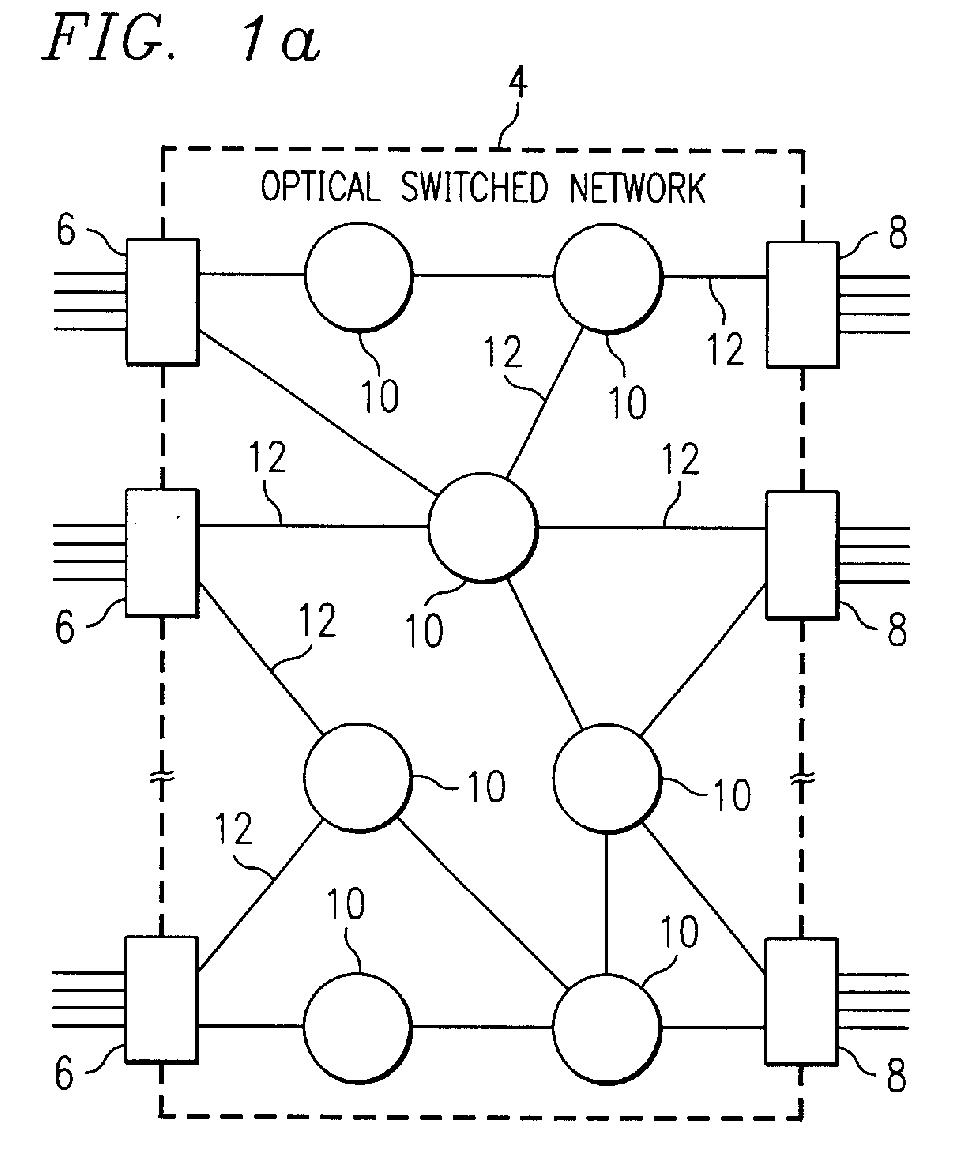
- FIG 1a illustrates a general block diagram of an optical burst switched network 4.
- the optical burst switched (OBS) network 4 includes multiple electronic ingress edge routers 6 and multiple egress edge routers 8.
- the ingress edge routers 6 and egress edge routers 8 are coupled to multiple core optical routers 10.
- the connections between ingress edge routers 6, egress edge routers 8 and core routers 10 are made using optical links 12.
- Each optical fiber can carry multiple channels of optical data.
- a data burst (or simply "burst") of optical data is the basic data block to be transferred through the network 4.
- Ingress edge routers 6 and egress edge routers 8 are responsible for burst assembly and disassembly functions, and serve as legacy interfaces between the optical burst switched network 4 and conventional electronic routers.
- the basic data block to be transferred is a burst, which is a collection of packets having some common attributes.
- a burst consists of a burst payload (called “data burst”) and a burst header (called “burst header packet” or BHP).
- data burst a burst payload
- burst header packet a burst header packet
- An intrinsic feature of the optical burst switched network is that a data burst and its BHP are transmitted on different channels and switched in optical and electronic domains, respectively, at each network node.
- the BHP is sent ahead of its associated data burst with an offset time ⁇ ( ⁇ 0). Its initial value, ⁇ 0 , is set by the (electronic) ingress edge router 8.
- a "channel” is defined as a certain unidirectional transmission capacity (in bits per second) between two adjacent routers.
- a channel may consist of one wavelength or a portion of a wavelength (e.g., when time-division multiplexing is used).
- Channels carrying data bursts are called “data channels”, and channels carrying BHPs and other control packets are called “control channels”.
- a "channel group” is a set of channels with a common type and node adjacency.
- a link is defined as a total transmission capacity between two routers, which usually consists of a "data channel group” (DCG) and a “control channel group” (CCG) in each direction.
- DCG data channel group
- CCG control channel group
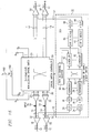
- FIG. 1b illustrates a block diagram of a core optical router 10.
- the incoming DCG 14 is separated from the CCG 16 for each fiber 12 by demultiplexer 18.
- Each DCG 14 is delayed by a fiber delay line (FDL) 19.
- the delayed DCG is separated into channels 20 by demultiplexer 22.
- Each channel 20 is input to a respective input node on a non-blocking spatial switch 24.
- Additional input and output nodes of spatial switch 24 are coupled to a recirculation buffer (RB) 26.
- Recirculation buffer 26 is controlled by a recirculation switch controller 28.
- Spatial switch 24 is controlled by a spatial switch controller 30.
- CCGs 14 are coupled to a switch control unit (SCU) 32.
- SCU includes an optical/electronic transceiver 34 for each CCG 14.
- the optical/electronic transceiver 34 receives the optical CCG control information and converts the optical information into electronic signals.
- the electronic CCG information is received by a packet processor 36, which passes information to a forwarder 38.
- the forwarder for each CCG is coupled to a switch 40.
- the output nodes of switch 40 are coupled to respective schedulers 42.
- Schedulers 42 are coupled to a Path & Channel Selector 44 and to respective BHP transmit modules 46.
- the BHP transmit modules 46 are coupled to electronic/optical transceivers 48.
- the electronic/optical transceivers produce the output CCG 52 to be combined with the respective output DCG 54 information by multiplexer 50.
- Path & channel selector 44 is also coupled to RB switch controller 28 and spatial switch controller 30.
- a DCG-CCG pair 52 is carried in one fiber.
- the optical router could be asymmetric, the number of channels k of a CCG 16 could be larger than one, and a DCG-CCG pair 52 could be carried in more than one fiber 12.
- BCG buffer channel group
- the optical switching matrix consists of a ( NK+R ) x ( NK+R ) spatial switch and a RxR switch with WDM (wavelength division multiplexing) FDL buffer serving as recirculation buffer (RB) 26 to resolve data burst contentions on outgoing data channels.
- the spatial switch is a strictly non-blocking switch, meaning that an arriving data burst on an incoming data channel can be switched to any idle outgoing data channel.
- the delay ⁇ introduced by the input FDL 19 should be sufficiently long such that the SCU 32 has enough time to process a BHP before its associated data burst enters the spatial switch.
- a data burst entering the RB switch on any incoming channel can be delayed by one of B delay times provided.
- the recirculation buffer in Figure 1b can be degenerated to passive FDL loops by removing the function of RB switch, as shown in Figure 15, wherein different buffer channels may have different delays.
- the SCU is partially based on an electronic router.
- the SCU has N input control channels and N output control channels.
- the SCU mainly consists of packet processors (PPs) 36, forwarders 38, a switching fabric 40, schedulers 42, BHP transmission modules 46, a path & channel selector 44, a spatial switch controller 30, and a RB switch controller 28.
- the packet processor 36, the forwarders 38, and the switching fabric 40 can be found in electronic routers.
- the other components, especially the scheduler, are new to optical routers.
- the design of the SCU uses the distributed control as much as possible, except the control to the access of shared FDL buffer which is centralized.
- the packet processor performs layer 1 and layer 2 decapsulation functions and attaches a time-stamp to each arriving BHP, which records the arrival time of the associated data burst to the OSM.
- the time-stamp is the sum of the BHP arrival time, the burst offset-time ⁇ carried by the BHP and the delay ⁇ introduced by input FDL 19.
- the forwarder mainly performs the forwarding table lookup to decide which outgoing CCG 52 to forward the BHP.
- the associated data burst will be switched to the corresponding DCG 54.
- the forwarding can be done in a connectionless or connection-oriented manner.
- the scheduler 42 schedules the switching of the data burst on a data channel of the outgoing DCG 54 based on the information carried by the BHP. If a free data channel is found, the scheduler 42 will then schedule the transmission of the BHP on the outgoing control channel, trying to "resynchronize" the BHP and its associated data burst by keeping the offset time ⁇ ( ⁇ 0) as close as possible to ⁇ 0 . After both the data burst and BHP are successfully scheduled, the scheduler 42 will send the configuration information to the spatial switch controller 30 if it is not necessary to provide a delay through the recirculation buffer 26, otherwise it will also send the configuration information to the RB switch controller 28.
- the scheduler 42 determines whether or not there is enough time to schedule an incoming data burst. If so, the scheduler determines whether the data burst can be scheduled, i.e., whether there is an unoccupied space in the specified output DCG 54 for the data burst. In order to schedule the data burst, there must be an available space to accommodate the data burst in the specified output DCG. This space may start within a time window beginning at the point of arrival of the data burst at the spatial switch 24 extending to the maximum delay which can be provided by the recirculation buffer 26. If the data burst can be scheduled, then the scheduler 42 must determine whether there is a space available in the output CCG 52 for the BHP in decision block 64.
- the configuration information from scheduler to path & channel selector includes incoming DCG identifier, incoming data channel identifier, outgoing DCG identifier, outgoing data channel identifier, data burst arrival time to the spatial switch, data burst duration, FDL identifier i ( Q i delay time is requested, 0 ⁇ i ⁇ B ).
- the path & channel selector 44 will simply forward the configuration information to the spatial switch controller 30. Otherwise, the path & channel selector 44 searches for an idle incoming buffer channel to the RB switch 26 in decision block 68. If found, the path and channel selector 44 searches for an idle outgoing buffer channel from the RB switch 26 to carry the data burst reentering the spatial switch after the specified delay inside the RB switch 26 in decision block 70. It is assumed that once the data burst enters the RB switch, it can be delayed for any discrete time from the set ⁇ Q 1 , Q 2 , ..., Q B ⁇ .
- the path & channel selector 44 will have to take the RB switch architecture into account. If both idle channels to and from the RB switch 26 are found, the path & channel selector 44 will send configuration information to the spatial switch controller 30 and the RB switch controller 28 and send an ACK (acknowledgement) back to the 42 scheduler. Otherwise, it will send a NACK (negative acknowledgement) back to the scheduler 42 and the BHP and data burst will be discarded in block 65.
- Configuration information from the path & channel selector 44 to the spatial switch controller 30 includes incoming DCG identifier, incoming data channel identifier, outgoing DCG identifier, outgoing data channel identifier, data burst arrival time to the spatial switch, data burst duration, FDL identifier i ( Q i delay time is requested, 0 ⁇ i ⁇ B ). If i > 0, the information also includes the incoming BCG identifier (to the RB switch), incoming buffer channel identifier (to the RB switch), outgoing BCG identifier (from the RB switch), and outgoing buffer channel identifier (from the RB switch).
- Configuration information from path & channel selector to RB switch controller includes an incoming BCG identifier (to the RB switch), incoming buffer channel identifier (to the RB switch), outgoing BCG identifier (from the RB switch), outgoing buffer channel identifier (from the RB switch), data burst arrival time to the RB switch, data burst duration, FDL identifier i ( Q i delay time is requested, 1 ⁇ i ⁇ B ).
- the spatial switch controller 30 and the RB switch controller 28 will perform the mapping from the configuration information received to physical components that involved in setting up the internal path(s), and configure the switches just-in-time to let the data burst fly-through the optical router 10.
- the spatial switch controller will set up two internal paths in the spatial switch, one from the incoming data channel to the incoming recirculation buffer channel when the data burst arrives to the spatial switch, another from the outgoing buffer channel to the outgoing data channel when the data burst reenters the spatial switch.
- the scheduler 42 Upon receiving the ACK from the path & channel selector 44, the scheduler 42 will update the state information of selected data and control channels, and is ready to process a new BHP.
- the BHP transmission module arranges the transmission of BHPs at times specified by the scheduler.
- FIG. 3 illustrates a block diagram of a scheduler 42.
- the scheduler 42 includes a scheduling queue 80, a BHP processor 82, a data channel scheduling (DCS) module 84, and a control channel scheduling (CCS) module 86.
- Each scheduler needs only to keep track of the busy/idle periods of its associated outgoing DCG 54 and outgoing CCG 52.
- BHPs arriving from the electronic switch are first stored in the scheduling queue 80. For basic operations, all that is required is one scheduling queue 80, however, virtual scheduling queues 80 may be maintained for different service classes. Each queue 80 could be served according to the arrival order of BHPs or according to the actual arrival order of their associated data bursts.
- the BHP processor 82 coordinates the data and control channel scheduling process and sends the configuration to the path & channel selector 44. It could trigger the DCS module 84 and the CCS module 82 in sequence or in parallel, depending on how the DCS and CCS modules 84 and 82 are implemented.
- the BHP processor 82 first triggers the DCS module 84 for scheduling the data burst (DB) on a data channel in a desired output DCS 54. After determining when the data burst will be sent out, the BHP processor then triggers the CCS module 86 for scheduling the BHP on an associated control channel.
- DB data burst
- the BHP processor then triggers the CCS module 86 for scheduling the BHP on an associated control channel.
- the BHP processor 82 triggers the DCS module 84 and CCS module 86 simultaneously. Since the CCS module 86 does not know when the data burst will be sent out, it schedules the BHP for all possible departure times of the data burst or its subset. There are in total B +1 possible departure times. Based on the actual data burst departure time reported from the DCS module 84, the BHP processor 86 will pick the right time to send out the BHP.
- T s be the duration (e.g., in ⁇ s) of a time slot in data channels and T f be the duration of a time slot in control channels.
- T s ⁇ r d Kbits of information can be sent during a slot if the data channel speed is r d gigabits per second.
- T f ⁇ r c Kbits of information can be sent during a slot if the control channel speed is r c gigabits per second.
- T f is equal to multiples of T s .
- time frame to designate time slot in control channels.
- (1) data bursts are variable length, in multiple of slots, which can only arrive at slot boundaries, and (2) BHPs are also variable length, in, for instance, multiple of bytes.
- the OSM is configured periodically.
- a typical example of the configuration period is one slot, although the configuration period could also be a multiple of slots.
- the length of a FDL Q i needs also to be a multiple of slots, 1 ⁇ i ⁇ B. Due to the slotted transmission and switching, it is suggested to use the time slot as a basic time unit in the SCU for the purpose of data channel scheduling, control channel scheduling and buffer channel scheduling, as well as synchronization between BHPs and their associated data bursts. This will simplify the design of various schedulers.
- Each arriving BHP to the SCU is time-stamped at the transceiver interface, right after O/E conversion, recording the beginning of the time frame during which the BHP enters the SCU.
- the most important variable is t DB , the DB arrival time to the OSM.
- t DB ( t BHP ⁇ T f + ⁇ + ⁇ ) mod 2 b .
- Timestamp t DB will be carried by the BHP within the SCU 32.
- ⁇ 100 slots
- 1 ⁇ ⁇ ⁇ ⁇ 0 8. It is assumed without loss of generality that the switching latency of the spatial switch in Figure 1b is negligible.
- the data burst arrival time t DB to the spatial switch 24 is also its departure time if no FDL buffer is used. Note that even if the switching latency is not negligible, t DB can still be used as the data burst departure time in channel scheduling as the switching latency is compensated at router output ports where data and control channels are resynchronized.
- FIG. 5 illustrates a block diagram of a DCS module 84.
- associative processor arrays P M 90 and P G 92 perform parallel searches of unscheduled channel times and gaps between scheduled channel times and update state information. Gaps and unscheduled times are represented in relative times.
- P M 90 and P G 92 are coupled to control processor CP 1 94.
- a LAUC-VF (Latest Available Unused Channel with Void Filling) scheduling principle is used to determine a desired scheduling, as described in connection with U.S. Ser. No. 09/689,584, entitled "Hardware Implementation of Channel Scheduling Algorithms of Optical Routers with FDL Buffers" to Zheng et al, filed October 12, 2000, and which is incorporated by reference herein.
- the DCS module 84 uses two b- bit slot counters, C and C 1 .
- Counter C keeps track of the time slots, which can be shared with the CCS module 86.
- Counter C 1 records the elapsed time slots since the last BHP is received. Both counters are incremented by every pulse of the slot clock. However, counter C 1 is reset to 0 when the DCS module 84 receives a new BHP. Once counter C 1 reaches 2 b -1, it stops counting, indicating that at least 2 b -1 slots have elapsed since the last BHP.
- the value of b should satisfy 2 b ⁇ W s where W s is the data channel scheduling window.
- Associative processor P M in Figure 5 is used to store the unscheduled time of each data channel in a DCG.
- t i be the unscheduled time of channel H i which is stored in i th entry of P M 0 ⁇ i ⁇ K -1. Then from slot t i onwards, channel H i is free, i.e., nothing being scheduled.
- t i is a relative time, with respect to the time slot that the latest BHP is received by the scheduler.
- associative processor P G in Figure 5 is used to store the gaps of data channels in a DCG.
- l j and r j to denote the start time and ending time of gap j, 0 ⁇ j ⁇ G - 1, which are also relative times.
- This gap is stored in j th entry of P G and its corresponding data channel is H j .
- P G has an associative memory of G words to store the gap start time, gap ending time, and channel identifiers, respectively. Gaps are also stored in the descending order according to their start times l j .
- Figure 7 illustrates the associative memory of P G , where l 0 ⁇ l 1 ⁇ l 2 ⁇ ... ⁇ l G -2 ⁇ l G -1 .
- the control processor (CP 1 ) 94 Upon receiving a request from the BHP processor to schedule a DB with departure time t DB and duration l DB , the control processor (CP 1 ) 94 first records the time slot t sch during which it receives the request, reads counter C 1 ( t e ⁇ C 1 ) and reset C 1 to 0.
- CP 1 94 arranges the search of eligible outgoing data channels to carry the data burst according to the LAUC-VF method, cited above.
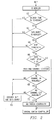
- the flowchart is given in Figure 8.
- index i is set to "0".
- P G finds a gap in which to transmit the data burst t ' DB +Q i .
- P M finds an unscheduled channel in P M to transmit the data burst at t' DB +Q i .
- the operations of finding a gap in P G to transmit the DB at time t' DB + Q i and finding an unscheduled time in P M to transmit the DB at time t' DB +Q i are preferably performed in parallel.
- the operation of finding a gap in P G to transmit the data burst at time t' DB +Q i (block 102) includes parallel comparison of each entry in P G with ( t' DB +Q i , t ' DB +Q i +l DB ) .
- the response bit of entry j returns 1, otherwise it returns 0, 0 ⁇ j ⁇ G - 1. If at least one entry in P G returns 1, the gap with the smallest index is selected.
- the operation finding an unscheduled time in P M to transmit the DB at time t' DB +Q i includes parallel comparison of each entry in P M with t' DB +Q i . If t' DB +Q i ⁇ t j , the response bit of entry j returns 1, otherwise it returns 0, 0 ⁇ j ⁇ K - 1 . If at least one entry in P M returns 1, the entry with the smallest index is selected.
- the CP 1 will inform the BHP processor 82 of the selected outgoing data channel and the FDL identifier in blocks 105 or 109, respectively. After receiving an ACK from the BHP processor 82, the CP 1 94 will update P G 90 or P M 94 or both. If scheduling is not successful, i is incremented in block 110, and P M and P G try to a time to schedule the data burst at a different delay. Once Q i reaches the maximum delay (decision block 112), the processors P M and P G report that the data burst cannot be scheduled in block 114.
- LAUC-VF first fit with void filling
- FF-VF first fit with void filling
- the block diagram of the CCS module 86 is shown in Figure 9. Similar to the DCS module 84, associative processor P T 120 keeps track of the usage of the control channel. Since a maximum of P f bytes of payload can be transmitted per frame, memory T 121 of P T 120 tracks only the number of bytes available per frame ( Figure 10). Relative time is used here as well.
- the CCS module 86 has two b 1 -bit frame counters, C f and C f / 1. C f counts the time frames. C f / 1 records the elapsed frames since the receiving of the last BHP.
- the basic idea is to send the BHP as earlier as possible, but the offset time should be no larger than ⁇ 0 (as described in connection with Figures 4a and 4b).
- J ⁇ 0 / T f ⁇ .
- J 8.
- J 2.
- the BHP length is X bytes.
- a constrained earliest time (CET) method is used for scheduling the control channel, as shown in Figure 11.
- P T 120 performs a parallel comparison of X (i.e., the length of a BHP) with the contents B t-j of relevant entries of memory T 121, E t-j , 0 ⁇ j ⁇ J - 1 and t - j > 0. If X ⁇ B t-j , entry E t-j returns 1, otherwise it returns 0.
- step 132 if at least one entry in P T returns 1, the entry with the smallest index is chosen in step 134. The index is stored and the CCS module 86 reports that a frame to send the BHP has been found. If no entry in P T returns a "1", then a negative acknowledgement is sent to the BHP processor 82. (step 136)
- the actual frame t f that the BHP will be sent out is ( t f DB - j + 2 b 1 ) mod 2 b 1 if E t-j is chosen.
- the new burst offset-time is ( t DB mod T f ) + j ⁇ T f .
- the CCS module 86 sends the BHP processor 82 the information on whether the BHP can be scheduled and in which time frame it will be sent. Once it gets an ACK from the BHP processor 82, the CCS module 86 will update P T . For example, if the content in entry y needs to be updated, then B y ⁇ B y - X . If the BHP cannot be scheduled, the CCS module 86 will send a NACK to the BHP processor 82. In the real implementation, the contents in P T do not have to move physically. A pointer can be used to record the entry index associated with the reference time frame 0.
- a block diagram of the path & channel selector 44 is shown in Figure 12.
- the function of the path & channel selector 44 is to control the access to the RxR RB switch 26 and to instruct the RB switch controller 28 and the spatial switch controller 30 to configure the respective switches 26 and 24.
- the path & channel selector 44 includes processor 140 coupled to a recirculation-buffer-in scheduling (RBIS) module 142, a recirculation-buffer-out scheduling (RBOS) module 144 and a queue 146.
- RBIS recirculation-buffer-in scheduling
- RBOS recirculation-buffer-out scheduling
- the RBIS module 142 keeps track of the usage of the R incoming channels to the RB switch 26 while the RBOS module 144 keeps track of the usage of the R outgoing channels from the RB switch 26.
- Any scheduling method can be used in RBIS and RBOS modules 142 and 144, e.g., LAUC-VF, FF-VF, LAUC, FF, etc.
- RBIS module 142 and RBOS module 144 may use the same or different scheduling methods. From manufacturing viewpoint, it is better that the RBIS and RBOS module use the same scheduling method as the DCS module 84. Without loss of generality, it is assumed here that the LAUC-VF method is used in both RBIS and RBOS modules 142 and 144; thus, the design of DCS module can be reused can be used for these modules.
- the processor 140 triggers the RBIS module 142 and RBOS module 144 simultaneously. It sends the information of t DB and l DB to the RBIS module 142, and the information of time-to-leave the OSM ( t DB + Q i ) and l DB to the RBOS module 144.
- the RBIS module 142 searches for incoming channels to the RB switch 26 which are idle for the time period of ( t DB , t DB + l DB ). If there are two or more eligible incoming channels, the RBIS module will choose one according to LAUC-VF.
- the RBOS module 144 searches for outgoing channels from the RB switch 26 which are idle for the time period of ( t DB + Q i , t DB + l DB + Q i ). If there are two or more eligible outgoing channels, the RBOS module 144 will choose one according to LAUC-VF.
- the RBIS (RBOS) module sends either the selected incoming (outgoing) channel identifier or NACK to the processor. If an eligible incoming channel to the RB switch 26 and an eligible outgoing channel from the RB switch 26 are found, the processor will send back ACK to both RBIS and RBOS module which will then update the channel state information. In the meantime, it will send ACK to the scheduler 42 and the configuration information to the two switch controllers 28 and 30. Otherwise, the processor 140 will send NACK to the RBIS and RBOS modules 142 and 144 and a NACK to the scheduler 42.
- the RBOS module 144 is needed because the FDL buffer to be used by a data burst is chosen by the scheduler 42, not determined by the RB switch 26. It is therefore quite possible that a data burst can enter the RB switch 26 but cannot get out of the RB switch 26 due to outgoing channel contention.
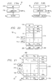
- An example is shown in Figure 13, where three fixed-length data bursts 148a-c arrive to the 2x2 RB switch 26. The first two data bursts 148a-b will be delayed 2D time while the third DB will be delayed D time. Obviously, these three data bursts will leave the switch at the same time and contend for the two outgoing channels. The third data burst 148c is lost in this example.
- the BHP transmission module 46 is responsible for transmitting the BHP on outgoing control channel 52 in the time frame determined by the BHP processor 82. Since the frame payload is fixed, equal P f , in slotted transmission, one possible implementation is illustrated in Figure 14, where the whole memory is divided into W c segments 150 and BHPs to be transmitted in the same time frame are stored in one segment 150. W c is the control channel scheduling window, which equals to 2 b 1 . There is a memory pointer per segment (shown in segment W 0 , pointing to the memory address where a new BHP can be stored. To distinguish BHPs within a frame, the frame overhead should contain a field indicating the number of BHPs in the frame. Furthermore, each BHP should contain a length field indicating the packet length (e.g., in bytes), from the first byte to the last byte of the BHP.
- t c is the current time frame during which the BHP is received by the BHP transmission module and p c points to the current memory segment.
- the memory segment to store this BHP is calculated from ( p c + ( t f - t c + 2 b 1 ) mod 2 b 1 ) mod 2 b 1 .
- the recirculation channels are differentiated while in Figure 1b all the recirculation channels are equivalent, able to provide B different delays.
- the design of the SCU 32 is almost the same as described previously, except for the following changes: (1) the RBOS module 144 within the path & channel selector 44 (see Figure 12) is no longer needed, (2) slight modification is required in the RBIS module 142 to distinguish recirculation channels if B > 1. To reduce the blocking probability of accessing the FDL buffer when B > 1, the scheduler is required to provide more than one delay option for each databurst that needs to be buffered. The impact on the design of scheduler and path & channel selector 44 is addressed below. Without loss of generality, it is assumed in the following discussion that the scheduler 42 has to schedule the databurst and the BHP for B+ 1 possible delays.
- DCS module 84 shown in Figure 5 remains valid in this implementation.
- the memory type (0/1) indicates P M or P G .
- the entry index gives the location in the memory, which will be used for information update later on.
- the channel identifier column gives the identifiers of the channels found.
- the DCS module then passes the indicator column and the channel identifier column (only those with indicator 1) to the BHP processor.
- CCS module 86 shown in Figure 9 also remains valid.
- the entry index gives the location in the memory, which will be used for information update later on.
- the "frame to send BHP" column gives the time frames in which the BHP are scheduled to send out.
- the CCS module then passes the indicator column and the "frame to send BHP" column (only those with indicator 1) to the BHP processor.
- the BHP processor 82 in Figure 3 After comparing the indicator columns from the DCS and CCS modules, the BHP processor 82 in Figure 3 knows whether the data burst and its BHP can be scheduled for a given FDL delay Q i , 1 ⁇ i ⁇ B and determines which configuration information will be sent to the path & channel selector 44 in Figure 12.
- the three possible scenarios are, (1) the data burst can be scheduled without using FDL buffer, (2) the data burst can be scheduled via using FDL buffer, and (3) the data burst cannot be scheduled.
- the data burst and its BHP are simply discarded.
- the following information will be sent to the path & channel selector: incoming DCG identifier, incoming data channel identifier, outgoing DCG identifier, outgoing data channel identifier, data burst arrival time to the spatial switch, data burst duration, FDL identifier 0 (i.e. Q 0 ).
- the path & channel selector 44 will immediately send back an ACK after receiving the information.
- the following information will be sent to the path & channel selector:
- the path & channel selector 44 will search for an idle buffer channel to carry the data burst.
- an idle buffer channel If an idle buffer channel is found, it will inform the processor 140, which in turn sends an ACK to the BHP processor 82.
- x 2
- both (P M1 , P G1 ) and (P M2 , P G2 ) will be searched. If two idle channels with different delays are found, the channel with delay Q 1 is chosen. In this case, an ACK together with the information that Q 1 is chosen will be sent to the BHP processor 82.
- the RBIS module 142 After a successful search, the RBIS module 142 will update the corresponding P M and P G pair.
- FIGS 17 - 26 illustrate variations of the LAUC-VF method, cited above.
- two associative processors P M and P G are used to store the status of all channels of the same outbound link.
- P M stores r words, one for each of the r data channels of an outbound link. It is used to record the unscheduled times of these channels.
- P G contains n superwords, one for an available time interval (a gap) of some data channel.
- the times stored in P M and P G are relative times.
- P M and P G support associative search operations, and data movement operations for maintaining the times in a sorted order. Due to parallel processing, P M and P G are used as major components to meet stringent real-time channel scheduling requirement.
- a pair of associative processors P M and P G for the same outbound link are combined into one associative processor P MG .
- the advantage of using a unified P MG to replace a pair of P M and P G is the simplification of the overall core router implementation. In terms of ASIC implementation, the development cost of a P MG can be much lower than that of a pair of P M and P G . P MG can be used to implement a simpler variation of the LAUC-VF method with faster performance.
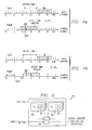
- FIGs 17a and 17b two outbound channels Ch 1 and Ch 2 are shown, with t 0 being the current time.
- channel Ch 1 has two DBs, DB 1 and DB 2 , scheduled and channel Ch 2 has DB 3 scheduled.
- the time between DB 1 and DB 2 on Ch 1 which is a maximal time interval that is not occupied by any DB, is called a gap.
- the times labeled t 1 and t 2 are the unscheduled time for Ch 1 and Ch 2 , respectively.
- Ch 1 and Ch 2 are available for transmitting any DB, respectively.
- the LAUC-VF method tries to schedule DBs according to certain priorities. For example, suppose that a new data burst DB 4 arrives at time t'. For the situation of Figure 17a, DB 4 can be scheduled within the gap on Ch 1 , or on Ch 2 after the unscheduled time of Ch 2 . The LAUC-VF method selects Ch 1 for DB 4 , and two gaps are generated from one original gap. For the situation of Figure 17b, DB 4 conflicts with DB 1 on Ch 1 and conflicts with DB 3 on Ch 2 . But by using FDL buffers, it may be scheduled for transmission without conflicting DBs on Ch 1 and/or DBs on Ch 2 . Figure 17b shows the scheduling that DB 4 is assigned to Ch 2 , and a new gap is generated.
- the two associative processors P M and P G were proposed to represent S M and S G , respectively. Due to fixed memory word length, the times stored in the associative memory M of P M and the associative memory G of P G are relative times. Suppose the current time is t 0 . Then any time value less than t 0 is of no use for scheduling a new DB.
- S' M ⁇ (max ⁇ t i - t 0 , 0 ⁇ , i )
- S' G ⁇ (max ⁇ l j - t 0 , 0 ⁇ , max ⁇ l j - t 0 , 0 ⁇ , c j )
- the times in S' M and S' G are times relative to the current time t 0 , which is used as a reference point 0.
- M of P M and G of P G are actually used to store S' M and S' G respectively.
- the channel scheduler proposed in U.S. Ser. No. 09/689,584 assumes that DBs have arbitrary lengths.
- One possibility is to assume a slot transmission mode. In this mode, DBs are transmitted in units of slots, and BHPs are transmitted as groups, and each group is carried by a slot.
- a slot clock CLK s is used to determine the slot boundary.
- the slot transmissions are triggered by pulses of CLK s .
- the relative time is represented in terms of number of CLK s cycles.
- the pulses of CLK s are shown in Figure 18.
- there is another finer clock CLK f In addition to clock CLK s , there is another finer clock CLK f .
- the period of CLK s is a multiple of the period CLK f .
- one CLK s cycle contains sixteen CLK f cycles.
- Clock CLK f is used to coordinate operations performed within a period of CLK s .
- FIG. 19b An alternative design, shown in Figure 19b, is to implement each word M i in M as a decrement counter with parallel load.
- the counter is decremented by 1 by every pulse of the system slot clock CLK s .
- the counting stops when the counter reaches 0, and the counting resumes once the counter is set to a new positive value.
- t' - ( t 1 - t 0 ) ⁇ 0) with the new reference point t 1 is not useful in the lookahead channel scheduling.
- a comparator 204 Associated with each word M i is a comparator 204. It is used for the parallel comparison operation.
- a word of G in P G can be implemented by two decrement counters with two associated comparators.
- the system has a c-bit circular increment counter C s .
- the value of C s is incremented by 1 by every pulse of slot clock CLK s .
- t latency (BHP i ) be the time, in terms of number of S' G cycles, between the time BHP i is received by the router and the time BHP i is received by the channel scheduler.
- the value c is chosen such that: where MAX s is the number of CLK f cycles within a CLK s cycle.
- BHP i is timestamped by operations timestamp recv (BHP i ) ⁇ C s .
- BHP i When BHP i is received by the scheduler of the router, BHP i is timestamped again by timestamp sch (BHP i ) ⁇ C s .
- D i (timestamp recv (BHP i ) + 2 c - timestamp sch (BHP i )) mod 2 c .
- associative processors P M and P G are used to store and process S' M and S' G , respectively.
- S' M ⁇ (t i , i)
- S' G ⁇ (l j , r j , c j )
- a pair ( t i , i) in S' M represents the unscheduled time on channel Ch i
- a triple (l j , r j , c j ) in S' G represents a time gap (interval) [l j , r j ] on channel Ch cj .
- the unscheduled time t i can be considered as a semi-infinite gap (interval) [t i , ⁇ ].
- S' M is no longer needed.
- S' M ⁇ (t i , ⁇ , i )
- S' MG S" M ⁇ S' G .
- the basic idea of combining P M and P G is to build P MG by modifying P G so that P MG is used to process S' MG .
- P MG uses an associative memory MG to store pairs in S' M and triples in S' G .
- each word of MG has two sub-words, with the first one for l j and second one for r j when it is used to store (l j , r j , c j ).
- a word of MG is used to store a pair (t i , i ) of S' M
- the first sub-word is used for t i
- the second is left unused.
- the first r words are reserved for S' M
- the remaining words are reserved for S' G .
- the first r words are maintained in non-increasing order of their first sub-word.
- the remaining words are also maintained in non-increasing order of their first subword.
- New operations for P MG are defined.
- P M and P G are summarized, and the structure and operations of P MG are defined.
- the differences between P MG include the number of address registers used, the priority encoders, and operations supported. It is shown that P MG can be used to implement the LAUC-VF method without any slow-down, in comparison with the implementation using P M and P G .
- the outbound data channel of a core router has r channels (wavelengths) for data transmission. These channels are denoted by Ch 1 , Ch 2 , .., Ch r .
- S ⁇ t i
- t i is the unscheduled time for channel Ch i .
- T" t j
- channel Ch j is considered as a candidate data channel for transmitting a DB at time T'.
- Associative processor P M includes an associative memory M 212 of k words, M 1 , M 2 , ..., M k , one for each channel of the data channel group. Each word is associated with a simple subtraction circuit for subtraction and compare operations. The words are also connected as a linear array. Comparand register MC 214 holds the operand for comparison. MCH 216 is a memory of k words, MCH 1 , MCH 2 , ..., MCH k , with MCH j corresponding to M j . The words are connected as a linear array, and they are used to hold the channel numbers.
- MAR 1 218 and MAR 2 220 are address registers for holding addresses for accessing M and MCH.
- MDR 222 and MCHR 224 are data registers used to access M and MCHR along with the MARs.
- Associative processor P M supports the following major operations that are used in the efficient implementation of the LAUC-VF channel scheduling operations:
- each pair (M j , MCH j ) is treated as a superword.
- the output of PARALLEL-SEARCH consists r binary signals, MFLAG i , 1 ⁇ i ⁇ r.
- MFLAG i 1 if and only if M i ⁇ MC.
- RANDOM-READ, RANDOM-WRITE, PARALLEL-SEARCH and SEGMENT-SHIFT-DOWN operations are used to maintain the non-increasing order of values stored in M .
- Figure 21 illustrates a block diagram of the associative processor P G 92.
- a P G is used to store unused gaps of all channels of an outbound link of a core router.
- a gap is represented by a pair ( l , r) of integers, where l and r are the beginning and the end of the gap, respectively.
- Associative processor P G includes associative memory G 93, comparand register GC 230, memory GCH 232, address register GAR 234, data registers GDR 236 and GCHR 238 and working registers GR 1 240 and GR 2 242.
- G is an associative memory of n words, G 1 , G 2 ..., G n , with each G i consisting of two sub-words G i,1 and G i,2 .
- the words are connected as a linear array.
- GC holds a word of two sub-words, GC 1 and GC 2 .
- GCH is a memory of n words, GCH 1 , GCH 2 , ..., GCH n with GCH j corresponding to G j .
- the words are connected as a linear array, and they are used to hold the channel numbers.
- GAR is an address register used to hold address for accessing G.
- GDR, and GCHR are data registers used to access M and MCHR, together with GAR.
- Associative processor P G supports the following major operations that are used in the efficient implementation of the LAUC-VF channel scheduling operations:
- a triple ( G i,1 ,G i,2 ,GCH i ) corresponds to a gap with beginning time G i,1 and ending time G i,2 on channel GCH i .
- each triple ( G i,1 ,G i,2 ,GCH i ) is treated as a superword.
- the output of PARALLEL-DOUBLE-COMPARAND-SEARCH (resp.
- RANDOM-WRITE, PARALLEL-SINGLE-COMPARAND-SEARCH, BIPARTITION-SHIFT-UP, and BIPARTITION-SHIFT-DOWN operations maintain the non-increasing order of values stored in G i,1 s.
- FIG 22 illustrates a block diagram of a processor P MG , which combines the functions of the P M and P G processors described above.
- P MG includes associative memory MG 248, comparand register MGC 250, memory MGCH 252, address registers MGAR 1 254a and MGAR 2 254b, and data registers MGDR 256 and MGCHR 258.
- the words are also connected as a linear array.
- MGC is a comparand register that holds a word of two sub-words, MGC 1 and MGC 2 .
- MGC also holds a word of two sub-words, MGC 1 and MGC 2 .
- MGCH is a memory of m words, MGCH 1 ,MGCH 2 ,..., MGCH m with MGCH j corresponding to MG j .
- the words are connected as a linear array, and they are used to hold the channel numbers.
- Associative processor P MG supports the following major operations:
- a triple ( MG i,1 , MG i,2 , MGCH i ) may correspond to a gap with beginning time MG i,1 and ending time MG i,2 on channel MGCH i . But in such a case, it must be that i > r. If i ⁇ r, then MG i,2 is immaterial, the pair (MG i,1 , MGCH i ) is interpreted as the unscheduled time MG i,1 on channel MGCH i , and this pair corresponds to a word in P M .
- each triple (MG i , 1 , MG i , 2 ,..., MGCH i ) is treated as a superword.
- the first r superwords are used for storing the unscheduled times of r outbound channels, and the last m - r superwords are used to store information about gaps on all outbound channels.
- the first one uses MGFLAG i , 1 ⁇ i ⁇ r, as its input, and it produces an address in MGAR 1 after a PARALLEL-COMPOUND-SEARCH operation is performed if MGC 2 ⁇ 0.
- the second encoder uses MGFLAG i , r + 1 ⁇ i ⁇ m, as its input. It produces an address in MGAR 2 after a PARALLEL-COMPOUND-SEARCH operation is performed if MGC 2 ⁇ 0.
- MGC 2 0, the smallest non-zero address produced by the two encoders, if such an address exists, Ys loaded into MGAR 1 after a PARALLEL-COMPOUND-SEARCH operation is performed; otherwise, MGAR 1 is set to 0 after a PARALLEL-COMPOUND-SEARCH operation is performed; If MGC 2 ⁇ 0, the output of the selector is disabled.
- RANDOM-READ, RANDOM-WRITE, PARALLEL-COMPOUND-SEARCH1, BIPARTITION-SHIFT-UP and SEGMENT-SHIFT-DOWN operations are used to maintain the non-increasing order of values stored in MG i,1 of the first m words, and the non-increasing order of the values stored in MG i,1 of the last m - r words.
- the operations of associative processors P M and P G can be carried out by operations of P MG without any delay when they are used to implement LAUC-VF channel scheduling method.
- Table 3 the operations of P M (resp. P G ) given in the left column are carried out by operations of P MG given the right column.
- this step can be carried out by PARALLEL-COMPOUND-SEARCH operation.
- P* MG and P MG differ in their priorities.
- MG is searched. The fitting time interval found, regardless if it is a gap or a semi-infinite interval, will be used for the new DB. Once the DB is scheduled, one more gap may be generated. As long as there is sufficient space in MG, the new gap is stored in MG. When MG is full, an item of S' G may be lost. But it is enforced that all items of S' M must be kept.
- t s out (DB i ) and t e out (DB i ) be the transmitting time of the first and last slot of DB i at the output of the router, respectively.
- t s out (DB i ) T i + L j
- t e out (DB i ) T i + L j + length(DB i )
- T i is the relative arrival time defined above
- L j is the FDL delay time selected for DB i in the switching matrix
- length(DB 2 ) is the length of DB i in terms of number of slots.
- L 0 0 ⁇ L 1 ⁇ L 2 ⁇ ... ⁇ L q-i ⁇ L q .
- the new variation of LAUC-VF is sketched as follows:
- MG is updated.
- TYPE m 1, the new gap is ignored. This ensures that no item belonging to S' M is lost.
- Associative processor P* MG supports the following major operations:
- the value of TYPE indicates the type of information stored in MG i .
- each quadruple (MG i,1 , MG i,2 , TYPE;, MGCH i ) is treated as a superword.
- RANDOM-READ RANDOM-WRITE
- PARALLEL-COMPOUND-SEARCH PARALLEL-COMPOUND-SEARCH
- BIPARTITION-SHIFT-UP BIPARTITION-SHIFT-UP and SEGMENT-SHIFT-DOWN operations are used to maintain the non-increasing order of values stored in MG i , 1 s.
- Figure 24 illustrates the use of multiple associative processors for fast scheduling.
- Channel scheduling for an OBS core router is very time critical, and multiple associative processors (shown in Figure 24 as P* MG processors 270), which are parallel processors, are proposed to implement scheduling methods.
- P* MG processors 270 which are parallel processors.
- L 0 0, L 1 , ..., L q in the DB switching matrix such that L 0 ⁇ L 1 ⁇ ... ⁇ L q .
- These FDLs are used, when necessary, to delay DBs and increase the possibility that the DBs can be successfully scheduled.
- the same pair of P M and P G are searched repeatedly using different FDLs until a scheduling solution is found or all FDLs are exhausted.
- the method CHANNEL-SCHEDULING described above uses the same idea.
- a scheduler 42 may use q + 1 P M / P G pairs, one for each L i .
- all q + 1 Ms have the same content
- all q + 1 MCHs have the same content
- all q + 1 G s have the same content
- all q + 1 GCHs have the same content. Then finding a scheduling solution for all different FDLs can be performed on these P M / P G pairs simultaneously. At most one search result is used for a DB.
- All P M / P G pairs are updated simultaneously by the same lock-step operations to ensure that they store the same information.
- one may use q + 1 P MG s or P* MG s to speed up the scheduling.
- a multiple processor system 300 uses q + 1 P* MG s 270 implement the method CHANNEL-SCHEDULING described above.
- the LAUC-VF method can be implemented using multiple P M / P G pairs, or multiple P MG s in a similar way to achieve better performance.
- the multiple P* MG s 270 include q + 1 associative memories MG 0 , MG 1 ,..., MG q .
- Each MG j has m words MG j 1 , MG j 2 , ..., MG j m , with each MG j i consisting of two sub-words MG j i,1 and MG j i,2 .
- Each MGC j holds a word of two sub-words, MGC j 1 and MGC j 2 .
- MGCHs There are q + 1 associative memories MGCH 0 , MGCH 1 ,..., MGCH q .
- Each MGCH j has m words, MGCH j 1 , MGCH j 2 , ..., MGCH j m .
- the words in MGCHi are connected as a linear array.
- MGAR 1 MGAR are address registers used to hold address for accessing MG and MGCH.
- MGDR, TYPER, MGCH are: data registers used to access MGs, TYPEs and MGCHR.
- This multiple processor system 300 supports the following major operations:
- a RANDOM-READ operation is performed on one copy of P* MG , i.e. MG 0 , TYPE 0 , and MGC j .
- RANDOM-WRITE, PARALLEL-COMPOUND-SEARCH, BIPARTITION-SHIFTUP and SEGMENT-SHIFT-DOWN operations are performed on all copes of P* MG .
- each quadruple MG i,1 , MG i,2 , TYPE i , MGCH i
- the output of all P* MG copies are the input of selectors. The output of one P* MG copy is selected.
- the CHANNEL-SCHEDULING method may be implemented in the multiple processor system as:
- group partition feature into channel scheduling associative processors, the basic idea is to associate a group identifier (or gid for short) with each channel. For a link, all the channels share the same gid belong to the same group.
- the gid of a channel is programmable; i.e. it can be changed dynamically according to need.
- the gid for a DB can be derived from its BHP and/or some other local information.
- P M and P G to P M-ext and P G-ext may be extended to incorporate multiple channel groups, as shown in Figures 25 and 26, respectively.
- associative processor P M-ext 290 includes M, MC, MCH, MAR 1 , MAR 2 , MDR, MCHR, as described in connection with Figure 20.
- MCIDC 292 is a comparand register that holds the gid for comparison.
- MGID 294 is a memory of r words, MGID 1 , MGID 2 , ..., MGID r , with MGID j corresponding to M j and MCH j . The words are connected as a linear array, and they are used to hold the channel group numbers.
- MGIDDR 296 is a data register.
- P M-ext is similar to P M with the addition of several components, and modifying operations.
- the linear array MGID has r locations, MGID 1 , MGID 2 ,..., MGID r ; each is used to store an integer gid.
- MGID i is associated with M i and MCH i , i.e. a triple (M i , MCH i , MGID i ) is treated as a superword.
- Comparand register MGIDC and data register MGIDDR are added.
- Associative processor P M-ext supports the following major operations that are used in the efficient implementation of the LAUC-VF channel scheduling operations.
- each triple (M j , MCH j , MGID j ) is treated as a superword.
- the output of PARALLEL-SEARCH1 consists r binary signals, MFLAG i , 1 ⁇ i ⁇ r.
- the output of PARALLEL-SEARCH2 consists r binary signals, MFLAG i , 1 ⁇ i ⁇ r.
- the same priority encoder used in PARALLEL-SEARCH 1 transforms MFLAG i , 1 ⁇ i ⁇ r, into an address j and this value is loaded into MAR 1 when PARALLEL-SEARCH operation is completed.
- RANDOM-READ, RANDOM-WRITE, PARALLEL-SEARCH2 and SEGMENT-SHIFT-DOWN operations are used to maintain the non-increasing order of values stored in M.
- FIG 26 illustrates a block diagram of P G-ext .
- P G-ext 300 includes G,GC,GCH,GAR,GDR,GCHR, as described in connection with Figure 21.
- GGIDC 302 is a comparand register for holding the gid for comparision.
- GGID 304 is a memory of r words, GGID 1 , GGID 2 , ..., GGID r , with GGID j corresponding to G j and GCH j . The words are connected as a linear array, and they are used to hold the channel group numbers.
- GGIDR 306 is a data register.
- a linear array GGID of n words GGID 1 , GGID 2 , ..., GGID n is added to P G .
- a quadruple (G i,1 , G i,2 , MCH i , GGID i ) is treated as a superword.
- Associative processor P G-ext supports the following major operations that are used in the efficient implementation of the LAUC-VF channel scheduling operations.
- a quadruple (G i,1 , G i,2 , GCH i , GGID i ) corresponds to a gap with beginning time G i,1 and ending time G i,2 on channel CCH i , whose gid is in GGID i .
- each quadruple ( G i , 1 , G i,2 , GCH i , GGID i ) is treated as a superword.
- the scheduling of DB' involves searches in P M-ext and P G-ext .
- P G-ext and P G * -ext can be constructed by adding a gid comparand register MGGIDC, a memory MGGID of m words MGGID 1 , MGGID 2 ,, MGGIDm, and a data register MGGIDDR.
- P MG-ext is a combination of P M- ext and P G-ext .
- the operations of P MG-ext can be easily derived from the operations of P M- ext and P G-ext since the P M-ext items and the P G-ext items are separated.
Landscapes
- Engineering & Computer Science (AREA)
- Computer Networks & Wireless Communication (AREA)
- Data Exchanges In Wide-Area Networks (AREA)
- Optical Communication System (AREA)
Abstract
An optical switch network (4) includes optical routers (10), which route
information in optical fibers (12). Each fiber carries a plurality of data channels (20),
collectively a data channel group (14), and a control channel (16). Data is carried on
the data channels in data bursts and control information is carried on the control
channel (18) in burst header packets. A burst header packet includes routing
information for an associated data burst (28) and precedes its associated data burst.
Parallel scheduling at multiple delays may be used for faster scheduling. In one
embodiment, unscheduled times and gaps may be processed in a unified memory for
more efficient operation.
Description
This application claims the benefit of the filing date of copending provisional
application U.S. Ser. No. 60/257,884, filed December 22, 2000, entitled "Unified
Associative Memory of Data Channel Schedulers in an Optical Router" to Zheng et
al.
This invention relates in general to telecommunications and, more
particularly, to a method and apparatus for optical switching.
Data traffic over networks, particularly the Internet, has increased
dramatically recently, and will continue as the user increase and new services
requiring more bandwidth are introduced. The increase in Internet traffic requires a
network with high capacity routers capable of routing data packets of variable
length. One option is the use of optical networks.
The emergence of dense-wavelength division multiplexing (DWDM)
technology has improved the bandwidth problem by increasing the capacity of an
optical fiber. However, the increased capacity creates a serious mismatch with
current electronic switching technologies that are capable of switching data rates up
to a few gigabits per second, as opposed to the multiple terabit per second capability
of DWDM. While emerging ATM switches and IP routers can be used to switch data
using the individual channels within a fiber, typically at a few hundred gigabits per
second, this approach implies that tens or hundreds of switch interfaces must be
used to terminate a single DWDM fiber with a large number of channels. This could
lead to a significant loss of statistical multiplexing efficiency when the parallel
channels are used simply as a collection of independent links, rather than as a shared
resource.
Different approaches advocating the use of optical technology in place of
electronics in switching systems have been proposed; however, the limitations of
optical component technology has largely limited optical switching to facility
management/control applications. One approach, called optical burst-switched
networking, attempts to make the best use of optical and electronic switching
technologies. The electronics provides dynamic control of system resources by
assigning individual user data bursts to channels of a DWDM fiber, while optical
technology is used to switch the user data channels entirely in the optical domain.
Previous optical networks designed to directly handle end-to-end user data
channels have been disappointing.
Therefore, a need has arisen for a method and apparatus for providing an
optical burst-switched network.
In the present invention, an optical burst-switched router comprises an optical
switch for routing optical information from an incoming optical transmission
medium to one of a plurality of outgoing optical transmission media, each outgoing
media able to transmit optical information over a plurality of channels. A delay
buffer is coupled to the optical switch for providing a plurality of different delays for
delaying selected information between the incoming transmission medium and one
of the outgoing optical transmission media. Scheduling circuitry is associated with
each respective outgoing medium, comprising an associative processor for storing
information on both unscheduled time for each channel and time gaps on each
channel on the respective outgoing medium.
The present invention provides an efficient architecture for identifying
unscheduled time and time gaps within which a data burst can be scheduled.
For a more complete understanding of the present invention, and the
advantages thereof, reference is now made to the following descriptions taken in
conjunction with the accompanying drawings, in which:
The present invention is best understood in relation to Figures 1 - 26 of the
drawings, like numerals being used for like elements of the various drawings.
Figure 1a illustrates a general block diagram of an optical burst switched
network 4. The optical burst switched (OBS) network 4 includes multiple electronic
ingress edge routers 6 and multiple egress edge routers 8. The ingress edge routers 6
and egress edge routers 8 are coupled to multiple core optical routers 10. The
connections between ingress edge routers 6, egress edge routers 8 and core routers 10
are made using optical links 12. Each optical fiber can carry multiple channels of
optical data.
In operation, a data burst (or simply "burst") of optical data is the basic data
block to be transferred through the network 4. Ingress edge routers 6 and egress
edge routers 8 are responsible for burst assembly and disassembly functions, and
serve as legacy interfaces between the optical burst switched network 4 and
conventional electronic routers.
Within the optical burst switched network 4, the basic data block to be
transferred is a burst, which is a collection of packets having some common
attributes. A burst consists of a burst payload (called "data burst") and a burst
header (called "burst header packet" or BHP). An intrinsic feature of the optical burst
switched network is that a data burst and its BHP are transmitted on different
channels and switched in optical and electronic domains, respectively, at each
network node. The BHP is sent ahead of its associated data burst with an offset time
τ (≥ 0). Its initial value, τ0, is set by the (electronic) ingress edge router 8.
In this invention, a "channel" is defined as a certain unidirectional
transmission capacity (in bits per second) between two adjacent routers. A channel
may consist of one wavelength or a portion of a wavelength (e.g., when time-division
multiplexing is used). Channels carrying data bursts are called "data channels", and
channels carrying BHPs and other control packets are called "control channels". A
"channel group" is a set of channels with a common type and node adjacency. A link
is defined as a total transmission capacity between two routers, which usually
consists of a "data channel group" (DCG) and a "control channel group" (CCG) in
each direction.
Figure 1b illustrates a block diagram of a core optical router 10. The incoming
DCG 14 is separated from the CCG 16 for each fiber 12 by demultiplexer 18. Each
DCG 14 is delayed by a fiber delay line (FDL) 19. The delayed DCG is separated into
channels 20 by demultiplexer 22. Each channel 20 is input to a respective input node
on a non-blocking spatial switch 24. Additional input and output nodes of spatial
switch 24 are coupled to a recirculation buffer (RB) 26. Recirculation buffer 26 is
controlled by a recirculation switch controller 28. Spatial switch 24 is controlled by a
spatial switch controller 30.
The embodiment shown in Figure 1b has N input DCG-CCG pairs and N
output DCG-CCG pairs 52, where each DCG has K channels and each CCG has only
one channel (k=1). A DCG-CCG pair 52 is carried in one fiber. In general, the optical
router could be asymmetric, the number of channels k of a CCG 16 could be larger
than one, and a DCG-CCG pair 52 could be carried in more than one fiber 12. In the
illustrated embodiment, there is one buffer channel group (BCG) 56 with R buffer
channels. In general, there could be more than one BCG 56. The optical switching
matrix (OSM) consists of a (NK+R)x(NK+R) spatial switch and a RxR switch with
WDM (wavelength division multiplexing) FDL buffer serving as recirculation buffer
(RB) 26 to resolve data burst contentions on outgoing data channels. The spatial
switch is a strictly non-blocking switch, meaning that an arriving data burst on an
incoming data channel can be switched to any idle outgoing data channel. The delay
Δ introduced by the input FDL 19 should be sufficiently long such that the SCU 32
has enough time to process a BHP before its associated data burst enters the spatial
switch.
The RxR RB switch is a broadcast-and-select type switch of the type described
in P. Gambini, et al., "Transparent Optical Packet Switching Network Architecture
and Demonstrators in the KEOPS Project", IEEE J. Selected Areas in Communications,
vol. 16, no. 7, pp. 1245-1259, Sept. 1998. It is assumed that the RxR RB switch has B
FDLs with the ith FDL introducing Qi delay time, 1 ≤ i ≤ B. It is further assumed
without loss of generality that Q 1 < Q 2 <...< QB and Q 0 = 0, meaning no FDL buffer is
used. Note that the FDL buffer is shared by all N input DCGs and each FDL contains
R channels. A data burst entering the RB switch on any incoming channel can be
delayed by one of B delay times provided. The recirculation buffer in Figure 1b can
be degenerated to passive FDL loops by removing the function of RB switch, as
shown in Figure 15, wherein different buffer channels may have different delays.
The SCU is partially based on an electronic router. In Figure 1b, the SCU has N
input control channels and N output control channels. The SCU mainly consists of
packet processors (PPs) 36, forwarders 38, a switching fabric 40, schedulers 42, BHP
transmission modules 46, a path & channel selector 44, a spatial switch controller 30,
and a RB switch controller 28. The packet processor 36, the forwarders 38, and the
switching fabric 40 can be found in electronic routers. The other components,
especially the scheduler, are new to optical routers. The design of the SCU uses the
distributed control as much as possible, except the control to the access of shared
FDL buffer which is centralized.
The packet processor performs layer 1 and layer 2 decapsulation functions and
attaches a time-stamp to each arriving BHP, which records the arrival time of the
associated data burst to the OSM. The time-stamp is the sum of the BHP arrival time,
the burst offset-time τ carried by the BHP and the delay Δ introduced by input FDL
19. The forwarder mainly performs the forwarding table lookup to decide which
outgoing CCG 52 to forward the BHP. The associated data burst will be switched to
the corresponding DCG 54. The forwarding can be done in a connectionless or
connection-oriented manner.
There is one scheduler for each DCG-CCG pair 52. The scheduler 42 schedules
the switching of the data burst on a data channel of the outgoing DCG 54 based on
the information carried by the BHP. If a free data channel is found, the scheduler 42
will then schedule the transmission of the BHP on the outgoing control channel,
trying to "resynchronize" the BHP and its associated data burst by keeping the offset
time τ (≥ 0) as close as possible to τ0. After both the data burst and BHP are
successfully scheduled, the scheduler 42 will send the configuration information to
the spatial switch controller 30 if it is not necessary to provide a delay through the
recirculation buffer 26, otherwise it will also send the configuration information to
the RB switch controller 28.
The data flow of scheduling decision process is shown in Figure 2. In decision
block 60, the scheduler 42 determines whether or not there is enough time to
schedule an incoming data burst. If so, the scheduler determines whether the data
burst can be scheduled, i.e., whether there is an unoccupied space in the specified
output DCG 54 for the data burst. In order to schedule the data burst, there must be
an available space to accommodate the data burst in the specified output DCG. This
space may start within a time window beginning at the point of arrival of the data
burst at the spatial switch 24 extending to the maximum delay which can be
provided by the recirculation buffer 26. If the data burst can be scheduled, then the
scheduler 42 must determine whether there is a space available in the output CCG 52
for the BHP in decision block 64.
If any of the decisions in decision blocks 60, 62 or 64 are negative, the data
burst and BHP are dropped in block 65. If all of the decisions in decision blocks 60,
62 and 64 are positive, the scheduler sends the scheduling information to the path
and channel selector 44. The configuration information from scheduler to path &
channel selector includes incoming DCG identifier, incoming data channel identifier,
outgoing DCG identifier, outgoing data channel identifier, data burst arrival time to
the spatial switch, data burst duration, FDL identifier i (Qi delay time is requested,
0 ≤ i ≤ B).
If the FDL identifier is 0, meaning no FDL buffer is required, the path &
channel selector 44 will simply forward the configuration information to the spatial
switch controller 30. Otherwise, the path & channel selector 44 searches for an idle
incoming buffer channel to the RB switch 26 in decision block 68. If found, the path
and channel selector 44 searches for an idle outgoing buffer channel from the RB
switch 26 to carry the data burst reentering the spatial switch after the specified delay
inside the RB switch 26 in decision block 70. It is assumed that once the data burst
enters the RB switch, it can be delayed for any discrete time from the set {Q 1, Q 2, ...,
QB }. If this is not the case, the path & channel selector 44 will have to take the RB
switch architecture into account. If both idle channels to and from the RB switch 26
are found, the path & channel selector 44 will send configuration information to the
spatial switch controller 30 and the RB switch controller 28 and send an ACK
(acknowledgement) back to the 42 scheduler. Otherwise, it will send a NACK
(negative acknowledgement) back to the scheduler 42 and the BHP and data burst
will be discarded in block 65.
Configuration information from the path & channel selector 44 to the spatial
switch controller 30 includes incoming DCG identifier, incoming data channel
identifier, outgoing DCG identifier, outgoing data channel identifier, data burst
arrival time to the spatial switch, data burst duration, FDL identifier i (Qi delay time
is requested, 0 ≤ i ≤ B). If i > 0, the information also includes the incoming BCG
identifier (to the RB switch), incoming buffer channel identifier (to the RB switch),
outgoing BCG identifier (from the RB switch), and outgoing buffer channel identifier
(from the RB switch).
Configuration information from path & channel selector to RB switch
controller includes an incoming BCG identifier (to the RB switch), incoming buffer
channel identifier (to the RB switch), outgoing BCG identifier (from the RB switch),
outgoing buffer channel identifier (from the RB switch), data burst arrival time to the
RB switch, data burst duration, FDL identifier i (Q i delay time is requested, 1 ≤ i ≤ B ).
The spatial switch controller 30 and the RB switch controller 28 will perform
the mapping from the configuration information received to physical components
that involved in setting up the internal path(s), and configure the switches just-in-time
to let the data burst fly-through the optical router 10. When the FDL identifier is
larger than 0, the spatial switch controller will set up two internal paths in the spatial
switch, one from the incoming data channel to the incoming recirculation buffer
channel when the data burst arrives to the spatial switch, another from the outgoing
buffer channel to the outgoing data channel when the data burst reenters the spatial
switch. Upon receiving the ACK from the path & channel selector 44, the scheduler
42 will update the state information of selected data and control channels, and is
ready to process a new BHP.
Finally, the BHP transmission module arranges the transmission of BHPs at
times specified by the scheduler.
The above is the general description on how the data burst is scheduled in the
optical router. Recirculating data bursts through the RxR recirculation buffer switch
more than once could be easily extended from the design principles described below
if so desired.
Figure 3 illustrates a block diagram of a scheduler 42. The scheduler 42
includes a scheduling queue 80, a BHP processor 82, a data channel scheduling (DCS)
module 84, and a control channel scheduling (CCS) module 86. Each scheduler needs
only to keep track of the busy/idle periods of its associated outgoing DCG 54 and
outgoing CCG 52.
BHPs arriving from the electronic switch are first stored in the scheduling
queue 80. For basic operations, all that is required is one scheduling queue 80,
however, virtual scheduling queues 80 may be maintained for different service
classes. Each queue 80 could be served according to the arrival order of BHPs or
according to the actual arrival order of their associated data bursts. The BHP
processor 82 coordinates the data and control channel scheduling process and sends
the configuration to the path & channel selector 44. It could trigger the DCS module
84 and the CCS module 82 in sequence or in parallel, depending on how the DCS and
CCS modules 84 and 82 are implemented.
In the case of serial scheduling, the BHP processor 82 first triggers the DCS
module 84 for scheduling the data burst (DB) on a data channel in a desired output
DCS 54. After determining when the data burst will be sent out, the BHP processor
then triggers the CCS module 86 for scheduling the BHP on an associated control
channel.
In the case of parallel scheduling, the BHP processor 82 triggers the DCS
module 84 and CCS module 86 simultaneously. Since the CCS module 86 does not
know when the data burst will be sent out, it schedules the BHP for all possible
departure times of the data burst or its subset. There are in total B+1 possible
departure times. Based on the actual data burst departure time reported from the
DCS module 84, the BHP processor 86 will pick the right time to send out the BHP.
Slotted transmission is used in data and control channels between edge and
core and between core nodes in the OBS network. A slot is a fixed-length time period.
Let Ts be the duration (e.g., in µs) of a time slot in data channels and Tf be the
duration of a time slot in control channels. Ts · rd Kbits of information can be sent
during a slot if the data channel speed is rd gigabits per second. Similarly, Tf · rc
Kbits of information can be sent during a slot if the control channel speed is rc
gigabits per second. Two scenarios are considered, (1) rc = rd and (2) rc ≠ rd. In the
latter case, a typical example is that rc = rd /4 (e.g., OC-48 is used in control channels
and OC-192 is used in data channels).
Without loss of generality, it is assumed that Tf is equal to multiples of Ts.
Two examples are depicted in Figures 4a and 4b (see also, Figure 18), which
illustrates the timestamp and burst offset-time in a slotted transmission system for
the cases where Tf = Ts and Tf = 4Ts , with the initial offset time τ0 = 8Ts . To simplify
the description, we use time frame to designate time slot in control channels. It is
further assumed without loss of generality that, (1) data bursts are variable length, in
multiple of slots, which can only arrive at slot boundaries, and (2) BHPs are also
variable length, in, for instance, multiple of bytes. Fixed-length data bursts and BHPs
are just special cases. In slotted transmission, there is some overhead in each slot for
various purposes like synchronization and error detection. Suppose the frame
payload on control channels is Pf bytes, which is less than (Tf · rc ). 1000/8 bytes, the
total amount of information can be transmitted in a time frame.
The OSM is configured periodically. For slotted transmission on data
channels, a typical example of the configuration period is one slot, although the
configuration period could also be a multiple of slots. Here it is assumed that the
OSM is configured every slot. The length of a FDL Qi needs also to be a multiple of
slots, 1 ≤ i ≤ B. Due to the slotted transmission and switching, it is suggested to use
the time slot as a basic time unit in the SCU for the purpose of data channel
scheduling, control channel scheduling and buffer channel scheduling, as well as
synchronization between BHPs and their associated data bursts. This will simplify
the design of various schedulers.
The following integer variables are used in connection with Figures 4a, 4b and
5:
Each arriving BHP to the SCU is time-stamped at the transceiver interface,
right after O/E conversion, recording the beginning of the time frame during which
the BHP enters the SCU. For the BHPs received by the SCU in the same time frame,
they will have the same timestamp tBHP. For scheduling purpose, the most important
variable is tDB, the DB arrival time to the OSM. Suppose a b-bit slot counter is used in
the SCU to keep track of time, tDB can be calculated as follows.
tDB = (tBHP · Tf + Δ+ τ) mod 2 b .
Timestamp tDB will be carried by the BHP within the SCU 32. Note that the
burst offset-time τ is also counted starting from the beginning of the time frame that
the BHP arrives as shown in Figures 4a-b, where in Figure 4a, tBHP = 9 and τ = 6 slots,
and in Figure 4b, tBHP = 2 and τ = 7 slots. Suppose Δ = 100 slots, we have tDB = 115,
meaning that the DB will arrive at slot boundary 115. In Figures 4a-b, 1 ≤ τ ≤ τ0 = 8. It
is assumed without loss of generality that the switching latency of the spatial switch
in Figure 1b is negligible. So the data burst arrival time tDB to the spatial switch 24 is
also its departure time if no FDL buffer is used. Note that even if the switching
latency is not negligible, tDB can still be used as the data burst departure time in
channel scheduling as the switching latency is compensated at router output ports
where data and control channels are resynchronized.
Figure 5 illustrates a block diagram of a DCS module 84. In this embodiment,
associative processor arrays P M 90 and P G 92 perform parallel searches of
unscheduled channel times and gaps between scheduled channel times and update
state information. Gaps and unscheduled times are represented in relative times. P M
90 and P G 92 are coupled to control processor CP 1 94. In one embodiment, a LAUC-VF
(Latest Available Unused Channel with Void Filling) scheduling principle is used
to determine a desired scheduling, as described in connection with U.S. Ser. No.
09/689,584, entitled "Hardware Implementation of Channel Scheduling Algorithms
of Optical Routers with FDL Buffers" to Zheng et al, filed October 12, 2000, and
which is incorporated by reference herein.
The DCS module 84 uses two b-bit slot counters, C and C1. Counter C keeps
track of the time slots, which can be shared with the CCS module 86. Counter C1
records the elapsed time slots since the last BHP is received. Both counters are
incremented by every pulse of the slot clock. However, counter C1 is reset to 0 when
the DCS module 84 receives a new BHP. Once counter C1 reaches 2b-1, it stops
counting, indicating that at least 2b-1 slots have elapsed since the last BHP. The value
of b should satisfy 2 b ≥ Ws where Ws is the data channel scheduling window.
Ws = τ 0 + Δ + QB + L max - δ, where L max is the maximum length of a DB and δ is the
minimum delay of a BHP from O/E conversion to the scheduler 42. Assuming that
τ0 = 8, Δ = 120, QB = 32, L max = 64, and δ = 40, then Ws = 184 slots. In this case, b = 8
bits.
Associative processor PM in Figure 5 is used to store the unscheduled time of
each data channel in a DCG. Let ti be the unscheduled time of channel Hi which is
stored in ith entry of P M 0 ≤ i ≤ K -1. Then from slot ti onwards, channel Hi is free,
i.e., nothing being scheduled. ti is a relative time, with respect to the time slot that
the latest BHP is received by the scheduler. PM has an associative memory of 2K
words to store the unscheduled times ti and channel identifiers, respectively. The
unscheduled times are stored in descending order. For example, in Figure 6 we have
K = 8 and t 0 ≥ t 1 ≥ t 2 ≥ t 3 ≥ t 4 ≥ t 5 ≥ t 6 ≥ t 7.
Similarly, associative processor PG in Figure 5 is used to store the gaps of data
channels in a DCG. We use lj and rj to denote the start time and ending time of gap
j, 0 ≤ j ≤ G - 1, which are also relative times. This gap is stored in jth entry of PG and
its corresponding data channel is Hj. PG has an associative memory of G words to
store the gap start time, gap ending time, and channel identifiers, respectively. Gaps
are also stored in the descending order according to their start times lj. For example,
Figure 7 illustrates the associative memory of PG, where l 0 ≥ l 1 ≥ l 2 ≥...≥ lG -2 ≥ lG -1. G is
the total number of gaps that can be stored. If there are more than G gaps, the newest
gap with larger start time will push out the gap with the smallest start time, which
resides at the bottom of the associative memory. Note that if lj = 0, then there are in
total j gaps in the DCG, as lj +1 = lj +2 =... = lG -1 = 0.
Upon receiving a request from the BHP processor to schedule a DB with
departure time tDB and duration lDB, the control processor (CP1) 94 first records the
time slot tsch during which it receives the request, reads counter C1 (te ← C 1) and
reset C1 to 0. Using tsch as a new reference time, the CP1 then calculates the DB
departure time (no FDL buffer) with respect to tsch as
t'DB = (tDB - tsch + 2 b ) mod 2 b ,
In the meantime, CP1 updates PM using
ti = max(0, ti - te ), 0 ≤ i ≤ K - 1
and updates PG using the following formulas,
lj = max(0, lj - te ), 0 ≤ j ≤ G - 1
and
rj = max(0, rj - te ), 0 ≤ j ≤ G - 1.
After the memory update, CP 1 94 arranges the search of eligible outgoing data
channels to carry the data burst according to the LAUC-VF method, cited above. The
flowchart is given in Figure 8. In block 100, and index i is set to "0". In block 102, PG
finds a gap in which to transmit the data burst t' DB+Qi . In blocks 106, PM finds an
unscheduled channel in PM to transmit the data burst at t'DB+Qi. Note that the
operations of finding a gap in PG to transmit the DB at time t'DB +Qi and finding an
unscheduled time in PM to transmit the DB at time t'DB+Qi are preferably performed
in parallel. The operation of finding a gap in PG to transmit the data burst at time
t'DB+Qi (block 102) includes parallel comparison of each entry in PG with
(t'DB+Qi, t' DB+Qi +lDB ). If t'DB+Qi ≥ lj and t'DB +Qi+lDB≤rj, the response bit of entry j
returns 1, otherwise it returns 0, 0 ≤ j ≤ G - 1. If at least one entry in PG returns 1, the
gap with the smallest index is selected.
The operation finding an unscheduled time in PM to transmit the DB at time
t'DB+Qi (block 106) includes parallel comparison of each entry in PM with t'DB +Qi. If
t'DB +Qi ≥ tj, the response bit of entry j returns 1, otherwise it returns 0, 0 ≤ j ≤ K -1.
If at least one entry in PM returns 1, the entry with the smallest index is selected.
If the scheduling is successful in decision blocks 104 or 108, then the CP1 will
inform the BHP processor 82 of the selected outgoing data channel and the FDL
identifier in blocks 105 or 109, respectively. After receiving an ACK from the BHP
processor 82, the CP 1 94 will update P G 90 or P M 94 or both. If scheduling is not
successful, i is incremented in block 110, and PM and PG try to a time to schedule the
data burst at a different delay. Once Qi reaches the maximum delay (decision block
112), the processors PM and PG report that the data burst cannot be scheduled in
block 114.
To speed up the scheduling process, the search can be performed in parallel.
For example, if B=2 and three identical PM's and PG's are used, as shown in Figure 5,
one parallel search will determine whether the data burst can be sent out at times
t'DB, t'DB+Q 1 , and t'DB +Q 2 . The smallest time is chosen in case that the data burst can
be sent out at different times. In another example, if B=5 and three identical PM's and
PG's are used, at most two parallel searches will determine whether the DB can be
scheduled.
Some simplified versions of the LAUC-VF methods are listed below which
could also be used in the implementation. First, an FF-VF (first fit with void filling)
method could be used wherein the order of unscheduled times in PM and gaps in PG
are not sorted in a given order (either descending or ascending order), and the first
eligible data channel found is used to carry the data burst. Second, a LAUC (latest
available unscheduled channel) method could be used wherein PG is not used, i.e., no
void filling is considered. This will further simplify the design. Third, a FF (first fit)
method could be used. FF is a simplified version of FF-VF where no void filling is
used.
The block diagram of the CCS module 86 is shown in Figure 9. Similar to the
DCS module 84, associative processor P T 120 keeps track of the usage of the control
channel. Since a maximum of Pf bytes of payload can be transmitted per frame,
memory T 121 of P T 120 tracks only the number of bytes available per frame (Figure
10). Relative time is used here as well. The CCS module 86 has two b1 -bit frame
counters, Cf and C f / 1. Cf counts the time frames. C f / 1 records the elapsed frames
since the receiving of the last BHP. Upon receiving a BHP with arrival time tDB, CP 2
122 timestamps the frame during which this BHP is received, i.e., t f / sch ← Cf . In the
meantime, it reads counter C f / 1 (t f / e ← C f / 1) and reset C f / 1 to 0. It then updates the PT by
shifting Bi 's down by t f / e positions, i.e.,
 and Bi = Pf for
2 b 1 - t f / e ≤ i ≤ 2 b 1 -1. In the initialization, all the entries in PT are set to Pf . Next, CP2
calculates the frame t f / DB during which the data burst will depart (assuming FDL Qi is
used) using
and Bi = Pf for
2 b 1 - t f / e ≤ i ≤ 2 b 1 -1. In the initialization, all the entries in PT are set to Pf . Next, CP2
calculates the frame t f / DB during which the data burst will depart (assuming FDL Qi is
used) using
tf DB (Qi ) = ∟((tDB + Qi )mod 2 b )/Tf ┘, 0 ≤ i ≤ B ,
where Tf is the frame length in slots. The relative time frame that the DB will depart
is calculated from
t ' f DB (Qi )=(tf DB (Qi )-tf sch + 2 b 1 ) mod 2 b 1 , 0 ≤ i ≤ 2.
The parameter b1 can be estimated from parameter b, e.g., 2 b 1 = 2 b / Tf . When
b=8 and Tf = 4, b1 =6. The following method is used to search for the possible BHP
departure time for a given DB departure time t (e.g., t = t' f / DB (Qi )). The basic idea is to
send the BHP as earlier as possible, but the offset time should be no larger than τ0 (as
described in connection with Figures 4a and 4b). Let J = └τ 0/Tf┘. For example, when
τ0 = 8 slots and Tf = 1 slot, J = 8. When τ0 = 8 slots and Tf = 4 slots, J = 2. Suppose
the BHP length is X bytes.
In the preferred embodiment, a constrained earliest time (CET) method is used
for scheduling the control channel, as shown in Figure 11. In step 130, P T 120
performs a parallel comparison of X (i.e., the length of a BHP) with the contents Bt-j of
relevant entries of memory T 121, Et-j, 0 ≤ j ≤ J - 1 and t - j > 0. If X ≤ Bt-j, entry
Et-j returns 1, otherwise it returns 0. In step 132, if at least one entry in PT returns 1,
the entry with the smallest index is chosen in step 134. The index is stored and the
CCS module 86 reports that a frame to send the BHP has been found. If no entry in
PT returns a "1", then a negative acknowledgement is sent to the BHP processor 82.
(step 136)
The actual frame tf that the BHP will be sent out is (tf DB - j + 2 b 1 ) mod 2 b 1 if
Et-j is chosen. The new burst offset-time is (tDB mod Tf ) + j · Tf.
After running the CET method, the CCS module 86 sends the BHP processor
82 the information on whether the BHP can be scheduled and in which time frame it
will be sent. Once it gets an ACK from the BHP processor 82, the CCS module 86 will
update PT. For example, if the content in entry y needs to be updated, then
By ← By - X . If the BHP cannot be scheduled, the CCS module 86 will send a NACK
to the BHP processor 82. In the real implementation, the contents in PT do not have to
move physically. A pointer can be used to record the entry index associated with the
reference time frame 0.
For parallel scheduling, as discussed below, since the CCS module 86 does not
know the actual departure time of the data burst, it schedules the BHP for all possible
departure times of the data burst or a subset and reports the results to the BHP
processor 82. When B=2, there are three possible data burst departure times,
t'DB , t'DB+Q 1 and t'DB+Q 2 . Like the DCS module 84, if three identical PT's are used, as
shown in Figure 9, one parallel search will determine whether the BHP can be
scheduled for the three possible data burst departure times.
A block diagram of the path & channel selector 44 is shown in Figure 12. The
function of the path & channel selector 44 is to control the access to the RxR RB
switch 26 and to instruct the RB switch controller 28 and the spatial switch controller
30 to configure the respective switches 26 and 24. The path & channel selector 44
includes processor 140 coupled to a recirculation-buffer-in scheduling (RBIS) module
142, a recirculation-buffer-out scheduling (RBOS) module 144 and a queue 146. The
RBIS module 142 keeps track of the usage of the R incoming channels to the RB
switch 26 while the RBOS module 144 keeps track of the usage of the R outgoing
channels from the RB switch 26. Any scheduling method can be used in RBIS and
RBOS modules 142 and 144, e.g., LAUC-VF, FF-VF, LAUC, FF, etc. Note that RBIS
module 142 and RBOS module 144 may use the same or different scheduling
methods. From manufacturing viewpoint, it is better that the RBIS and RBOS module
use the same scheduling method as the DCS module 84. Without loss of generality, it
is assumed here that the LAUC-VF method is used in both RBIS and RBOS modules
142 and 144; thus, the design of DCS module can be reused can be used for these
modules.
Assuming a data burst with duration lDB arrives to the OSM at time tDB and
requires a delay time of Qi. The processor 140 triggers the RBIS module 142 and
RBOS module 144 simultaneously. It sends the information of tDB and lDB to the RBIS
module 142, and the information of time-to-leave the OSM (tDB + Qi ) and lDB to the
RBOS module 144. The RBIS module 142 searches for incoming channels to the RB
switch 26 which are idle for the time period of (tDB , tDB + lDB ). If there are two or more
eligible incoming channels, the RBIS module will choose one according to LAUC-VF.
Similarly, the RBOS module 144 searches for outgoing channels from the RB switch
26 which are idle for the time period of (tDB + Qi, tDB + lDB + Qi ). If there are two or
more eligible outgoing channels, the RBOS module 144 will choose one according to
LAUC-VF. The RBIS (RBOS) module sends either the selected incoming (outgoing)
channel identifier or NACK to the processor. If an eligible incoming channel to the
RB switch 26 and an eligible outgoing channel from the RB switch 26 are found, the
processor will send back ACK to both RBIS and RBOS module which will then
update the channel state information. In the meantime, it will send ACK to the
scheduler 42 and the configuration information to the two switch controllers 28 and
30. Otherwise, the processor 140 will send NACK to the RBIS and RBOS modules 142
and 144 and a NACK to the scheduler 42.
The RBOS module 144 is needed because the FDL buffer to be used by a data
burst is chosen by the scheduler 42, not determined by the RB switch 26. It is
therefore quite possible that a data burst can enter the RB switch 26 but cannot get
out of the RB switch 26 due to outgoing channel contention. An example is shown in
Figure 13, where three fixed-length data bursts 148a-c arrive to the 2x2 RB switch 26.
The first two data bursts 148a-b will be delayed 2D time while the third DB will be
delayed D time. Obviously, these three data bursts will leave the switch at the same
time and contend for the two outgoing channels. The third data burst 148c is lost in
this example.
The BHP transmission module 46 is responsible for transmitting the BHP on
outgoing control channel 52 in the time frame determined by the BHP processor 82.
Since the frame payload is fixed, equal Pf, in slotted transmission, one possible
implementation is illustrated in Figure 14, where the whole memory is divided into
Wc segments 150 and BHPs to be transmitted in the same time frame are stored in
one segment 150. Wc is the control channel scheduling window, which equals to 2 b 1 .
There is a memory pointer per segment (shown in segment W0, pointing to the
memory address where a new BHP can be stored. To distinguish BHPs within a
frame, the frame overhead should contain a field indicating the number of BHPs in
the frame. Furthermore, each BHP should contain a length field indicating the packet
length (e.g., in bytes), from the first byte to the last byte of the BHP.
Suppose tc is the current time frame during which the BHP is received by the
BHP transmission module and pc points to the current memory segment. Given the
BHP departure time frame tf, the memory segment to store this BHP is calculated
from (pc + (tf - tc + 2 b 1 ) mod 2 b 1 ) mod 2 b 1 .
Figure 15 shows the optical router architecture using passive FDL loops 160 as
the recirculation buffer, where the number of recirculation channels
R = R 1 + R 2 +... + RB , with jth channel group introducing Qj delay time, 1 ≤ j ≤ B.
Here the recirculation channels are differentiated while in Figure 1b all the
recirculation channels are equivalent, able to provide B different delays. The
potential problem of using the passive FDL loops is the higher block probability of
accessing the shared FDL buffer. For example, suppose B = 2, R = 4 and R 1 = 2,
R 2 = 2, and currently two recirculation channels of R 1 are in use. If a new DB needs
to be delayed by Q 1 time, it may be successfully scheduled in Figure 1b, as there are
still two idle recirculation channels. However, it cannot be scheduled in Figure 15,
since the two channels able to delay Q 1 are busy.
The design of the SCU 32 is almost the same as described previously, except
for the following changes: (1) the RBOS module 144 within the path & channel
selector 44 (see Figure 12) is no longer needed, (2) slight modification is required in
the RBIS module 142 to distinguish recirculation channels if B > 1. To reduce the
blocking probability of accessing the FDL buffer when B > 1, the scheduler is
required to provide more than one delay option for each databurst that needs to be
buffered. The impact on the design of scheduler and path & channel selector 44 is
addressed below. Without loss of generality, it is assumed in the following
discussion that the scheduler 42 has to schedule the databurst and the BHP for B+1
possible delays.
The design of DCS module 84 shown in Figure 5 remains valid in this
implementation. The search results could be stored in the format shown in Table 1
(assuming B=2), where the indicator (1/0) indicates whether or not an eligible data
channel is found for a given delay, say Qi. The memory type (0/1) indicates PM or PG .
The entry index gives the location in the memory, which will be used for information
update later on. The channel identifier column gives the identifiers of the channels
found. The DCS module then passes the indicator column and the channel identifier
column (only those with indicator 1) to the BHP processor.

The design of CCS module 86 shown in Figure 9 also remains valid. The
search results could be stored in the format shown in Table 2 (assuming B=2), where
the indicator (1/0) indicates whether or not the BHP can be scheduled on the control
channel for a given DB departure time. The entry index gives the location in the
memory, which will be used for information update later on. The "frame to send
BHP" column gives the time frames in which the BHP are scheduled to send out. The
CCS module then passes the indicator column and the "frame to send BHP" column
(only those with indicator 1) to the BHP processor.
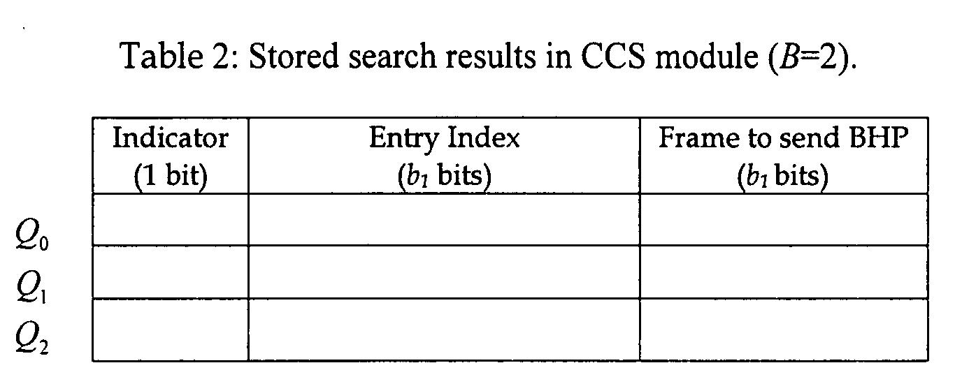
After comparing the indicator columns from the DCS and CCS modules, the
BHP processor 82 in Figure 3 knows whether the data burst and its BHP can be
scheduled for a given FDL delay Qi, 1 ≤ i ≤ B and determines which configuration
information will be sent to the path & channel selector 44 in Figure 12. The three
possible scenarios are, (1) the data burst can be scheduled without using FDL buffer,
(2) the data burst can be scheduled via using FDL buffer, and (3) the data burst
cannot be scheduled.
In the third case, the data burst and its BHP are simply discarded. In the first
case, the following information will be sent to the path & channel selector: incoming
DCG identifier, incoming data channel identifier, outgoing DCG identifier, outgoing
data channel identifier, data burst arrival time to the spatial switch, data burst
duration, FDL identifier 0 (i.e. Q 0). The path & channel selector 44 will immediately
send back an ACK after receiving the information. In the second case, the following
information will be sent to the path & channel selector:
- incoming DCG identifier,
- incoming data channel identifier,
- number of candidate FDL buffer x,
- for (i=1 to x do)
- outgoing DCG identifier,
- outgoing data channel identifier,
- FDL identifier i,
- data burst arrival time to the spatial switch,
- data burst duration.
In the second scenario, the path & channel selector 44 will search for an idle
buffer channel to carry the data burst. The RBIS module 142 is similar to the one
described in connection with Figure 12, except that now it has a PM and PG pair for
each group of channels with delay Qi, 1 ≤ i ≤ B. An example is shown in Figure 16 for
B=2, as an example. With one parallel search, the RBIS module will know whether
the data burst can be scheduled. When x=1, the RBIS module 142 performs parallel
search on (P M1 90a, PG1 92a) or (P M2 90b, P G2 92b), depending on which FDL buffer is
selected by the BHP processor 82. If an idle buffer channel is found, it will inform the
processor 140, which in turn sends an ACK to the BHP processor 82. When x=2, both
(PM1, PG1) and (PM2, PG2) will be searched. If two idle channels with different delays
are found, the channel with delay Q 1 is chosen. In this case, an ACK together with
the information that Q 1 is chosen will be sent to the BHP processor 82. After a
successful search, the RBIS module 142 will update the corresponding PM and PG
pair.
Figures 17 - 26 illustrate variations of the LAUC-VF method, cited above. In
the LAUC-VF method cited above, two associative processors PM and PG are used to
store the status of all channels of the same outbound link. Specifically, PM stores r
words, one for each of the r data channels of an outbound link. It is used to record
the unscheduled times of these channels. PG contains n superwords, one for an
available time interval (a gap) of some data channel. The times stored in PM and PG
are relative times. PM and PG support associative search operations, and data
movement operations for maintaining the times in a sorted order. Due to parallel
processing, PM and PG are used as major components to meet stringent real-time
channel scheduling requirement.
In the embodiment described in Figures 22-23, a pair of associative processors
PM and PG for the same outbound link are combined into one associative processor
PMG. The advantage of using a unified PMG to replace a pair of PM and PG is the
simplification of the overall core router implementation. In terms of ASIC
implementation, the development cost of a PMG can be much lower than that of a pair
of PM and PG. PMG can be used to implement a simpler variation of the LAUC-VF
method with faster performance.
In Figures 17a and 17b, two outbound channels Ch1 and Ch2 are shown, with t0
being the current time. With respect to t0, channel Ch1 has two DBs, DB1 and DB2,
scheduled and channel Ch2 has DB3 scheduled. The time between DB1 and DB2 on Ch1,
which is a maximal time interval that is not occupied by any DB, is called a gap. The
times labeled t1 and t2 are the unscheduled time for Ch1 and Ch2, respectively. After t1
and t2, Ch1 and Ch2 are available for transmitting any DB, respectively.
The LAUC-VF method tries to schedule DBs according to certain priorities.
For example, suppose that a new data burst DB4 arrives at time t'. For the situation of
Figure 17a, DB4 can be scheduled within the gap on Ch1, or on Ch2 after the
unscheduled time of Ch2. The LAUC-VF method selects Ch1 for DB4, and two gaps are
generated from one original gap. For the situation of Figure 17b, DB4 conflicts with
DB1 on Ch1 and conflicts with DB3 on Ch2. But by using FDL buffers, it may be
scheduled for transmission without conflicting DBs on Ch1 and/or DBs on Ch2.
Figure 17b shows the scheduling that DB4 is assigned to Ch2, and a new gap is
generated.
Assuming that an outbound link has r data channels, the status of this link can
be characterized by two sets:
In the embodiment of LAUC-VF proposed in U.S. Ser. No. 09/689,584, the two
associative processors PM and PG were proposed to represent SM and SG, respectively.
Due to fixed memory word length, the times stored in the associative memory M of
PM and the associative memory G of PG are relative times. Suppose the current time is
t0. Then any time value less than t0 is of no use for scheduling a new DB. Let
S'M = {(max{ti - t 0 , 0}, i )|(ti ,i) ∈ SM }
S'G = {(max{lj - t 0 , 0}, max{lj - t 0 , 0}, cj ) |(lj , rj , cj ) ∈ SG }
The times in S'M and S'G are times relative to the current time t0, which is used as a
reference point 0. Thus, M of PM and G of PG are actually used to store S'M and S'G
respectively.
The channel scheduler proposed in U.S. Ser. No. 09/689,584 assumes that DBs
have arbitrary lengths. One possibility is to assume a slot transmission mode. In this
mode, DBs are transmitted in units of slots, and BHPs are transmitted as groups, and
each group is carried by a slot. A slot clock CLKs is used to determine the slot
boundary. The slot transmissions are triggered by pulses of CLKs. Thus, the relative
time is represented in terms of number of CLKs cycles. The pulses of CLKs are shown
in Figure 18. In addition to clock CLKs, there is another finer clock CLKf. The period of
CLKs is a multiple of the period CLKf. In the example shown in Figures 18, one CLKs
cycle contains sixteen CLKf cycles. Clock CLKf is used to coordinate operations
performed within a period of CLKs.
In Figures 19a and 19b, modifications to the hardware design of PM and PG
given in U.S. Ser. No. 09/689,584 are provided for accommodation of slot
transmissions. In PM, there is an associative memory M of r words. Each word M; of
M is essentially a register, and it is associated with a subtractor 200. A register MC
holds an operand. In the embodiment of Figure 19a, the value stored in MC is the
elapsed time since the last update of M. The value stored in MC is broadcast to all
words Mi, 1 ≤ i ≤ r. Each word Mi does the following: Mj ← Mj - MC if Mj > MC;
otherwise, Mi←0. This operation is used to update the relative times stored in M. If
MC stores the elapsed time since last time parallel subtraction operation is
performed, performing this operation again updates these times to the time relative
to the time when this new PARALLEL-SUBTRACTION is performed. Another
operation is the parallel comparison. In this operation, the value stored in MC is
broadcast to all words Mi, 1 ≤ i ≤ r. Each word Mi does the following: if MC > Mi then
MFLAGi = 1, otherwise MFLAGi = 0. Signals MFLAGi, 1 ≤ i ≤ r, are transformed into
an address by a priority encoder. This address and the word with this address are
output to the address and data registers, respectively, of M. This operation is used to
find a channel for the transmission of a given DB. Similarly, two subtractors are used
for a word, one for each sub-word, of the associative memory G in PG.
An alternative design, shown in Figure 19b, is to implement each word Mi in
M as a decrement counter with parallel load. The counter is decremented by 1 by
every pulse of the system slot clock CLKs. The counting stops when the counter
reaches 0, and the counting resumes once the counter is set to a new positive value.
Suppose that at time t0 the counter's value is t' and at time ti > t0 the counters value is
t". Then t" is the same time of t', but relative to ti, i.e. t" = max{t' - (t1 - t0), 0}. Note
that any negative time (i.e. t' - (t1 - t0) < 0) with the new reference point t1 is not useful
in the lookahead channel scheduling. Associated with each word Mi is a comparator
204. It is used for the parallel comparison operation. Similarly, a word of G in PG can
be implemented by two decrement counters with two associated comparators.
The system has a c-bit circular increment counter Cs. The value of Cs is
incremented by 1 by every pulse of slot clock CLKs. Let tlatency (BHPi) be the time, in
terms of number of S'G cycles, between the time BHPi is received by the router and
the time BHPi is received by the channel scheduler. The value c is chosen such that:
 where MAXs is the number of CLKf cycles within a CLKs cycle. When BHPi is received
by the router, BHPi is timestamped by operations timestamprecv(BHPi) ← Cs. When
BHPi is received by the scheduler of the router, BHPi is timestamped again by
timestampsch(BHPi) ← Cs. Let
where MAXs is the number of CLKf cycles within a CLKs cycle. When BHPi is received
by the router, BHPi is timestamped by operations timestamprecv(BHPi) ← Cs. When
BHPi is received by the scheduler of the router, BHPi is timestamped again by
timestampsch(BHPi) ← Cs. Let
Di = (timestamprecv (BHPi ) + 2c - timestampsch (BHPi )) mod 2c .
Then, the relative arrival time (in terms of slot clock CLKs) of DBi at the optical
switching matrix of the router is Ti=Δ+τi+Di, where τ i is the offset time between BHPi
and DBi, and D is the fixed input FDL time. Using the slot time at which
timestampsch(BHPi) ← Cs is performed as reference point, and the relative times stored
in PM and PG, DBi can be correctly scheduled.
In the hardware implementation of LAUC-VF method, associative processors
PM and PG are used to store and process S'M and S'G, respectively. At any time, S'M =
{(ti, i) |1 ≤ i ≤ r} and S'G = {(lj, rj, cj) |lj ≥ 0}. A pair (ti , i) in S'M represents the
unscheduled time on channel Chi, and a triple (lj, rj, cj) in S'G represents a time gap
(interval) [lj, rj] on channel Chcj. The unscheduled time ti can be considered as a semi-infinite
gap (interval) [ti, ∞]. Thus, by including such semi-infinite gaps into S'G, S'M
is no longer needed.
More specifically, let S"M = {(ti , ∞, i) |(ti, i) ∈ S'M }, and define S'MG = S"M ∪
S'G. The basic idea of combining PM and PG is to build PMG by modifying PG so that
PMG is used to process S'MG. We present the architecture of associative processor PMG
for replacing PM and PG. PMG uses an associative memory MG to store pairs in S'M
and triples in S'G. As G in PG, each word of MG has two sub-words, with the first one
for lj and second one for rj when it is used to store (lj , rj, cj). When a word of MG is
used to store a pair (ti, i) of S'M, the first sub-word is used for ti, and the second is
left unused. The first r words are reserved for S'M, and the remaining words are
reserved for S'G. The first r words are maintained in non-increasing order of their
first sub-word. The remaining words are also maintained in non-increasing order of
their first subword. New operations for PMG are defined.
Below, the structures and operations of PM and PG are summarized, and the
structure and operations of PMG are defined. The differences between PMG include the
number of address registers used, the priority encoders, and operations supported. It
is shown that PMG can be used to implement the LAUC-VF method without any
slow-down, in comparison with the implementation using PM and PG.
The outbound data channel of a core router has r channels (wavelengths) for
data transmission. These channels are denoted by Ch1, Ch2, .., Chr. Let S = {ti |1 ≤ i ≤
r}, where ti is the unscheduled time for channel Chi. In other words, at any time after
ti, channel Chi is available for transmission. Given a time T', PM is an associative
processor for fast search of T" = min{ti | ti ≥ T'}, where T' is a given time. Suppose that
T" = tj, then channel Chj is considered as a candidate data channel for transmitting a
DB at time T'.
For purposes of illustration, the structures of PM and PG are shown in Figures
20 and 21 and PMG is shown in Figure 22.
An embodiment of PM 210 is shown in Figure 20. Associative processor PM
includes an associative memory M 212 of k words, M1, M2, ..., Mk, one for each
channel of the data channel group. Each word is associated with a simple subtraction
circuit for subtraction and compare operations. The words are also connected as a
linear array. Comparand register MC 214 holds the operand for comparison. MCH
216 is a memory of k words, MCH1, MCH2,..., MCHk, with MCHj corresponding to Mj.
The words are connected as a linear array, and they are used to hold the channel
numbers. MAR 1 218 and MAR 2 220 are address registers for holding addresses for
accessing M and MCH. MDR 222 and MCHR 224 are data registers used to access M
and MCHR along with the MARs.
Associative processor PM supports the following major operations that are
used in the efficient implementation of the LAUC-VF channel scheduling operations:
For RANDOM-READ, RANDOM-WRITE and SEGMENT-SHIFT-DOWN
operations, each pair (Mj, MCHj) is treated as a superword. The output of
PARALLEL-SEARCH consists r binary signals, MFLAGi, 1 ≤ i ≤ r. MFLAGi = 1 if and
only if Mi ≤ MC. There is a priority encoder with MFLAGi, 1 ≤ i ≤ r, as input, and it
produces an address j and this value is loaded into MAR1 when PARALLEL-SEARCH
operation is completed. RANDOM-READ, RANDOM-WRITE,
PARALLEL-SEARCH and SEGMENT-SHIFT-DOWN operations are used to
maintain the non-increasing order of values stored in M.
Figure 21 illustrates a block diagram of the associative processor P G 92. A PG
is used to store unused gaps of all channels of an outbound link of a core router. A
gap is represented by a pair (l, r) of integers, where l and r are the beginning and the
end of the gap, respectively. Associative processor PG includes associative memory G
93, comparand register GC 230, memory GCH 232, address register GAR 234, data
registers GDR 236 and GCHR 238 and working registers GR 1 240 and GR 2 242.
G is an associative memory of n words, G1, G2..., Gn, with each Gi consisting of
two sub-words Gi,1 and Gi,2. The words are connected as a linear array. GC holds a
word of two sub-words, GC1 and GC2. GCH is a memory of n words, GCH1, GCH2,...,
GCHn with GCHj corresponding to Gj. The words are connected as a linear array, and
they are used to hold the channel numbers. GAR is an address register used to hold
address for accessing G. GDR, and GCHR are data registers used to access M and
MCHR, together with GAR.
Associative processor PG supports the following major operations that are
used in the efficient implementation of the LAUC-VF channel scheduling operations:
In PG, a triple (Gi,1,Gi,2,GCHi ) corresponds to a gap with beginning time Gi,1 and
ending time Gi,2 on channel GCHi. For RANDOM-WRITE, PARALLEL-DOUBLE-COMPARAND-SEARCH,
PARALLEL-SINGLE-COMPARAND-SEARCH,
BIPARTITION-SHIFT-UP, and BIPARTITION-SHIFT-DOWN operations, each triple
(Gi,1,Gi,2,GCHi ) is treated as a superword. The output of PARALLEL-DOUBLE-COMPARAND-SEARCH
(resp. PARALLEL-SINGLE-COMPARAND-SEARCH)
operation consists n binary signals, GFLAGi, 1≤ i ≤ n, such that GFLAGi = 1 if and
only if Gi,1 ≥GC1 and Gi,2 ≤ GC2 (resp. Gi , 1 ≥ GC1 ). There is a priority encoder with
GFLAGi, 1≤i ≤ n, as input, and it produces an address j and this value is loaded into
GAR1 when the operation is completed. RANDOM-WRITE, PARALLEL-SINGLE-COMPARAND-SEARCH,
BIPARTITION-SHIFT-UP, and BIPARTITION-SHIFT-DOWN
operations maintain the non-increasing order of values stored in Gi,1s.
The operations of PM and PG are discussed in greater detail in U.S. Ser. No.
09/689,584.
Figure 22 illustrates a block diagram of a processor PMG , which combines the
functions of the PM and PG processors described above. PMG includes associative
memory MG 248, comparand register MGC 250, memory MGCH 252, address
registers MGAR 1 254a and MGAR 2 254b, and data registers MGDR 256 and MGCHR
258.
MG is an associative memory of m = r + n words, MG1 , MG2,...,MGm, with
each MGi consisting of two sub-words MGi,1 and MGi,2. The words are also connected
as a linear array. MGC is a comparand register that holds a word of two sub-words,
MGC1 and MGC2. MGC also holds a word of two sub-words, MGC1 and MGC2.
MGCH is a memory of m words, MGCH1,MGCH2 ,...,MGCHm with MGCHj
corresponding to MGj. The words are connected as a linear array, and they are used
to hold the channel numbers.
Associative processor PMG supports the following major operations:
As in PG, a triple (MGi,1 , MGi,2, MGCHi) may correspond to a gap with
beginning time MGi,1 and ending time MGi,2 on channel MGCHi. But in such a case, it
must be that i > r. If i ≤ r, then MGi,2 is immaterial, the pair (MGi,1, MGCHi) is
interpreted as the unscheduled time MGi,1 on channel MGCHi, and this pair
corresponds to a word in PM. For RANDOM-READ, RANDOM-WRITE,
PARALLEL-COMPOUND-SEARCH, BIPARTITION-SHIFT-UP and SEGMENT-SHIFT-DOWN
operations, each triple (MGi,1, MGi,2,..., MGCHi) is treated as a
superword. The first r superwords are used for storing the unscheduled times of r
outbound channels, and the last m - r superwords are used to store information about
gaps on all outbound channels.
The output of PARALLEL-COMPOUND-SEARCH operation consists of
binary signals MGFLAGi whose values are defined as follows: (i) if MGC2 = 0 and
MGi,1 ≥ MGC1 then MGFLAGi = 1; (ii) if MGC2 ≠0, i ≤ r, MGi,1 ≥ MGC1 then MGFLAGi
= 1; (iii) if MGC2 ≠ 0, i> r, MGi,1 ≥ MGC1 and MGi,2 ≤ MGC2 then MGFLAG1 = 1, or if
MGi,1 ≥ MGC1 and i ≤ r then MGFLAGi = 1; and (iv) otherwise, MGFLAGi = 0.
There are two encoders. The first one uses MGFLAGi, 1 ≤ i ≤ r, as its input, and
it produces an address in MGAR1 after a PARALLEL-COMPOUND-SEARCH
operation is performed if MGC2 ≠ 0. The second encoder uses MGFLAGi, r + 1 ≤ i ≤ m,
as its input. It produces an address in MGAR2 after a PARALLEL-COMPOUND-SEARCH
operation is performed if MGC2 ≠ 0. There is a selector with the output of
the two encoders as its input. If MGC2 = 0, the smallest non-zero address produced
by the two encoders, if such an address exists, Ys loaded into MGAR1 after a
PARALLEL-COMPOUND-SEARCH operation is performed; otherwise, MGAR1 is
set to 0 after a PARALLEL-COMPOUND-SEARCH operation is performed; If MGC2
≠ 0, the output of the selector is disabled.
RANDOM-READ, RANDOM-WRITE, PARALLEL-COMPOUND-SEARCH1,
BIPARTITION-SHIFT-UP and SEGMENT-SHIFT-DOWN operations are used to
maintain the non-increasing order of values stored in MGi,1 of the first m words, and
the non-increasing order of the values stored in MGi,1 of the last m - r words.
The operations of associative processors PM and PG can be carried out by
operations of PMG without any delay when they are used to implement LAUC-VF
channel scheduling method. We assume that PMG contains m = r + n superwords. In
Table 3 (resp. Table 4), the operations of PM (resp. PG) given in the left column are
carried out by operations of PMG given the right column. Instead of searching PM and
PG concurrently, using PMG, this step can be carried out by PARALLEL-COMPOUND-SEARCH
operation.
| Simulation of PM by PMG | |
| PM | PMG |
| RANDOM-READ | RANDOM-READ |
| RANDOM-WRITE | RANDOM-WRITE |
| PARALLEL-SEARCH | PARALLEL-COMPOUND-SEARCH |
| SEGMENT-SHIFT-DOWN | SEGMENT-SHIFT-DOWN (with_MGAR 2 = m) |
| Simulation of PG by PMG | |
| PG | PMG |
| RANDOM-WRITE | RANDOM-WRITE |
| PARALLEL-DOUBLE-COMPARAND-SEARCH | PARALLEL-COMPOUND-SEARCH |
| PARALLEL-SINGLE-COMPARAND-SEARCH | PARALLEL-COMPOUND-SEARCH (with MGC2 = 0) |
| BIPARTITE-SHIFT-UP | SEGMENT-SHIFT-UP (with MGAR2 = m) |
| BIPARTITE-SHIFT-DOWN | SEGMENT-SHIFT-DOWN (with MGAR2 = m -1) |
In the LAUC-VF method, fitting a given DB into a gap is preferred, even the
DB can be scheduled on another channel after its unscheduled time, as shown by the
example of Figures 17a-b. With separate PM and PG and performing search operations
on PM and PG simultaneously, this priority is justifiable. However, the overall circuit
for doing so may be considered too complex.
By combining PM and PG into one associative processor, simpler and faster
variations of this LAUC-VF methods are possible. An alternative embodiment is
shown in Figure 23. In this figure, processor P*MG 270 includes an array TYPE 272
with m bits, each bit being associated with a corresponding word in memory MG. If
TYPEi = 1 then MGi stores an item of S'M otherwise, MGi stores an item of S'G.
Further, register TYPER 274 is a one-bit register used to access TYPE, together with
MGAR1 and MGAR2.
Other differences between P*MG and PMG include the priority encoder used and
the operations supported. When a new DB is scheduled, MG is searched. The fitting
time interval found, regardless if it is a gap or a semi-infinite interval, will be used
for the new DB. Once the DB is scheduled, one more gap may be generated. As long
as there is sufficient space in MG, the new gap is stored in MG. When MG is full, an
item of S'G may be lost. But it is enforced that all items of S'M must be kept.
Let ts out(DBi) and te out(DBi) be the transmitting time of the first and last slot of
DBi at the output of the router, respectively. Then
ts out (DBi ) = Ti + Lj
and
te out (DBi ) = Ti + Lj + length(DBi ),
where Ti is the relative arrival time defined above, Lj is the FDL delay time selected
for DBi in the switching matrix and length(DB2) is the length of DBi in terms of
number of slots. Assume that there are q+1 FDLs L0, L1,..., Lq in the DB switching
matrix such that L0 = 0 < L1 <L2 <...< Lq-i <Lq. The new variation of LAUC-VF is
sketched as follows:

Once a DB is scheduled, MG is updated. When a gap is to be added into MG,
and TYPEm = 1, the new gap is ignored. This ensures that no item belonging to S'M is
lost.
Associative processor P*MG supports the following major operations:
In operation, The value of TYPE; indicates the type of information stored in
MGi. As in PG, a triple (MGi,1, MGi,2, MGCHi) may correspond to a gap with
beginning time MGi,1 and ending time MGi,2 on channel MGCHi. But in such a case, it
must be that TYPE; = 0. If TYPEi = 1, then MGi,2 is immaterial, the pair (MGi,1,
MGCHi) is interpreted as the unscheduled time MGi,1 on channel MGCHi, and this
pair corresponds to a word in PM. For RANDOM-READ, RANDOM-WRITE,
PARALLEL-COMPOUND-SEARCH, BIPARTITION-SHIFT-UP and SEGMENT-SHIFT-DOWN
operations, each quadruple (MGi,1, MGi,2, TYPE;, MGCHi) is treated as
a superword.
The output of PARALLEL-COMPOUND-SEARCH operation consists of
binary signals MGFLAGi whose values are defined as follows. If MGC2 ≠ 0, TYPE = 0,
Gi, 1 ≥ GC1 and Gi,2 ≤ GC2 then MGFLAGi =1. If MGC2 = 0 and Gi, 1 ≥ GC1 then MGFLAGi
= 1. Otherwise, MGFLAGi = 0. There is a priority encoders. If MGFLAGi, 1 ≤ i ≤ m, as
its input, and it produces an address in MGAR1 after a PARALLEL-COMPOUND-SEARCH
operation is performed.
RANDOM-READ, RANDOM-WRITE, PARALLEL-COMPOUND-SEARCH,
BIPARTITION-SHIFT-UP and SEGMENT-SHIFT-DOWN operations are used to
maintain the non-increasing order of values stored in MGi,1s.
Figure 24 illustrates the use of multiple associative processors for fast
scheduling. Channel scheduling for an OBS core router is very time critical, and
multiple associative processors (shown in Figure 24 as P*MG processors 270), which
are parallel processors, are proposed to implement scheduling methods. Suppose
that there are q + 1 FDLs L0 = 0, L1 , ..., Lq in the DB switching matrix such that L0 < L1
< ... < Lq . These FDLs are used, when necessary, to delay DBs and increase the
possibility that the DBs can be successfully scheduled. In the implementation of the
LAUC-VF method presented in U.S. Ser. No.09/689,584, the same pair of PM and PG
are searched repeatedly using different FDLs until a scheduling solution is found or
all FDLs are exhausted. The method CHANNEL-SCHEDULING described above
uses the same idea.
To speed up the scheduling, a scheduler 42 may use q + 1 PM /PG pairs, one for
each Li. At any time, all q + 1 Ms have the same content, all q + 1 MCHs have the same
content, all q + 1 Gs have the same content, and all q + 1 GCHs have the same content.
Then finding a scheduling solution for all different FDLs can be performed on these
PM /PG pairs simultaneously. At most one search result is used for a DB. All PM /PG
pairs are updated simultaneously by the same lock-step operations to ensure that
they store the same information. Similarly, one may use q + 1 PMGs or P*MGs to speed
up the scheduling.
In Figure 24, a multiple processor system 300 uses q + 1 P*MGs 270 implement
the method CHANNEL-SCHEDULING described above. Similarly, the LAUC-VF
method can be implemented using multiple PM /PG pairs, or multiple PMGs in a similar
way to achieve better performance. The multiple P*MGs 270 include q + 1 associative
memories MG0, MG1,..., MGq. Each MGj has m words MGj 1, MGj 2, ..., MGj m, with
each MGj i consisting of two sub-words MGj i,1 and MGj i,2. There are q + 1 comparand
registers MGC0, MGC1,..., MGCq. Each MGCj holds a word of two sub-words, MGCj 1
and MGCj 2. MGCHs: There are q + 1 associative memories MGCH0 , MGCH1 ,...,
MGCHq. Each MGCHj has m words, MGCHj 1, MGCHj 2,..., MGCHj m. The words in
MGCHi are connected as a linear array. There are q + 1 linear arrays TYPE0,
TYPE1,..., TYPEq, where TYPEj has m bits, TYPEj 1,TYPEj 2, ...TYPEj m. MGAR1, MGAR
are address registers used to hold address for accessing MG and MGCH. MGDR,
TYPER, MGCH are: data registers used to access MGs, TYPEs and MGCHR.
This multiple processor system 300 supports the following major operations:
A RANDOM-READ operation is performed on one copy of P*MG, i.e. MG0,
TYPE0, and MGCj. RANDOM-WRITE, PARALLEL-COMPOUND-SEARCH,
BIPARTITION-SHIFTUP and SEGMENT-SHIFT-DOWN operations are performed
on all copes of P*MG. For RANDOM-READ, RANDOM-WRITE, PARALLEL-COMPOUND-SEARCH,
BIPARTITION-SHIFT-UP and SEGMENT-SHIFT-DOWN
operations, each quadruple (MGi,1, MGi,2, TYPEi, MGCHi) is treated as a superword.
When a PARALLEL-COMPOUND-SEARCH operation is performed, the output of
all P*MG copies are the input of selectors. The output of one P*MG copy is selected.
The CHANNEL-SCHEDULING method may be implemented in the multiple
processor system as:

It may be desirable to be able to partition the r data channels into groups and
choose a particular group to schedule DBs. Such situations may occur in several
occasions. For example, one may want to test a particular channel. In such a
situation, the channel to be tested by itself forms a channel group, and all other
channels form another group. Then, channel scheduling is only performed on the 1-channel
group. Another occasions is that during the operation of the router, some
channels may fail to transmit DBs. Then, the channels of the same outbound link can
be partitioned into two groups, the group that contains all failed channels, and the
group that contains all normal channels, and only normal channels are to be selected
for transmitting DBs. Partitioning data channels also allows channel reservation,
which has applications in quality of services. Using reserved channel groups, virtual
circuits and virtual networks can be constructed.
To incorporate group partition feature into channel scheduling associative
processors, the basic idea is to associate a group identifier (or gid for short) with each
channel. For a link, all the channels share the same gid belong to the same group. The
gid of a channel is programmable; i.e. it can be changed dynamically according to
need. The gid for a DB can be derived from its BHP and/or some other local
information.
The design of PM and PG to PM-ext and PG-ext may be extended to incorporate
multiple channel groups, as shown in Figures 25 and 26, respectively. As shown in
Figure 25, associative processor P M-ext 290 includes M, MC, MCH, MAR1, MAR2,
MDR, MCHR, as described in connection with Figure 20. MCIDC 292 is a comparand
register that holds the gid for comparison. MGID 294 is a memory of r words, MGID1,
MGID2,..., MGIDr, with MGIDj corresponding to Mj and MCHj. The words are
connected as a linear array, and they are used to hold the channel group numbers.
MGIDDR 296 is a data register.
PM-ext is similar to PM with the addition of several components, and modifying
operations. The linear array MGID has r locations, MGID1, MGID2 ,..., MGIDr ; each is
used to store an integer gid. MGIDi is associated with Mi and MCHi, i.e. a triple (Mi,
MCHi, MGIDi) is treated as a superword. Comparand register MGIDC and data
register MGIDDR are added.
Associative processor PM-ext supports the following major operations that are
used in the efficient implementation of the LAUC-VF channel scheduling operations.
For RANDOM-READ, RANDOM-WRITE and SEGMENT-SHIFT-DOWN
operations, each triple (Mj, MCHj, MGIDj) is treated as a superword. The output of
PARALLEL-SEARCH1 consists r binary signals, MFLAGi, 1 ≤ i ≤ r. MFLAGi = 1 if and
only if MGIDi = MGIDC. There is a priority encoder with MFLAGi, 1 ≤ i ≤ r, as input,
and it produces an address j and this value is loaded into MAR1 when PARALLEL-SEARCH1
operation is completed. The output of PARALLEL-SEARCH2 consists r
binary signals, MFLAGi, 1 ≤ i ≤ r. MFLAGi = 1 if and only if Mi ≤ MC and MGIDi =
MGIDC. The same priority encoder used in PARALLEL-SEARCH 1 transforms
MFLAGi, 1 ≤ i ≤ r, into an address j and this value is loaded into MAR1 when
PARALLEL-SEARCH operation is completed. RANDOM-READ, RANDOM-WRITE,
PARALLEL-SEARCH2 and SEGMENT-SHIFT-DOWN operations are used to
maintain the non-increasing order of values stored in M.
Figure 26 illustrates a block diagram of PG-ext. PG-ext 300 includes
G,GC,GCH,GAR,GDR,GCHR, as described in connection with Figure 21. GGIDC 302
is a comparand register for holding the gid for comparision. GGID 304 is a memory
of r words, GGID1, GGID2,..., GGIDr, with GGIDj corresponding to Gj and GCHj. The
words are connected as a linear array, and they are used to hold the channel group
numbers. GGIDR 306 is a data register.
Similar to the architecture of PM-ext, a linear array GGID of n words, GGID1,
GGID2,..., GGIDn is added to PG. A quadruple (Gi,1, Gi,2, MCHi, GGIDi) is treated as a
superword.
Associative processor PG-ext supports the following major operations that are
used in the efficient implementation of the LAUC-VF channel scheduling operations.
A quadruple (Gi,1, Gi,2, GCHi, GGIDi) corresponds to a gap with beginning time
Gi,1 and ending time Gi,2 on channel CCHi, whose gid is in GGIDi. For RANDOM-WRITE,
PARALLEL-DOUBLE-COMPARAND-SEARCH, PARALLEL-SINGLE-COMPARAND-SEARCH,
BIPARTITION-SHIFT-UP, and BIPARTITION-SHIFT-DOWN
operations, each quadruple (Gi , 1 , Gi,2, GCHi, GGIDi) is treated as a superword.
The output of PARALLEL-DOUBLE-COMPARAND-SEARCH (resp.
PARALLEL-SINGLECOMPARAND-SEARCH) operation consists n binary signals,
GFLAGi, 1 ≤ i ≤ n, such that GFLAGi = 1 if and only if Gi,1 ≥ GC1 and Gi,2 ≤ GC2 (resp.
Gi,1 ≥ GC1), GGIDi =GGIDC. There is a priority encoder with GFLAGi, 1 ≤ i ≤ n, as
input, and it produces an address j and this value is loaded into GAR, when the
operation is completed. RANDOM-WRITE, PARALLEL-SINGLE-COMPARAND-SEARCH,
BIPARTITION-SHIFTUP, and BIPARTITION-SHIFT-DOWN operations to
maintain the non-increasing order of values stored in Gi,1s.
Changing the gid of a channel Chj from g1 to g2 is done as follows: find the
triple (Mi, MCHi, MGIDi) such that MCHi, = j and store i into MAR1 and (MDR,
MCHR, MGIDDR); MGIDDR ← g2, and write back (MDR, MCHR, MGIDDR) using
the address i in MAR1.
Given a DB', ts out(DB'), te out (DB'), and a gid g, the scheduling of DB' involves
searches in PM-ext and PG-ext. Searching in PM-ext is done as follows: find the smallest i
such that Mi < ts out(DB') and MGIDi = g. Searching in PG-ext is done as follows: find the
smallest i such that Gi,1 < ts out (DB'), Gi,2 > ts out (DB'), and MGIDi = g.
Similarly, associative processors PG-ext and PG*-ext can be constructed by
adding a gid comparand register MGGIDC, a memory MGGID of m words MGGID1,
MGGID2 ,,MGGIDm, and a data register MGGIDDR. PMG-ext is a combination of PM-
ext and PG-ext. The operations of PMG-ext can be easily derived from the operations of PM-
ext and PG-ext since the PM-ext items and the PG-ext items are separated. In P*MG-ext, the PM-
ext items and the PG-ext items are mixed. Since the MGi,1 values of these items are in
non-decreasing order, finding the PM-ext item corresponding channel Chi can be
carried out by finding the smallest j such that MGGID j = i.
Although the Detailed Description of the invention has been directed to
certain exemplary embodiments, various modifications of these embodiments, as
well as alternative embodiments, will be suggested to those skilled in the art. The
invention encompasses any modifications or alternative embodiments that fall within
the scope of the Claims.
Claims (23)
- An optical burst-switched router, comprising:an optical switch for routing optical information from an incoming optical transmission medium to one of a plurality of outgoing optical transmission media, each outgoing media able to transmit optical information over a plurality of channels;a delay buffer coupled to said optical switch for providing a plurality of different delays for delaying selected information between said incoming transmission medium and one of said outgoing optical transmission media;scheduling circuitry associated with each respective outgoing medium, comprising an associative processor for storing information on both unscheduled time for each channel on the respective outgoing medium and time gaps on each channel on the respective outgoing medium.
- The router of claim 1 wherein said incoming optical transmission medium and outgoing optical transmission media comprise optical fibers.
- The router of claim 1 wherein said scheduling circuitry includes an associative memory having a plurality of entries for storing a beginning value and an ending value for each instance of a time gap or unscheduled time.
- The router of claim 3 wherein each entry has a channel value indicating an associated channel on said respective outgoing optical transmission medium.
- The router of claim 3 wherein unscheduled time is stored in an entry as a beginning value indicative of the beginning of the unscheduled time and wherein the ending value is set to a predetermined value.
- The router of claim 3 and further comprising a linear array of memory cells, each cell associated with a respective entry in the associative memory, wherein each cell indicates whether the respective entry is associated with either a time gap or with unscheduled time.
- The router of claim 1 wherein said associative processor for each channel includes circuitry for searching through said entries of said associative memory.
- A method of routing optical information through an optical burst-switched router including an optical switch for routing optical information from an incoming optical transmission medium to one of a plurality of outgoing optical transmission media, each outgoing media able to transmit optical information over a plurality of channels, and a delay buffer coupled to said optical switch for providing a plurality of different delays for delaying selected information between said incoming transmission medium and one of said outgoing optical transmission media, comprising the steps of:for each respective outgoing optical transmission medium, storing information on both unscheduled time for each channel and time gaps on each channel in an associative memory; andsearching said associative memories for available periods to schedule an optical burst.
- The method of claim 8 wherein said incoming optical transmission medium and outgoing optical transmission media comprise optical fibers.
- The method of claim 8 wherein said storing step comprises the step of storing a beginning value and an ending value for each instance of a time gap or unscheduled time in an entry in said respective associative memory.
- The method of claim 10 and further comprising the step of associating a channel value indicating an associated channel on said respective outgoing optical transmission medium with each entry.
- The method of claim 10 wherein unscheduled time is stored in an entry as a beginning value indicative of the beginning of the unscheduled time and wherein the ending value is set to a predetermined value.
- The method of claim 10 and further comprising indicating whether each entry is associated with either a time gap or with unscheduled time.
- An optical burst-switched router, comprising:an optical switch for routing optical information from an incoming optical transmission medium to one of a plurality of outgoing optical transmission media, wherein each of the outgoing optical transmission media can transmit data over a plurality of channels;circuitry for assigning a group identifier to each channel;scheduling circuits each associated with a respective outgoing medium, each scheduling circuit comprising:one or more associative processors storing information indicative of times available for scheduling a data burst on said associated outgoing optical transmission medium; andcircuitry for controlling said one or more associative processors to find an available time on one of a plurality of channels associated with a predetermined group identifier.
- The router of claim 14 wherein said incoming optical transmission medium and said outgoing optical transmission media comprise optical fibers.
- The router of claim 14 wherein said one or more of said channels are assigned a group identifier to identify the channels being tested.
- The router of claim 14 wherein said one or more of said channels are assigned a group identifier to identify the channels as failed channels.
- The router of claim 14 wherein said one or more of said channels are assigned a group identifier to identify the channels as reserved channels.
- A method of routing information through an optical burst-switched router including an optical switch for routing optical information from an incoming optical transmission medium to one of a plurality of outgoing optical transmission media, wherein each of the outgoing optical transmission media can transmit data over a plurality of channels, comprising the steps of:assigning group identifiers for respective groups of one or more channels;scheduling data burst through said switch responsive to available time on one of a plurality of channels associated with a predetermined group identifier.
- The method of claim 19 wherein said incoming optical transmission medium and said outgoing optical transmission media comprise optical fibers.
- The method of claim 19 and further comprising the step of assigning a group identifier to a group of channels being tested.
- The method of claim 19 and further comprising the step of assigning a group identifier to a group of failed channels.
- The method of claim 19 and further comprising the step of assigning a group identifier to a group of reserved channels.
Applications Claiming Priority (4)
| Application Number | Priority Date | Filing Date | Title |
|---|---|---|---|
| US25788400P | 2000-12-22 | 2000-12-22 | |
| US25738200P | 2000-12-22 | 2000-12-22 | |
| US257382 | 2000-12-22 | ||
| US257884 | 2000-12-22 |
Publications (1)
| Publication Number | Publication Date |
|---|---|
| EP1217863A2 true EP1217863A2 (en) | 2002-06-26 |
Family
ID=26945926
Family Applications (1)
| Application Number | Title | Priority Date | Filing Date |
|---|---|---|---|
| EP01129348A Withdrawn EP1217863A2 (en) | 2000-12-22 | 2001-12-17 | Unified associative memory of data channel schedulers in an optical router |
Country Status (3)
| Country | Link |
|---|---|
| EP (1) | EP1217863A2 (en) |
| JP (1) | JP2002305542A (en) |
| CN (1) | CN1360413A (en) |
Cited By (2)
| Publication number | Priority date | Publication date | Assignee | Title |
|---|---|---|---|---|
| WO2008077322A1 (en) | 2006-12-26 | 2008-07-03 | Huawei Technologies Co., Ltd. | A network node and a buffer device and a scheduling method |
| CN116112144A (en) * | 2022-12-22 | 2023-05-12 | 四川九洲电器集团有限责任公司 | Self-adaptive delay compensation synchronous transmission method for signal level data of optical fiber network |
Families Citing this family (1)
| Publication number | Priority date | Publication date | Assignee | Title |
|---|---|---|---|---|
| KR102161055B1 (en) * | 2013-10-07 | 2020-09-29 | 삼성전자주식회사 | Method and Apparatus for instruction scheduling using software pipelining |
-
2001
- 2001-12-17 EP EP01129348A patent/EP1217863A2/en not_active Withdrawn
- 2001-12-19 JP JP2001385592A patent/JP2002305542A/en not_active Withdrawn
- 2001-12-21 CN CN01133872.5A patent/CN1360413A/en active Pending
Cited By (5)
| Publication number | Priority date | Publication date | Assignee | Title |
|---|---|---|---|---|
| WO2008077322A1 (en) | 2006-12-26 | 2008-07-03 | Huawei Technologies Co., Ltd. | A network node and a buffer device and a scheduling method |
| EP2083528A4 (en) * | 2006-12-26 | 2009-12-30 | Huawei Tech Co Ltd | NETWORK NODES AND BUFFER EQUIPMENT AND SCHEDULING METHOD |
| US8249449B2 (en) | 2006-12-26 | 2012-08-21 | Huawei Technologies Co., Ltd. | Network node, buffer device, and scheduling method |
| CN116112144A (en) * | 2022-12-22 | 2023-05-12 | 四川九洲电器集团有限责任公司 | Self-adaptive delay compensation synchronous transmission method for signal level data of optical fiber network |
| CN116112144B (en) * | 2022-12-22 | 2024-04-09 | 四川九洲电器集团有限责任公司 | Self-adaptive delay compensation synchronous transmission method for signal level data of optical fiber network |
Also Published As
| Publication number | Publication date |
|---|---|
| CN1360413A (en) | 2002-07-24 |
| JP2002305542A (en) | 2002-10-18 |
Similar Documents
| Publication | Publication Date | Title |
|---|---|---|
| US20020118419A1 (en) | Unified associative memory of data channel schedulers in an optical router | |
| EP1220563A2 (en) | Channel scheduling in optical routers | |
| Chlamtac et al. | Quadro-star: A high performance optical WDM star network | |
| US6721315B1 (en) | Control architecture in optical burst-switched networks | |
| Chen et al. | Optimal burst scheduling in optical burst switched networks | |
| Ramamirtham et al. | Time sliced optical burst switching | |
| US8774176B2 (en) | High-capacity data switch employing contention-free switch modules | |
| EP0471344B1 (en) | Traffic shaping method and circuit | |
| US6778536B1 (en) | Combined wavelength division multiplexing, time division multiplexing, and asynchronous packet switching with common time reference | |
| US20020054732A1 (en) | Optical burst scheduling using partitioned channel groups | |
| US7230952B2 (en) | Self-configuring distributed switch | |
| US8150264B2 (en) | Methods for non-wavelength-converting multi-lane optical switching | |
| US20020034183A1 (en) | Switching systems and methods of operation of switching systems | |
| US7567556B2 (en) | Circulating switch | |
| US20040141510A1 (en) | CAM based system and method for re-sequencing data packets | |
| WO2006130130A1 (en) | Scheduling method and system for optical burst switched networks | |
| CN1285103A (en) | Method and device for synchronizing dynamic cynchronous transfer mode in ring topology | |
| US6804255B1 (en) | Hardware implementation of channel scheduling algorithms for optical routers with FDL buffers | |
| EP1217862A2 (en) | Method and apparatus for synchronized slotted optical burst switching | |
| US20070110052A1 (en) | System and method for the static routing of data packet streams in an interconnect network | |
| US7257127B1 (en) | Method and apparatus for burst scheduling | |
| US7639678B2 (en) | Multimodal data switch | |
| JP2002305542A (en) | Unified associative memory of data channel scheduler in optical router | |
| US20100128734A1 (en) | Polyphase rotating-access switch | |
| Liu et al. | Optical burst switching: the next IT revolution worth multiple billions dollars? |
Legal Events
| Date | Code | Title | Description |
|---|---|---|---|
| PUAI | Public reference made under article 153(3) epc to a published international application that has entered the european phase |
Free format text: ORIGINAL CODE: 0009012 |
|
| AK | Designated contracting states |
Kind code of ref document: A2 Designated state(s): AT BE CH CY DE DK ES FI FR GB GR IE IT LI LU MC NL PT SE TR |
|
| AX | Request for extension of the european patent |
Free format text: AL;LT;LV;MK;RO;SI |
|
| STAA | Information on the status of an ep patent application or granted ep patent |
Free format text: STATUS: THE APPLICATION HAS BEEN WITHDRAWN |
|
| 18W | Application withdrawn |
Effective date: 20050514 |