EP1217759A2 - Spread spectrum transmission circuit - Google Patents
Spread spectrum transmission circuit Download PDFInfo
- Publication number
- EP1217759A2 EP1217759A2 EP01130226A EP01130226A EP1217759A2 EP 1217759 A2 EP1217759 A2 EP 1217759A2 EP 01130226 A EP01130226 A EP 01130226A EP 01130226 A EP01130226 A EP 01130226A EP 1217759 A2 EP1217759 A2 EP 1217759A2
- Authority
- EP
- European Patent Office
- Prior art keywords
- transmission
- gain
- data
- circuit
- channel data
- Prior art date
- Legal status (The legal status is an assumption and is not a legal conclusion. Google has not performed a legal analysis and makes no representation as to the accuracy of the status listed.)
- Granted
Links
Images




Classifications
-
- H—ELECTRICITY
- H04—ELECTRIC COMMUNICATION TECHNIQUE
- H04J—MULTIPLEX COMMUNICATION
- H04J13/00—Code division multiplex systems
-
- H—ELECTRICITY
- H04—ELECTRIC COMMUNICATION TECHNIQUE
- H04B—TRANSMISSION
- H04B1/00—Details of transmission systems, not covered by a single one of groups H04B3/00 - H04B13/00; Details of transmission systems not characterised by the medium used for transmission
- H04B1/69—Spread spectrum techniques
- H04B1/707—Spread spectrum techniques using direct sequence modulation
-
- H—ELECTRICITY
- H04—ELECTRIC COMMUNICATION TECHNIQUE
- H04B—TRANSMISSION
- H04B2201/00—Indexing scheme relating to details of transmission systems not covered by a single group of H04B3/00 - H04B13/00
- H04B2201/69—Orthogonal indexing scheme relating to spread spectrum techniques in general
- H04B2201/707—Orthogonal indexing scheme relating to spread spectrum techniques in general relating to direct sequence modulation
- H04B2201/70703—Orthogonal indexing scheme relating to spread spectrum techniques in general relating to direct sequence modulation using multiple or variable rates
-
- H—ELECTRICITY
- H04—ELECTRIC COMMUNICATION TECHNIQUE
- H04J—MULTIPLEX COMMUNICATION
- H04J13/00—Code division multiplex systems
- H04J13/0077—Multicode, e.g. multiple codes assigned to one user
Definitions
- a transmission circuit comprising at least a baseband circuit for generating and outputting transmission data constituted by at least one first channel data and one second channel data, spreading means for spreading the transmission data with a spreading code that differs for each transmission channel, multiplication means for respectively weighting amplitudes of the first and second channel data by using a combination of two gain factors determined by a transmission data rate, digital modulation means for digitally modulating the first and second channel data whose amplitudes are weighted by the multiplication means, a quadrature modulator for quadrature-modulating the first and second channel data digitally modulated by the digital modulation means and outputting the data as a transmission signal, and an antenna for emitting the transmission signal output from the quadrature modulator as a radio wave, wherein the transmission circuit further comprises amplification means for amplifying the transmission signal output from the quadrature modulator with a gain based on a control voltage, a transmission level circuit for determining a transmission power value of the second channel data
- the transmission circuit in the fourth to sixth aspects further comprises amplification means for amplifying the transmission signal output from the quadrature modulator with a gain based on a control voltage, a transmission level circuit for determining a transmission power value of the second channel data component, a first gain offset circuit for adding, to a transmission power value determined by the transmission level circuit, a first gain correction amount for controlling a gain of the amplification means to keep transmission power of the second channel data component at the antenna end constant regardless of the transmission data rate by using a combination of two gain factors determined by the transmission data rate, and outputting the transmission power value, and a voltage generating circuit for generating a voltage for controlling the gain of the amplification means, on the basis of the transmission power value output from the first gain offset circuit, wherein the antenna emits the transmission signal output from the quadrature modulator and amplified by the amplification means as a transmission signal.
- the S/N (Signal to Noise) ratio in the quadrature modulator can be made constant, and a deterioration in adjacent channel leakage power can be prevented.
- the transmission power of the second channel data component at the antenna end can be made constant regardless of the transmission data rate.
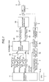
- the first embodiment is comprised of a baseband circuit 10 for generating and outputting two types of transmission data, namely data channel data DPDCH (Dedicated Physical Data Channel) serving as the first channel data and control channel data DPCCH (Dedicated Physical Control Channel) serving as the second channel data and also outputting gain factors ⁇ c, ⁇ d, ⁇ sc, and ⁇ sd serving as values for independently weighting I (Inphase) and Q (Quadrature) amplitudes in HPSK modulation and a TPC (Total Power Control) bit for controlling the transmission power of a terminal, a multiplier 20 serving as a spreading means for spreading the data channel data DPDCH output from the baseband circuit 10 by multiplying the data channel data DPDCH by a spreading code SCd, and outputting the resultant data as spread data d, a multiplier 22 serving as a spreading means for spreading the control channel data DPCCH output from the baseband circuit 10 by multiplying the control channel data DPCCH by a spreading code SCc, and out
- the digital signal Id output from the digital filter 40 is input to the digital/analog converter 41.
- the digital/analog converter 41 then converts the digital signal Id into the analog signal Ia and outputs it.
- the AGC amplifier control code output from the ⁇ offset circuit 3b is input to the voltage generating circuit 4.
- the voltage generating circuit 4 then generates a control voltage code for controlling the gain of the AGC amplifier 6 from the input AGC amplifier control code, and outputs the code.
- the data channel data DPDCH1 and DPDCH2 output from the baseband circuit 11 are respectively spread by a spreading code SCd1 and the spreading code SCd2 by a multiplier 20 and the multiplier 24.
- the multipliers 21 and 25 respectively multiply the spread data by the gain factor ⁇ sd.
- the synthesizing circuit 26 then synthesizes these two amplitude data and inputs the resultant data to the HPSK modulation circuit 30.
- Other operations are the same as those shown in Fig. 1.
Landscapes
- Engineering & Computer Science (AREA)
- Computer Networks & Wireless Communication (AREA)
- Signal Processing (AREA)
- Transmitters (AREA)
- Digital Transmission Methods That Use Modulated Carrier Waves (AREA)
Abstract
Description
Claims (12)
- A transmission circuit comprising a baseband circuit for generating and outputting at least one transmission data constituted by first and second channel data, spreading means for spreading the transmission data with a spreading code that differs for each transmission channel, multiplication means for respectively weighting amplitudes of the first and second channel data by using a combination of two gain factors determined by a transmission data rate, digital modulation means for digitally modulating the first and second channel data whose amplitudes are weighted by said multiplication means, a quadrature modulator for quadrature-modulating the first and second channel data digitally modulated by said digital modulation means and outputting the data as a transmission signal, and an antenna for emitting the transmission signal output from said quadrature modulator as a radio wave,
wherein said multiplication means weights the amplitudes of the first and second channel data by using gain factors that keep power of the transmission signal output from said quadrature modulator constant regardless of the transmission data rate without changing a ratio of a combination of gain factors determined by the transmission data rate. - A transmission circuit as claimed in claim 1, wherein said multiplication means weights the amplitudes of the first and second channel data by using gain factors determined on the basis of power of the transmission signal output from said quadrature modulator without changing a ratio of a combination of gain factors determined by the transmission data rate.
- A transmission circuit as claimed in claim 1, wherein said multiplication means weights the amplitudes of the first and second channel data by using gain factors that make a sum of a square of a gain factor for weighting the amplitude of the first channel data and a square of a gain factor for weighting the amplitude of the second channel data constant regardless of the transmission data rate without changing a ratio of a combination of gain factors determined by the transmission data rate.
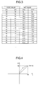
- A circuit as claimed in claim 1, 2 or 3 wherein said baseband circuit comprises a table storing a gain factor determined by the transmission data rate and a gain factor used by said multiplication means to weight the transmission data, and outputs a gain factor corresponding to the transmission data rate from said table to said multiplication means on the basis of the transmission data rate.
- A transmission circuit comprising a baseband circuit for generating and outputting at least one transmission data constituted by first and second channel data, spreading means for spreading the transmission data with a spreading code that differs for each transmission channel, multiplication means for respectively weighting amplitudes of the first and second channel data by using a combination of two gain factors determined by a transmission data rate, digital modulation means for digitally modulating the first and second channel data whose amplitudes are weighted by said multiplication means, a quadrature modulator for quadrature-modulating the first and second channel data digitally modulated by said digital modulation means and outputting the data as a transmission signal, and an antenna for emitting the transmission signal output from said quadrature modulator as a radio wave,
wherein said transmission circuit further comprises:wherein said antenna emits the transmission signal output from said quadrature modulator and amplified by said amplification means as a transmission signal.(a) amplification means for amplifying the transmission signal output from said quadrature modulator with a gain based on a control voltage;(b) a transmission level circuit for determining a transmission power value of the second channel data component;(c) a first gain offset circuit for adding, to a transmission power value determined by said transmission level circuit, a first gain correction amount for controlling a gain of said amplification means to keep transmission power of the second channel data component at the antenna end constant regardless of the transmission data rate by using a combination of two gain factors determined by the transmission data rate, and outputting the transmission power value; and(d) a voltage generating circuit for generating a voltage for controlling the gain of said amplification means, on the basis of the transmission power value output from said first gain offset circuit, and - A circuit as claimed in claim 4 or 5, wherein said transmission circuit further comprises:wherein said antenna emits the transmission signal output from said quadrature modulator and amplified by said amplification means as a transmission signal.(a) amplification means for amplifying the transmission signal output from said quadrature modulator with a gain based on a control voltage;(b) a transmission level circuit for determining a transmission power value of the second channel data component;(c) a first gain offset circuit for adding, to a transmission power value determined by said transmission level circuit, a first gain correction amount for controlling a gain of said amplification means to keep transmission power of the second channel data component at the antenna end constant regardless of the transmission data rate by using a combination of two gain factors determined by the transmission data rate, and outputting the transmission power value; and(d) a voltage generating circuit for generating a voltage for controlling the gain of said amplification means, on the basis of the transmission power value output from said first gain offset circuit, and
- A transmission circuit as claimed in claim 5 or 6, wherein said first gain offset circuit calculates transmission power of the first channel data component by using a combination of two gain factors determined by the transmission data rate, adds the transmission power as the first gain correction amount to the transmission power value determined by said transmission level circuit, and outputs the transmission power value.
- A transmission circuit as claimed in claim 5, 6 or 7 further comprising a second gain offset circuit for adding, to the transmission power value output from said first gain offset circuit, a second gain correction amount which is used to correct an output power error caused in said quadrature modulator when said multiplication means weights the amplitudes of the first and second channel data by using gain factors for weighting the amplitudes,
wherein said voltage generating circuit generates a voltage for controlling the gain of said amplification means, on the basis of the transmission power value output from said second gain offset circuit. - A transmission circuit as claimed in claim 8, wherein said second gain offset circuit calculates a ratio between output power of said quadrature modulator set when one combination of gain factors of gain factors used to weight the amplitudes of the first and second channel data by said multiplication means is set as a reference combination, and the reference combination of gain factors are used, and output power of said quadrature modulator set when gain factors used to weight the amplitudes of the first and second channel data by said multiplication means are used, adds the ratio as the second gain correction amount to the transmission power output from said first gain offset circuit, and outputs the transmission power.
- A transmission circuit as claimed in claim 9, wherein said second gain offset circuit includes a table storing a gain factor determined by the transmission data rate and a gain factor used by said multiplication means to weight the transmission data.
- A circuit as claimed in any one of claims 1 to 10, wherein the first channel data is data channel data of the transmission data, and
the second channel data is control channel data of the transmission data. - A circuit as claimed in any one of claims 1 to 11, wherein said digital modulation means is phase modulation means for phase shifting modulating amplitude data of the first and second channel data whose amplitudes are weighted by said multiplication means.
Applications Claiming Priority (2)
| Application Number | Priority Date | Filing Date | Title |
|---|---|---|---|
| JP2000387598A JP3956085B2 (en) | 2000-12-20 | 2000-12-20 | Transmitter circuit |
| JP2000387598 | 2000-12-20 |
Publications (3)
| Publication Number | Publication Date |
|---|---|
| EP1217759A2 true EP1217759A2 (en) | 2002-06-26 |
| EP1217759A3 EP1217759A3 (en) | 2004-04-07 |
| EP1217759B1 EP1217759B1 (en) | 2006-03-08 |
Family
ID=18854496
Family Applications (1)
| Application Number | Title | Priority Date | Filing Date |
|---|---|---|---|
| EP20010130226 Expired - Lifetime EP1217759B1 (en) | 2000-12-20 | 2001-12-19 | Spread spectrum transmission circuit |
Country Status (6)
| Country | Link |
|---|---|
| US (1) | US7023897B2 (en) |
| EP (1) | EP1217759B1 (en) |
| JP (1) | JP3956085B2 (en) |
| CN (1) | CN1205771C (en) |
| DE (1) | DE60117672T2 (en) |
| HK (1) | HK1048404B (en) |
Cited By (3)
| Publication number | Priority date | Publication date | Assignee | Title |
|---|---|---|---|---|
| EP1758257A4 (en) * | 2004-06-16 | 2007-07-04 | Mitsubishi Electric Corp | COMMUNICATION APPARATUS |
| WO2014016314A1 (en) | 2012-07-24 | 2014-01-30 | Centro Atlantico Del Medicamento S.A (Ceamed, S.A) | Fused quinonic compounds |
| EP2785117A4 (en) * | 2011-12-13 | 2015-01-28 | Huawei Tech Co Ltd | DOWNLINK SIGNAL PROCESSING DEVICE AND ITS PROCESSING METHOD |
Families Citing this family (29)
| Publication number | Priority date | Publication date | Assignee | Title |
|---|---|---|---|---|
| DE60211954T2 (en) * | 2002-01-29 | 2007-01-25 | Mitsubishi Denki K.K. | Transmission of an Additional Dedicated Physical Control Channel (ADPCCH) in a W-CDMA system |
| US8428181B2 (en) * | 2002-12-02 | 2013-04-23 | Research In Motion Limited | Method and apparatus for optimizing transmitter power efficiency |
| US7251462B2 (en) * | 2003-07-08 | 2007-07-31 | Matsushita Electric Industrial Co., Ltd. | Modulation circuit device, modulation method and radio communication device |
| JP4371830B2 (en) * | 2004-01-27 | 2009-11-25 | 富士通株式会社 | Distortion compensation amplifier and base station |
| KR100595652B1 (en) * | 2004-02-12 | 2006-07-03 | 엘지전자 주식회사 | Apparatus and method for controlling transmit power in mobile communication terminal |
| US7333563B2 (en) | 2004-02-20 | 2008-02-19 | Research In Motion Limited | Method and apparatus for improving power amplifier efficiency in wireless communication systems having high peak to average power ratios |
| JP4222957B2 (en) * | 2004-03-01 | 2009-02-12 | ソニー・エリクソン・モバイルコミュニケーションズ株式会社 | Transmission power control method and apparatus |
| JP4506310B2 (en) * | 2004-07-05 | 2010-07-21 | 富士通株式会社 | Up-transmission information identification code selection control circuit for W-CDMA communication terminal |
| US7359680B2 (en) * | 2004-09-14 | 2008-04-15 | Telefonaktiebolaget Lm Ericsson (Publ) | Delay calibration in polar modulation transmitters |
| US7376173B2 (en) * | 2004-09-27 | 2008-05-20 | Mitsubishi Electric Research Laboratories, Inc. | Unambiguously encoding and decoding signals for wireless channels |
| US7907671B2 (en) * | 2004-12-03 | 2011-03-15 | Motorola Mobility, Inc. | Method and system for scaling a multi-channel signal |
| CA2535189C (en) * | 2005-02-04 | 2011-04-12 | Samsung Electronics Co., Ltd. | Method and apparatus for setting gain factors for dedicated physical channels in a mobile telecommunications system |
| US8169890B2 (en) * | 2005-07-20 | 2012-05-01 | Qualcomm Incorporated | Systems and method for high data rate ultra wideband communication |
| EP1931056A4 (en) * | 2005-09-28 | 2014-04-23 | Nec Corp | Modulator, filter, filter gain control method, and code modulating method |
| US8761305B2 (en) | 2006-06-14 | 2014-06-24 | Blackberry Limited | Input drive control for switcher regulated power amplifier modules |
| CN100471085C (en) * | 2006-08-22 | 2009-03-18 | 华为技术有限公司 | Power control method and device for uplink physical channel |
| US8195217B2 (en) | 2006-08-22 | 2012-06-05 | Huawei Technologies Co., Ltd. | Method and apparatus for controlling power of uplink physical channel |
| JP5396874B2 (en) * | 2009-01-21 | 2014-01-22 | 日本電気株式会社 | Terminal device, transmission power control method, and digital signal processing device |
| FR2946206B1 (en) * | 2009-05-29 | 2015-02-27 | Alcatel Lucent | MULTI-FORMAT DATA TRANSMITTER |
| US8861627B2 (en) * | 2009-07-15 | 2014-10-14 | Fujitsu Limited | Direct mm-wave m-ary quadrature amplitude modulation (QAM) modulator operating in saturated power mode |
| CN102026350B (en) * | 2009-09-23 | 2014-08-13 | 中兴通讯股份有限公司 | Method and terminal for power regulation |
| US8903092B2 (en) * | 2010-06-04 | 2014-12-02 | Maxim Integrated Products, Inc. | High speed digital to analog converter with reduced spurious outputs |
| US8620238B2 (en) | 2010-07-23 | 2013-12-31 | Blackberry Limited | Method of power amplifier switching power control using post power amplifier power detection |
| WO2012064100A2 (en) * | 2010-11-09 | 2012-05-18 | 엘지전자 주식회사 | Method and terminal apparatus for transmitting a power status report in a wireless communication system |
| US9525444B2 (en) * | 2013-07-19 | 2016-12-20 | Analog Devices Global | Adaptive element shuffler |
| US11212141B2 (en) * | 2016-01-07 | 2021-12-28 | Qualcomm Incorporated | Methods and apparatus for a data transmission scheme for Narrow-Band Internet of Things (NB-IoT) |
| KR20200001147U (en) | 2018-11-26 | 2020-06-03 | 더인터맥스(주) | A Clothing with a Portable Property |
| CN110708268B (en) * | 2019-09-25 | 2021-08-27 | 维沃移动通信有限公司 | Signal modulation device and terminal |
| KR20200001459U (en) | 2020-06-25 | 2020-07-01 | 더인터맥스(주) | A Clothing with a Portable Property |
Family Cites Families (7)
| Publication number | Priority date | Publication date | Assignee | Title |
|---|---|---|---|---|
| JP3109589B2 (en) | 1998-03-18 | 2000-11-20 | 日本電気株式会社 | Method and apparatus for adjusting transmission power of CDMA terminal |
| JP4185601B2 (en) | 1998-10-30 | 2008-11-26 | 株式会社日立国際電気 | Transmission power control method, transmission power control apparatus, and base station including the same |
| US6904290B1 (en) | 1999-09-30 | 2005-06-07 | Telefonaktiebolaget L M Ericsson (Publ) | Method and apparatus for transmit power control |
| GB9923207D0 (en) | 1999-10-01 | 1999-12-08 | Lucent Technologies Inc | Power offset assignment for the physical control channel in universal mobile telecommunications systems (UMTS) |
| JP2002033629A (en) * | 2000-07-14 | 2002-01-31 | Nec Corp | Gain variable amplifier circuit, and terminal provided with the same |
| JP2002033716A (en) * | 2000-07-18 | 2002-01-31 | Sony Corp | CDMA spreading method and CDMA terminal device |
| ATE287142T1 (en) * | 2000-08-01 | 2005-01-15 | Ericsson Telefon Ab L M | AMPLITUDE LIMITATION |
-
2000
- 2000-12-20 JP JP2000387598A patent/JP3956085B2/en not_active Expired - Fee Related
-
2001
- 2001-12-18 US US10/020,186 patent/US7023897B2/en not_active Expired - Fee Related
- 2001-12-19 DE DE2001617672 patent/DE60117672T2/en not_active Expired - Lifetime
- 2001-12-19 EP EP20010130226 patent/EP1217759B1/en not_active Expired - Lifetime
- 2001-12-19 CN CNB011437537A patent/CN1205771C/en not_active Expired - Fee Related
-
2003
- 2003-01-15 HK HK03100381.4A patent/HK1048404B/en not_active IP Right Cessation
Cited By (6)
| Publication number | Priority date | Publication date | Assignee | Title |
|---|---|---|---|---|
| EP1758257A4 (en) * | 2004-06-16 | 2007-07-04 | Mitsubishi Electric Corp | COMMUNICATION APPARATUS |
| EP1783941A3 (en) * | 2004-06-16 | 2007-07-04 | Mitsubishi Denki Kabushiki Kaisha | Spread spectrum communication method and apparatus |
| US7519105B2 (en) | 2004-06-16 | 2009-04-14 | Mitsubishi Denki Kabushiki Kaisha | Channel code assignment according to gain factor |
| EP2785117A4 (en) * | 2011-12-13 | 2015-01-28 | Huawei Tech Co Ltd | DOWNLINK SIGNAL PROCESSING DEVICE AND ITS PROCESSING METHOD |
| US9609589B2 (en) | 2011-12-13 | 2017-03-28 | Huawei Technologies Co., Ltd. | Apparatus and method for processing downlink signal |
| WO2014016314A1 (en) | 2012-07-24 | 2014-01-30 | Centro Atlantico Del Medicamento S.A (Ceamed, S.A) | Fused quinonic compounds |
Also Published As
| Publication number | Publication date |
|---|---|
| HK1048404B (en) | 2005-11-25 |
| JP2002190840A (en) | 2002-07-05 |
| EP1217759B1 (en) | 2006-03-08 |
| US20020075943A1 (en) | 2002-06-20 |
| EP1217759A3 (en) | 2004-04-07 |
| CN1205771C (en) | 2005-06-08 |
| CN1360411A (en) | 2002-07-24 |
| HK1048404A1 (en) | 2003-03-28 |
| DE60117672D1 (en) | 2006-05-04 |
| US7023897B2 (en) | 2006-04-04 |
| JP3956085B2 (en) | 2007-08-08 |
| DE60117672T2 (en) | 2006-08-17 |
Similar Documents
| Publication | Publication Date | Title |
|---|---|---|
| EP1217759B1 (en) | Spread spectrum transmission circuit | |
| US7103029B1 (en) | Transmitter gain stabilizing apparatus | |
| US8064326B2 (en) | Mobile station, base station, communication system, and communication method | |
| KR101107866B1 (en) | Correlation Adaptive Precompensator | |
| EP1107449A2 (en) | Non-linear distortion compensation circuit, transmitter device to be employed in the same and mobile communication unit | |
| US7489907B2 (en) | Transmitter for suppressing a variation in input level of a multicarrier signal | |
| EP1137174A2 (en) | Automatic gain control system | |
| KR100303371B1 (en) | Radio transmitting apparatus and gain control method for the same | |
| KR20020009571A (en) | Decresting peaks in a cdma signal | |
| JP5131381B2 (en) | Method and apparatus for calculating transmission power control parameter | |
| EP1185016A1 (en) | Multiplex communication system and method of signal processing | |
| JP4492820B2 (en) | Transmitter circuit | |
| US7742516B2 (en) | Modulator | |
| JP4185601B2 (en) | Transmission power control method, transmission power control apparatus, and base station including the same | |
| JP2004007083A (en) | Transmission device | |
| KR100425705B1 (en) | Apparatus for measuring power of base band digital signal in transmission power auto gain control circuit | |
| JPH09116474A (en) | Wireless communication device | |
| JP2002026745A (en) | Wireless transmitter | |
| JP2003298358A (en) | Power amplifying device for wireless transmitter, program for controlling power amplifying device, and power amplifying method for wireless transmitter |
Legal Events
| Date | Code | Title | Description |
|---|---|---|---|
| PUAI | Public reference made under article 153(3) epc to a published international application that has entered the european phase |
Free format text: ORIGINAL CODE: 0009012 |
|
| AK | Designated contracting states |
Kind code of ref document: A2 Designated state(s): AT BE CH CY DE DK ES FI FR GB GR IE IT LI LU MC NL PT SE TR |
|
| AX | Request for extension of the european patent |
Free format text: AL;LT;LV;MK;RO;SI |
|
| PUAL | Search report despatched |
Free format text: ORIGINAL CODE: 0009013 |
|
| RIC1 | Information provided on ipc code assigned before grant |
Ipc: 7H 04B 7/005 B Ipc: 7H 04B 1/707 A |
|
| AK | Designated contracting states |
Kind code of ref document: A3 Designated state(s): AT BE CH CY DE DK ES FI FR GB GR IE IT LI LU MC NL PT SE TR |
|
| AX | Request for extension of the european patent |
Extension state: AL LT LV MK RO SI |
|
| 17P | Request for examination filed |
Effective date: 20040226 |
|
| 17Q | First examination report despatched |
Effective date: 20040708 |
|
| AKX | Designation fees paid |
Designated state(s): DE FR GB IT |
|
| GRAP | Despatch of communication of intention to grant a patent |
Free format text: ORIGINAL CODE: EPIDOSNIGR1 |
|
| GRAS | Grant fee paid |
Free format text: ORIGINAL CODE: EPIDOSNIGR3 |
|
| GRAA | (expected) grant |
Free format text: ORIGINAL CODE: 0009210 |
|
| AK | Designated contracting states |
Kind code of ref document: B1 Designated state(s): DE FR GB IT |
|
| REG | Reference to a national code |
Ref country code: GB Ref legal event code: FG4D |
|
| REF | Corresponds to: |
Ref document number: 60117672 Country of ref document: DE Date of ref document: 20060504 Kind code of ref document: P |
|
| ET | Fr: translation filed | ||
| PLBE | No opposition filed within time limit |
Free format text: ORIGINAL CODE: 0009261 |
|
| STAA | Information on the status of an ep patent application or granted ep patent |
Free format text: STATUS: NO OPPOSITION FILED WITHIN TIME LIMIT |
|
| 26N | No opposition filed |
Effective date: 20061211 |
|
| REG | Reference to a national code |
Ref country code: GB Ref legal event code: 732E Free format text: REGISTERED BETWEEN 20141023 AND 20141029 |
|
| REG | Reference to a national code |
Ref country code: FR Ref legal event code: TP Owner name: LENOVO INNOVATIONS LIMITED (HONG KONG), HK Effective date: 20141119 |
|
| PGFP | Annual fee paid to national office [announced via postgrant information from national office to epo] |
Ref country code: FR Payment date: 20141208 Year of fee payment: 14 |
|
| PGFP | Annual fee paid to national office [announced via postgrant information from national office to epo] |
Ref country code: IT Payment date: 20141203 Year of fee payment: 14 |
|
| REG | Reference to a national code |
Ref country code: FR Ref legal event code: ST Effective date: 20160831 |
|
| PG25 | Lapsed in a contracting state [announced via postgrant information from national office to epo] |
Ref country code: FR Free format text: LAPSE BECAUSE OF NON-PAYMENT OF DUE FEES Effective date: 20151231 |
|
| PG25 | Lapsed in a contracting state [announced via postgrant information from national office to epo] |
Ref country code: IT Free format text: LAPSE BECAUSE OF NON-PAYMENT OF DUE FEES Effective date: 20151219 |
|
| PGFP | Annual fee paid to national office [announced via postgrant information from national office to epo] |
Ref country code: GB Payment date: 20161214 Year of fee payment: 16 Ref country code: DE Payment date: 20161213 Year of fee payment: 16 |
|
| REG | Reference to a national code |
Ref country code: DE Ref legal event code: R119 Ref document number: 60117672 Country of ref document: DE |
|
| GBPC | Gb: european patent ceased through non-payment of renewal fee |
Effective date: 20171219 |
|
| PG25 | Lapsed in a contracting state [announced via postgrant information from national office to epo] |
Ref country code: DE Free format text: LAPSE BECAUSE OF NON-PAYMENT OF DUE FEES Effective date: 20180703 |
|
| PG25 | Lapsed in a contracting state [announced via postgrant information from national office to epo] |
Ref country code: GB Free format text: LAPSE BECAUSE OF NON-PAYMENT OF DUE FEES Effective date: 20171219 |