EP1217524A2 - Method and system for data block sparing in a solid-state storage device - Google Patents
Method and system for data block sparing in a solid-state storage device Download PDFInfo
- Publication number
- EP1217524A2 EP1217524A2 EP01310297A EP01310297A EP1217524A2 EP 1217524 A2 EP1217524 A2 EP 1217524A2 EP 01310297 A EP01310297 A EP 01310297A EP 01310297 A EP01310297 A EP 01310297A EP 1217524 A2 EP1217524 A2 EP 1217524A2
- Authority
- EP
- European Patent Office
- Prior art keywords
- spare
- page
- data block
- address
- region
- Prior art date
- Legal status (The legal status is an assumption and is not a legal conclusion. Google has not performed a legal analysis and makes no representation as to the accuracy of the status listed.)
- Withdrawn
Links
Images

Classifications
-
- G—PHYSICS
- G06—COMPUTING OR CALCULATING; COUNTING
- G06F—ELECTRIC DIGITAL DATA PROCESSING
- G06F12/00—Accessing, addressing or allocating within memory systems or architectures
- G06F12/02—Addressing or allocation; Relocation
- G06F12/08—Addressing or allocation; Relocation in hierarchically structured memory systems, e.g. virtual memory systems
- G06F12/10—Address translation
-
- G—PHYSICS
- G06—COMPUTING OR CALCULATING; COUNTING
- G06F—ELECTRIC DIGITAL DATA PROCESSING
- G06F3/00—Input arrangements for transferring data to be processed into a form capable of being handled by the computer; Output arrangements for transferring data from processing unit to output unit, e.g. interface arrangements
- G06F3/06—Digital input from, or digital output to, record carriers, e.g. RAID, emulated record carriers or networked record carriers
- G06F3/0601—Interfaces specially adapted for storage systems
- G06F3/0602—Interfaces specially adapted for storage systems specifically adapted to achieve a particular effect
- G06F3/0614—Improving the reliability of storage systems
- G06F3/0616—Improving the reliability of storage systems in relation to life time, e.g. increasing Mean Time Between Failures [MTBF]
-
- G—PHYSICS
- G06—COMPUTING OR CALCULATING; COUNTING
- G06F—ELECTRIC DIGITAL DATA PROCESSING
- G06F3/00—Input arrangements for transferring data to be processed into a form capable of being handled by the computer; Output arrangements for transferring data from processing unit to output unit, e.g. interface arrangements
- G06F3/06—Digital input from, or digital output to, record carriers, e.g. RAID, emulated record carriers or networked record carriers
- G06F3/0601—Interfaces specially adapted for storage systems
- G06F3/0628—Interfaces specially adapted for storage systems making use of a particular technique
- G06F3/0638—Organizing or formatting or addressing of data
- G06F3/064—Management of blocks
-
- G—PHYSICS
- G06—COMPUTING OR CALCULATING; COUNTING
- G06F—ELECTRIC DIGITAL DATA PROCESSING
- G06F3/00—Input arrangements for transferring data to be processed into a form capable of being handled by the computer; Output arrangements for transferring data from processing unit to output unit, e.g. interface arrangements
- G06F3/06—Digital input from, or digital output to, record carriers, e.g. RAID, emulated record carriers or networked record carriers
- G06F3/0601—Interfaces specially adapted for storage systems
- G06F3/0668—Interfaces specially adapted for storage systems adopting a particular infrastructure
- G06F3/0671—In-line storage system
- G06F3/0673—Single storage device
- G06F3/0679—Non-volatile semiconductor memory device, e.g. flash memory, one time programmable memory [OTP]
Definitions
- Magnetic disk drives provide inexpensive, non-volatile storage of large amounts of electronic data, high rates of data transfer, and high reliability over large numbers of read and write cycles. For these reasons, magnetic disk drives are the predominant mass storage devices in current computer systems. As with any physical material, the surfaces of rotating magnetic media are subject to manufacturing defects and defects that arise during use due to mechanically and electrically induced stresses. In order to enhance the reliability of magnetic media, sophisticated defect-circumventing mechanisms have been developed to map defective data storage regions of a magnetic medium to available, unused, spare data storage regions provided on the magnetic medium. A variety of methods for remapping defective areas have been developed and are currently in use. Most depend on provision of extensive lookup tables that are interspersed with data-containing regions of the magnetic medium.
- solid-state storage devices With the continuing decrease in cost, and increase in capacity, of integrated-circuit electronic memory devices, solid-state, storage devices have become an increasingly fast data storage and data retrieval characteristics of electronic memory are needed. In such applications, the higher data transfer rates of solid-state storage devices with respect to magnetic disk drives may offset and justify the higher cost, per data unit stored, of solid-state storage devices versus magnetic disk drives.
- magnet disk drives Just as regions of the surfaces of magnet disk drives may contain manufacturing defects, or may become defective through use, data-storage cells within an electronic memory may be defective upon manufacture or may fail during use.
- solid-state storage devices need to provide enhanced overall reliability by detecting defective memory cells and providing spare memory cells as substitutes for defective memory cells.
- magnetic data storage medium is relatively cheap, so that use of a relatively large fraction of the physical data storage medium for remapping tables in magnetic disk drives does not significantly increase the overall cost of a magnetic disk drive.
- complex remapping calculations may be undertaken in magnetic disk drives without significantly increasing access times and decreasing data transfer rates.
- solid-state storage devices by contrast, the physical storage medium is expensive, and therefore the use of a relatively large fraction of the medium for remapping tables can significantly increase the overall price of a solid-state storage device and significantly decrease the solid-state storage device's cost effectiveness in a given application, and complex remapping calculations directly increase access times and decrease data transfer rates.
- designers, manufacturers, and users of solid-state storage devices have recognized the need for a method and system for dynamically substituting spare memory cells to replace defective memory cells in the solid-state storage device that does not employ large remapping tables and complex remapping calculations.
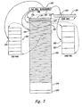
- a data block comprising a fixed number of bytes, is addressed in the solid-state storage device by a logical data block address formed by the concatenation of a page index and a data block index.
- the page index selects a particular spare table from the low-address and high-address spare table regions, a particular spare page within the low-address and high-address spare page regions, and a particular data page within the data page region.
- the data block index portion of the logical data block address selects a particular element from a spare table, a particular data block from a spare page, and a particular data block from a data page.
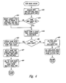
- a logical data block address is resolved by the solid-state data storage device into a physical data block address by first checking the status of a spare table element associated with the logical data block address to determine whether or not the logical data block address has been remapped. If the logical data block has been remapped, offset information in the spare table, along with the page index and data block address, are used to select the physical address of a spare data block within a spare page. If the status information within the spare table associated with a logical data block address indicates that the logical data block address is not remapped, then the page index and data block index components of the logical data block address are used to select the physical address of a data block within a data page. In either case, the selected physical address is the address of the data block within the solid-state data storage device corresponding to the logical data block address.
- the present invention provides a method and system for addressing data blocks within a solid-state data storage device that additionally provides space-efficient and computationally efficient bad data block replacement.
- a detailed C++-like pseudocode implementation of a specific embodiment of the present invention is provided.
- C++-like pseudocode is chosen for conciseness of description and for its broad use and acceptability in the engineering community.
- the present invention may most commonly be implemented directly in hardware circuits or in firmware. Such implementations are specified in relatively high-level specification languages that are compiled either to integrated circuits or to firmware instructions.
- Figure 1 illustrates physical addressing of data storage units within a solid-state data storage device.
- a convenient fundamental data storage unit widely used in the computer industry is called a "byte," a physical representation of an unsigned integer with a value ranging from 0 to 255, stored in eight binary digits, or bits.
- the bytes composing electronic memory are uniquely addressable. The entire electronic memory may be thought of as a very long, linear sequence of bytes starting from an initial byte with address 0 and ending with a final byte having an address equal to the total number of bytes in the memory minus one.
- the present invention will be describe in terms of a byte-addressable electronic memory, the present invention is equally applicable to electronic memories using different basic units of data storage, for example, 32-bit integers or 64-bit integers, and is applicable to electronic memories employing more complex addressing mechanisms.
- the physical addresses can be transformed into virtual physical addresses for a virtual sequential ordering of discretely addressed data storage entities.
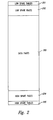
- the solid-state storage device selects a spare page from either the low-address spare page region 202 or the high-address spare page region 204.
- the status extracted from the spare table element 306 indicates from which spare page region to select the spare page.
- the solid-state storage device uses the extracted page index as an offset into the appropriate spare pages region to select the spare page 307 that contains the spare data block corresponding to the LDBA.
- the solid-state storage device uses the offset extracted from the spare table element 306 in step 406 as a block offset within the spare page 307 to locate the physical block 308 corresponding to the LDBA.
- the solid-state storage device uses the extracted page index 304 as an offset into the data page region 203 to locate the data page 309 corresponding to the LDBA.
- the solid-state storage device uses the data-block index 303 as an offset into the data page 309 to identify the physical data block 310 associated with the LDBA.
- the following type definition and constant declarations are the fundamental parameters for the embodiment:
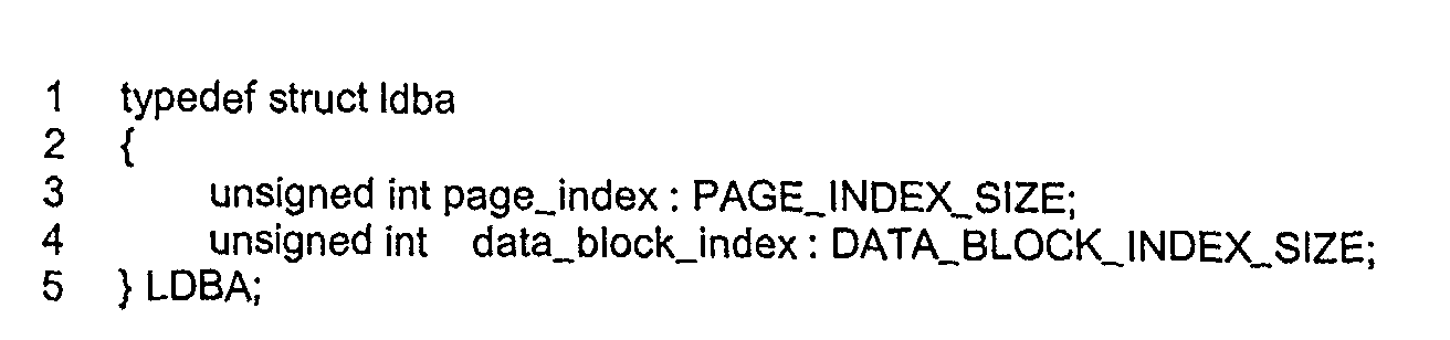
- the following type definition defines a structure representing an LDBA, including a page-index field and a data-block-index field:
- the status field can indicate whether or not an LDBA has been remapped and, if so, to which spare page region the LDBA has been remapped.
- the entire value of the spare status element considered as a byte may indicate whether or not a corresponding LDBA has been remapped, and a single bit may indicate to which spare page region the LDBA has been remapped.
- a portion of the first block in each spare page is dedicated as a spare block status map, the map comprising a number of bytes equal to the total number of blocks within the spare block page.
- Each byte of the spare status map may have one of the following values: The value "SPARES_STATUS_AVAILABLE,” declared on line 1, indicates that the corresponding block within the spare page is available for use to remap a data block. The value "SPARES_STATUS_IN_USE,” declared above on line 2, indicates that the corresponding block within the spare page is already being used to remap a data block, and the value "SPARES_STATUS_BAD,” declared on line 4, indicates that the corresponding block within the spare page is defective and unusable.
- the constant "RETRIES,” declared on line 1 is the number of times that a block access will be retried before the block is considered bad and remapping of the block is undertaken.
- the enumeration "status,” declared on line 2 is a return status for read-block and write-block operations undertaken by the memory device.
- the type definition on line 3 declares a "BYTE_PTR" to be a pointer to a byte.
- the class "MEMORY,” provided below, represents in C++-like pseudocode implementation of a solid-state storage device employing one embodiment of the present invention:
- the class “memory” includes the following four private data members: (1) “mem,” declared on line 4, a byte array representing the entire electronic memory; (2) “spareTab,” declared on line 5, an array of bytes that represents high-speed local memory storing a current spare table; (3) “lastUsedPageRegister,” declare on line 6, an integer representing a device register storing the page index corresponding to the spare table stored in spareTab; and (4) "spareUpdate,” a Boolean flag indicating whether or not the contents of spareTab have been altered since they were retrieved from memory.
- the class "memory” contains the following four public member functions, the first two of which define a read block and write block interface used by computers and other electronic devices to interface with the memory: (1) “readBlock,” declared above on line 23, that reads a block of data described by the supplied LDBA "address” into the supplied buffer “buff;” (2) “writeBlock,” declared above on line 24, that writes a block of data to the supplied LDBA "address” from the supplied buffer "buff;” (3) “memory,” a constructor that initializes the memory; and (4) " ⁇ memory,” declared on line 16, a member function that is called prior to shut down of the memory.
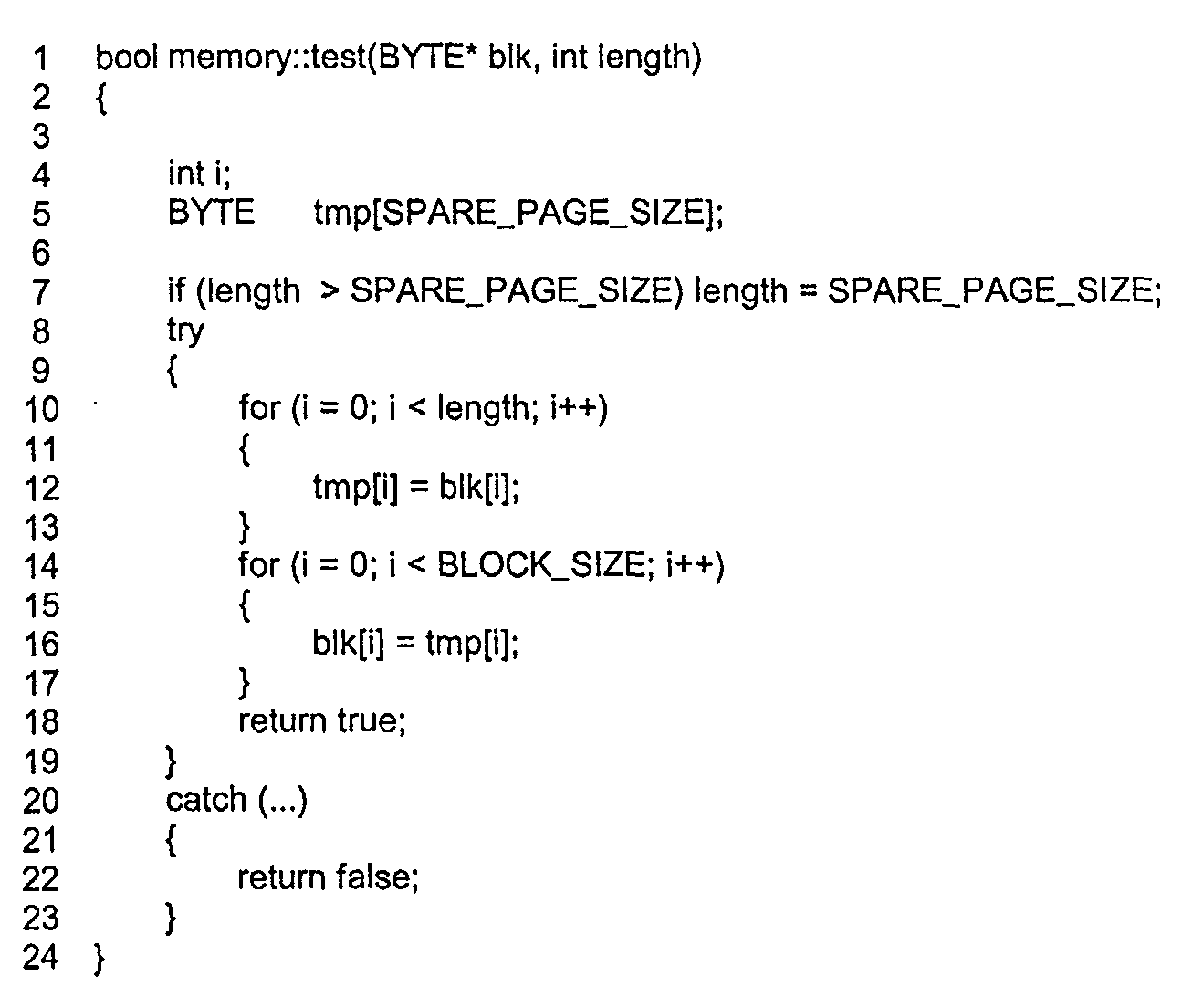
- This member function attempts to read the set of sequential bytes described by the arguments "block” and “length” into a temporary memory, on lines 10-13, and then write the contents of the temporary memory back to memory on lines 14-17. If an error occurs, then the Boolean value "false” is returned on line 22. Otherwise, the Boolean value "true” is returned on line 18.
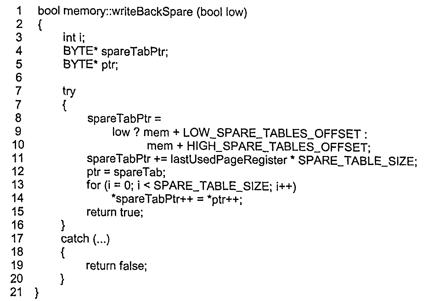
- the memory member function "writeBackSpare” is provided below:
- the member function “writeBackSpare” writes the contents of the data member "spareTab” back into memory at the appropriate position within either the low-address spare table region (201 in Figure 2) or the high-address spare table region (205 in Figure 2) depending on the value of argument "low.”
- the variable "spareTabPtr” is set to the address of the first byte of either the low-address spare table region or the high-address spare table region, depending on the value of argument "low.”
- an offset to the spare table corresponding to the page index currently stored in member "lastUsedPageRegister” is calculated and added to the value of local variable "spareTabPtr.”
- the contents of member "spareTab,” representing high-speed local memory for storing the spare table corresponding to the page index in lastUsedPageRegiste,r are written back to memory
- the memory member function "spareTable” is provided below:
- the member function "spareTable” loads, if necessary, a spare table corresponding to the page index "pageIndex" into data member “spareTab” that represents high-speed local memory.
- spareTable compares the supplied page index to the value stored in member "lastUsedPageRegister.” If the two values are equal, then the currently loaded spare table is the spare table corresponding to the supplied page index, no further actions are required, and a Boolean value "true” is returned. Otherwise, a spare table needs to be loaded from memory.
- spareTable attempts to load the spare table corresponding to the supplied page index into member "spareTab."
- SpareTable first attempts to load the spare table from the low-address spare table region on lines 20-26. If that fails, then spareTab attempts to load the spare table from the high-address memory region on lines 35-40. If that second attempt fails, then spareTab returns the value "false” on line 46. If a spare table is successfully copied from memory to member "spareTab,” then the member "lastUsedPageRegister" is updated, on lines 26 or 40, to contain the page index to which the spare table corresponds.
- Memory member function "dataBlock” is provided below: Member function “dataBlock” represents the LDBA-to-physical-address translation carried out by a solid-state storage device and illustrated in the flow-control diagram of Figure 4. The contents of the byte pointer "m” are updated by member function "dataBlock” to point to the first byte of a data block described by the supplied LDBA "address.” On line 7, dataBlock calls member function "spareTable” to load, if necessary, the spare table corresponding to the page index extracted from LDBA "address.” If a spare table cannot be loaded, then dataBlock returns the Boolean value "false” on line 7.
- dataBlock sets the local variable "sptb” to point to the spare table element corresponding to the data block described by the supplied LDBA "address.”
- dataBlock retrieves the status field from the spare table element pointed to by local variable "sptb” into local variable "status.” If the status is non-zero, as detected by dataBlock on line 11, then the LDBA "address" has been remapped.
- dataBlock sets the local variable "sparePagePtr" to the address of the spare block from the spare page corresponding to LDBA "address" on either line 14 or line 17, depending on whether the spare page resides in the low-address spare page region (202 in Figure 2) or the high-address spare page region (204 in Figure 2).
- badBlock remaps the LDBA supplied as argument "address.”
- badBlock calls member function "spareTable” to ensure that the currently loaded spare table corresponds to LDBA "address.”
- badBlock sets the local variable "sptb” to point to the spare table element corresponding to LDBA "address.”
- badBlock sets local variable "status” to the value of the status field of the error table element pointed to by variable "sptb.” If the status has a non-zero value, as detected on line 14, then the LDBA "address” has been previously remapped, and the previously remapped LDBA "address” is again remapped on lines 16-52.
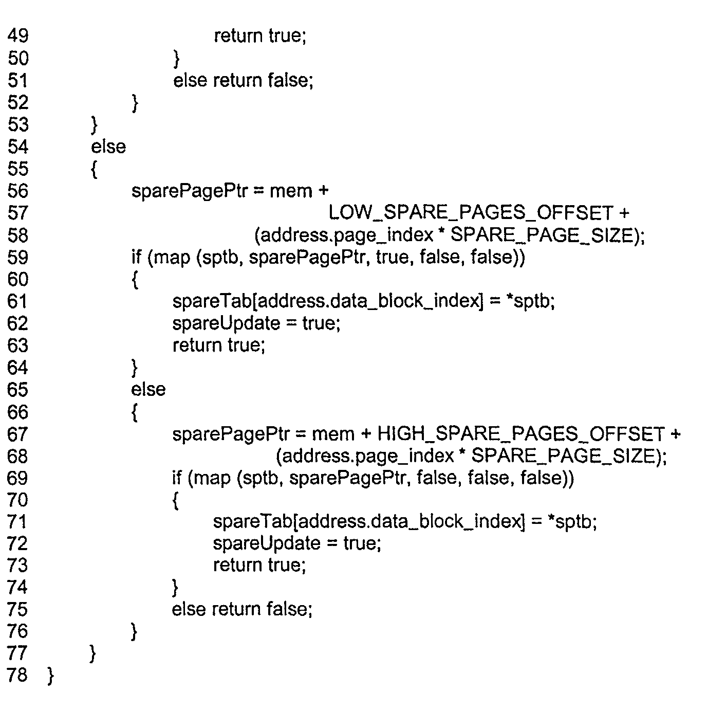
- the memory member function "map” is provided below: Member function "map” attempts to find an available spare block within the spare page for mapping an LDBA. Member function "map” is supplied with a pointer to a spare table element, a pointer to a spare page, and three Boolean arguments that indicate whether the spare page is in the low-address or high-address spare page regions, whether the spare page at the offset indicated by the spare table element should be designated as a bad spare block, and whether the available spare block should be tested prior to remapping. On line 12, local variable “ssmePtr” is set to point to the spare block status map that occupies the initial portion of the first block within the spare page.
- the spare status map is read from memory into variable "ssme.”
- the spare block status map is updated to indicate that the spare block referred to by the offset field of the spare table element pointed to by variable "sptb" is bad if the supplied argument "remap" has a Boolean value "true.”
- map searches the spare block status map in local variable "ssme” for an available spare block. If an available spare block is found, on line 18, then the spare block status map is updated on line 25, copied back to the spare page on lines 26-27, and the spare table element pointed to by variable "sptb" is updated to reflect the spare block within the spare page to which an LDBA has been remapped.
- Member function "writeBlock” is similar to member function "readBlock,” described above. However, in the case of member function "writeBlock,” if the block described by supplied LDBA "address" cannot be successfully written in the for -loop of lines 6-20, and if remapping of the block can be successfully completed, as detected by writeBlock on line 21, then the write operation is retried on lines 25-27. If writing to the remapped block is successful, then writeBlock returns status "OK" on line 32.
- a different spare page can be selected in which to find a replacement block.
- the described write block operation retries a failed write after successful remapping, but, in an alternate embodiment, a second attempt at the write may instead be the responsibility of an accessing device.
- Many other similar alternatives, including no retrying of failed access operations, are possible.
- Any number of different software programs can be written to implement the present invention, using different programming languages, modular organizations, data structures, and other such characteristics and parameters. An almost limitless number of different hardware circuit implementations and firmware implementations can be derived based on such software specifications.
Landscapes
- Engineering & Computer Science (AREA)
- Theoretical Computer Science (AREA)
- Physics & Mathematics (AREA)
- General Engineering & Computer Science (AREA)
- General Physics & Mathematics (AREA)
- Human Computer Interaction (AREA)
- Techniques For Improving Reliability Of Storages (AREA)
- Memory System (AREA)
- For Increasing The Reliability Of Semiconductor Memories (AREA)
Abstract
Description

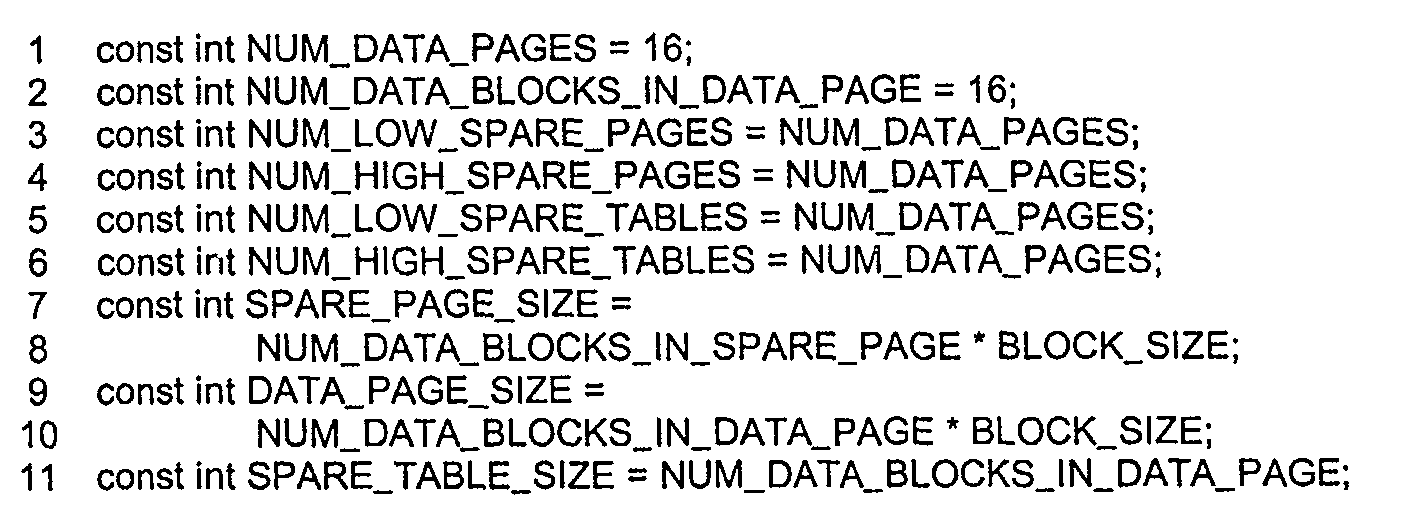
number of data pages = 2page-index field size
number of data blocks in a data page = 2data-block-index field size
The remaining derived constants are straightforwardly derived from the fundamental constants and are literally named, and will therefore not be described further.







Claims (10)
- A solid-state storage device comprising:a physical electronic memory including a spare table region (201-205) containing spare tables (201, 205), a spare page region (202, 204) containing spare pages, and a data page region (203) containing data pages;an electronic memory interface that provides, to devices that access the electronic memory, memory operations directed to target data blocks specified by the accessing device via a logical data block address; anda logic component that maps a logical data block address (302) to a physical address describing the location of a data block in the electronic memory.
- The solid-state storage device of claim 1 wherein a logical data block address (302) comprises:a page index (304) that indexes a data page within the data page region, a spare table within the spare table region, and a spare page within the spare page region; anda data block index (303) that indexes a data block within the data page indexed by the page index and a spare table element within the spare table indexed by the page index.
- The solid-state storage device of claim 2 wherein, in order to map a logical data block address (302) to a physical address, the logic component:extracts the page index (304) and data block index (303) from the logical data block address;uses the page index to locate a corresponding spare table (301);uses the data block index to locate a corresponding spare table element (306) within the corresponding spare table;when a status indication within the corresponding spare table element indicates that the logical data block address has been remapped,
uses a page offset within the corresponding spare table element and the page index extracted from the logical data block address to determine the physical address of a data block (308), within a spare page (307), that corresponds to the logical data block address (302); andwhen a status indication within the corresponding spare table element (306) indicates that the logical data block address has not been remapped,
uses the page index and data block index to determine the physical address of a data block (310), within a data page (309), that corresponds to the logical data block address. - The solid-state storage device of claim 2, further including a spare table cache and a cached spare table identifier register,
wherein the electronic memory includes:wherein the first spare table region (201) occupies a first, lower addressed portion of the electronic memory, the first spare page region (202) occupies a second, next lower addressed portion of the electronic memory, the data page region (203) occupies a third, middle portion of the electronic memory, the second spare page region (204) occupies a fourth, higher addressed portion of the electronic memory, and the second spare table region (205) occupies a fifth, highest addressed portion of the electronic memory; anda first spare table region (201),a first spare page region (202),a data page region (203),a second spare page region (204), anda second spare table region (205);
wherein redundant copies of the spare tables of the first spare table region (201) are stored in the second spare table region (205). - The solid state storage device of claim 4 wherein, in order to map a logical data block address (302) to a physical address, the logic component:extracts the page index (304) and data block index (303) from the logical data block address;uses the page index to locate a corresponding spare table (301);determines, by comparing the page index extracted from logical data block address to the contents of the spare table identifier register, whether the spare table cache contains the contents of the located corresponding spare table;when the spare table cache does not contain the contents of the located corresponding spare table,
copies the located corresponding spare table into the spare table cache;uses the data block index to locate a corresponding spare table element within the spare table cache;when a status indication within the corresponding spare table element indicates that the logical data block address has been remapped,
uses a page offset within the corresponding spare table element (306) and the page index extracted from the logical data block address to determine the physical address of a data block (308), within a spare page (307), that corresponds to the logical data block address; andwhen a status indication within the corresponding spare table element indicates that the logical data block address has not been remapped,
uses the page index and data block index to determine the physical address of a data block (310), within a data page (309), that corresponds to the logical data block address. - The solid-state storage device of claim 1 wherein a spare table (301) contains a number of elements equal to the number of data blocks (310) in a data page (309), wherein the spare table region contains a number of spare tables (201, 205) equal to the number of data pages within the data page region (203), wherein the spare page region contains a number of spare pages (202, 204) equal to the number of data pages within the data page region (203), and wherein a spare page (307) contains a fixed number of data blocks (308), including a first data block that contains a spare block map that contains spare block map elements that store status information for data blocks stored within the spare page.
- A method for transforming a logical data block address (302) into a physical electronic memory address, the method comprising:providing an electronic memory having a spare table region (201, 205) containing spare tables, a spare page region (202, 204) containing spare pages, and a data page region (203) containing data pages;extracting a page index (304) and a data block index (303) from the logical data block address; andusing the extracted page index and data block index to identify the address of a physical data block (310) within the electronic memory corresponding to the logical data block address.
- The method of claim 7 further including:using the extracted page index (303) as an offset to locate a spare table (301) within the spare table region (201);using the extracted data block index (304) as an offset to locate a spare table element (306) within the spare table (301);when a status indication within the spare table element (306) indicates that the logical data block address has been remapped,
using the page index extracted from the logical data block address to determine the physical address of a spare page (307) within the spare page region (202);using a page offset within the spare table element (306) to determine the physical address of a data block (308) within the spare page (307); andwhen a status indication within the corresponding spare table element indicates that the logical data block address has not been remapped,
using the page index (303) from the logical data block address (302) to determine the physical address of a data page (309) within the data page region (203), andusing the data block index as an offset to determine the physical address of a data block (310) within the data page (309). - The method of claim 8 further including:when a status indication within the spare table element (306) indicates that the logical data block address (302) has been remapped,
using the status indication to determine whether the data block is in a low spare page region (202) or a high spare page region (204) and to select the indicated spare page region,
using the page index (304) extracted from the logical data block address (302) to determine the physical address of a spare page (307) within the selected spare page region (202), and
using a page offset within the spare table element (306) to determine the physical address of a data block (308) within the spare page (307); andafter using the extracted page index (304) as an offset to locate a spare table (301) within the spare table region (201), and before using the extracted data block index (303) as an offset to locate a spare table element (306) within the spare table,
checking a register to determine whether a currently cached spare table corresponds to the logical block address (302), and when the currently cached spare table does not correspond to the logical block address, copying the located spare table within the spare table region to a memory cache. - The method of claim 9 further including:when the currently cached spare table (301) does not correspond to the logical block address (302), and when the contents of the currently cached spare table (301) has been changed since the currently cached spare table was copied to the memory cache, copying the currently cached spare table back to the spare table region (202) prior to copying the located spare table within the spare table region to the memory cache.
Applications Claiming Priority (2)
| Application Number | Priority Date | Filing Date | Title |
|---|---|---|---|
| US746328 | 1991-08-16 | ||
| US09/746,328 US7013376B2 (en) | 2000-12-20 | 2000-12-20 | Method and system for data block sparing in a solid-state storage device |
Publications (2)
| Publication Number | Publication Date |
|---|---|
| EP1217524A2 true EP1217524A2 (en) | 2002-06-26 |
| EP1217524A3 EP1217524A3 (en) | 2002-12-04 |
Family
ID=25000356
Family Applications (1)
| Application Number | Title | Priority Date | Filing Date |
|---|---|---|---|
| EP01310297A Withdrawn EP1217524A3 (en) | 2000-12-20 | 2001-12-10 | Method and system for data block sparing in a solid-state storage device |
Country Status (4)
| Country | Link |
|---|---|
| US (1) | US7013376B2 (en) |
| EP (1) | EP1217524A3 (en) |
| JP (1) | JP2002215468A (en) |
| KR (1) | KR20020050163A (en) |
Cited By (8)
| Publication number | Priority date | Publication date | Assignee | Title |
|---|---|---|---|---|
| CN112908402A (en) * | 2021-03-31 | 2021-06-04 | 长鑫存储技术有限公司 | Spare circuit allocation method, device, equipment and medium |
| US11791012B2 (en) | 2021-03-31 | 2023-10-17 | Changxin Memory Technologies, Inc. | Standby circuit dispatch method, apparatus, device and medium |
| US11791010B2 (en) | 2020-08-18 | 2023-10-17 | Changxin Memory Technologies, Inc. | Method and device for fail bit repairing |
| US11797371B2 (en) | 2020-08-18 | 2023-10-24 | Changxin Memory Technologies, Inc. | Method and device for determining fail bit repair scheme |
| US11853152B2 (en) | 2020-08-18 | 2023-12-26 | Changxin Memory Technologies, Inc. | Fail bit repair method and device |
| US11881278B2 (en) | 2021-03-31 | 2024-01-23 | Changxin Memory Technologies, Inc. | Redundant circuit assigning method and device, apparatus and medium |
| US11887685B2 (en) | 2020-08-18 | 2024-01-30 | Changxin Memory Technologies, Inc. | Fail Bit repair method and device |
| US11984179B2 (en) | 2021-03-26 | 2024-05-14 | Changxin Memory Technologies, Inc. | Redundant circuit assigning method and device, and medium |
Families Citing this family (63)
| Publication number | Priority date | Publication date | Assignee | Title |
|---|---|---|---|---|
| TW200523946A (en) * | 2004-01-13 | 2005-07-16 | Ali Corp | Method for accessing a nonvolatile memory |
| US7664983B2 (en) | 2004-08-30 | 2010-02-16 | Symantec Corporation | Systems and methods for event driven recovery management |
| US7363316B2 (en) | 2004-08-30 | 2008-04-22 | Mendocino Software, Inc. | Systems and methods for organizing and mapping data |
| JP2006285600A (en) * | 2005-03-31 | 2006-10-19 | Tokyo Electron Device Ltd | Storage device, memory management device, memory management method, and program |
| TWI298836B (en) * | 2005-10-12 | 2008-07-11 | Sunplus Technology Co Ltd | Apparatus for controlling flash memory and method thereof |
| KR100818797B1 (en) | 2006-10-19 | 2008-04-01 | 삼성전자주식회사 | Memory capacity control method and memory capacity control device |
| US8489817B2 (en) | 2007-12-06 | 2013-07-16 | Fusion-Io, Inc. | Apparatus, system, and method for caching data |
| US9734086B2 (en) | 2006-12-06 | 2017-08-15 | Sandisk Technologies Llc | Apparatus, system, and method for a device shared between multiple independent hosts |
| US8443134B2 (en) | 2006-12-06 | 2013-05-14 | Fusion-Io, Inc. | Apparatus, system, and method for graceful cache device degradation |
| US8935302B2 (en) | 2006-12-06 | 2015-01-13 | Intelligent Intellectual Property Holdings 2 Llc | Apparatus, system, and method for data block usage information synchronization for a non-volatile storage volume |
| US9104599B2 (en) | 2007-12-06 | 2015-08-11 | Intelligent Intellectual Property Holdings 2 Llc | Apparatus, system, and method for destaging cached data |
| US8706968B2 (en) | 2007-12-06 | 2014-04-22 | Fusion-Io, Inc. | Apparatus, system, and method for redundant write caching |
| US7836226B2 (en) | 2007-12-06 | 2010-11-16 | Fusion-Io, Inc. | Apparatus, system, and method for coordinating storage requests in a multi-processor/multi-thread environment |
| US9519540B2 (en) | 2007-12-06 | 2016-12-13 | Sandisk Technologies Llc | Apparatus, system, and method for destaging cached data |
| US8156392B2 (en) | 2008-04-05 | 2012-04-10 | Fusion-Io, Inc. | Apparatus, system, and method for bad block remapping |
| JP5163350B2 (en) | 2008-05-19 | 2013-03-13 | 富士通株式会社 | Verification support program, verification support apparatus, and verification support method |
| US8838876B2 (en) | 2008-10-13 | 2014-09-16 | Micron Technology, Inc. | Translation layer in a solid state storage device |
| US7996736B2 (en) * | 2008-10-26 | 2011-08-09 | Sandisk 3D Llc | Bad page marking strategy for fast readout in memory |
| US8549218B2 (en) * | 2008-11-10 | 2013-10-01 | Inside Secure | Low cost implementation for small content-addressable memories |
| KR101014149B1 (en) * | 2008-11-13 | 2011-02-14 | (주)인디링스 | Controller for solid state disks to control access to memory banks |
| KR101717644B1 (en) | 2009-09-08 | 2017-03-27 | 샌디스크 테크놀로지스 엘엘씨 | Apparatus, system, and method for caching data on a solid-state storage device |
| US9122579B2 (en) | 2010-01-06 | 2015-09-01 | Intelligent Intellectual Property Holdings 2 Llc | Apparatus, system, and method for a storage layer |
| WO2011031903A2 (en) * | 2009-09-09 | 2011-03-17 | Fusion-Io, Inc. | Apparatus, system, and method for allocating storage |
| KR101086876B1 (en) * | 2009-09-30 | 2011-11-25 | 주식회사 하이닉스반도체 | Semiconductor storage system that manages spare area flexibly and its control method |
| US8874981B2 (en) * | 2010-05-12 | 2014-10-28 | Mediatek Inc. | Method of creating target storage layout table referenced for partitioning storage space of storage device and related electronic device and machine-readable medium |
| KR101077901B1 (en) * | 2010-07-12 | 2011-10-31 | (주)이더블유비엠코리아 | Apparatus and method for managing flash memory using log block unit mapping technique |
| US20120239860A1 (en) | 2010-12-17 | 2012-09-20 | Fusion-Io, Inc. | Apparatus, system, and method for persistent data management on a non-volatile storage media |
| US8966184B2 (en) | 2011-01-31 | 2015-02-24 | Intelligent Intellectual Property Holdings 2, LLC. | Apparatus, system, and method for managing eviction of data |
| US8874823B2 (en) | 2011-02-15 | 2014-10-28 | Intellectual Property Holdings 2 Llc | Systems and methods for managing data input/output operations |
| US9201677B2 (en) | 2011-05-23 | 2015-12-01 | Intelligent Intellectual Property Holdings 2 Llc | Managing data input/output operations |
| US9003104B2 (en) | 2011-02-15 | 2015-04-07 | Intelligent Intellectual Property Holdings 2 Llc | Systems and methods for a file-level cache |
| WO2012116369A2 (en) | 2011-02-25 | 2012-08-30 | Fusion-Io, Inc. | Apparatus, system, and method for managing contents of a cache |
| KR101603004B1 (en) * | 2011-03-16 | 2016-03-11 | 휴렛-팩커드 디벨롭먼트 컴퍼니, 엘.피. | Systems and methods for fine granularity memory sparing |
| US9563555B2 (en) | 2011-03-18 | 2017-02-07 | Sandisk Technologies Llc | Systems and methods for storage allocation |
| US8966191B2 (en) | 2011-03-18 | 2015-02-24 | Fusion-Io, Inc. | Logical interface for contextual storage |
| US9069477B1 (en) * | 2011-06-16 | 2015-06-30 | Amazon Technologies, Inc. | Reuse of dynamically allocated memory |
| US9274937B2 (en) | 2011-12-22 | 2016-03-01 | Longitude Enterprise Flash S.A.R.L. | Systems, methods, and interfaces for vector input/output operations |
| US9767032B2 (en) | 2012-01-12 | 2017-09-19 | Sandisk Technologies Llc | Systems and methods for cache endurance |
| US9251052B2 (en) | 2012-01-12 | 2016-02-02 | Intelligent Intellectual Property Holdings 2 Llc | Systems and methods for profiling a non-volatile cache having a logical-to-physical translation layer |
| US10102117B2 (en) | 2012-01-12 | 2018-10-16 | Sandisk Technologies Llc | Systems and methods for cache and storage device coordination |
| US9251086B2 (en) | 2012-01-24 | 2016-02-02 | SanDisk Technologies, Inc. | Apparatus, system, and method for managing a cache |
| US9116812B2 (en) | 2012-01-27 | 2015-08-25 | Intelligent Intellectual Property Holdings 2 Llc | Systems and methods for a de-duplication cache |
| US10019353B2 (en) * | 2012-03-02 | 2018-07-10 | Longitude Enterprise Flash S.A.R.L. | Systems and methods for referencing data on a storage medium |
| US10339056B2 (en) | 2012-07-03 | 2019-07-02 | Sandisk Technologies Llc | Systems, methods and apparatus for cache transfers |
| US9612966B2 (en) | 2012-07-03 | 2017-04-04 | Sandisk Technologies Llc | Systems, methods and apparatus for a virtual machine cache |
| US10346095B2 (en) | 2012-08-31 | 2019-07-09 | Sandisk Technologies, Llc | Systems, methods, and interfaces for adaptive cache persistence |
| US10318495B2 (en) | 2012-09-24 | 2019-06-11 | Sandisk Technologies Llc | Snapshots for a non-volatile device |
| US10509776B2 (en) | 2012-09-24 | 2019-12-17 | Sandisk Technologies Llc | Time sequence data management |
| US9141613B2 (en) * | 2012-10-30 | 2015-09-22 | Appsense Limited | Systems and methods for determining an address for a private function |
| US9842053B2 (en) | 2013-03-15 | 2017-12-12 | Sandisk Technologies Llc | Systems and methods for persistent cache logging |
| US10558561B2 (en) | 2013-04-16 | 2020-02-11 | Sandisk Technologies Llc | Systems and methods for storage metadata management |
| US10102144B2 (en) | 2013-04-16 | 2018-10-16 | Sandisk Technologies Llc | Systems, methods and interfaces for data virtualization |
| US9842128B2 (en) | 2013-08-01 | 2017-12-12 | Sandisk Technologies Llc | Systems and methods for atomic storage operations |
| US10019320B2 (en) | 2013-10-18 | 2018-07-10 | Sandisk Technologies Llc | Systems and methods for distributed atomic storage operations |
| US10073630B2 (en) | 2013-11-08 | 2018-09-11 | Sandisk Technologies Llc | Systems and methods for log coordination |
| US9946607B2 (en) | 2015-03-04 | 2018-04-17 | Sandisk Technologies Llc | Systems and methods for storage error management |
| KR20190069806A (en) * | 2017-12-12 | 2019-06-20 | 에스케이하이닉스 주식회사 | Memory system and operating method of memory system |
| US11138105B2 (en) * | 2018-12-18 | 2021-10-05 | Seagate Technology Llc | Large range defect allocation system and method |
| WO2020240225A1 (en) * | 2019-05-31 | 2020-12-03 | Micron Technology, Inc. | Embedded flash memory architecture implementing interconnection redundancy |
| CN111190817B (en) * | 2019-12-23 | 2022-09-06 | 深圳平安医疗健康科技服务有限公司 | Method and device for processing software defects |
| CN114138201B (en) * | 2021-12-02 | 2024-10-25 | 国网山东省电力公司营销服务中心(计量中心) | Electric energy meter built-in memory data storage monitoring method and system |
| KR102706442B1 (en) * | 2021-12-23 | 2024-09-11 | 재단법인대구경북과학기술원 | Ssd device and operating method of the same using ftl based on lsm-tree and approximate indexing |
| US12007842B2 (en) * | 2022-10-06 | 2024-06-11 | Salesforce, Inc. | Database node soft restart |
Family Cites Families (7)
| Publication number | Priority date | Publication date | Assignee | Title |
|---|---|---|---|---|
| DE69024086T2 (en) | 1989-04-13 | 1996-06-20 | Sundisk Corp | EEprom system with block deletion |
| US5907856A (en) | 1995-07-31 | 1999-05-25 | Lexar Media, Inc. | Moving sectors within a block of information in a flash memory mass storage architecture |
| US5933852A (en) * | 1996-11-07 | 1999-08-03 | Micron Electronics, Inc. | System and method for accelerated remapping of defective memory locations |
| US6000006A (en) * | 1997-08-25 | 1999-12-07 | Bit Microsystems, Inc. | Unified re-map and cache-index table with dual write-counters for wear-leveling of non-volatile flash RAM mass storage |
| US6269432B1 (en) * | 1998-10-23 | 2001-07-31 | Ericsson, Inc. | Distributed transactional processing system having redundant data |
| US6535995B1 (en) * | 1999-03-10 | 2003-03-18 | International Business Machines Corporation | Prototype-based virtual in-line sparing |
| US6397292B1 (en) * | 1999-08-19 | 2002-05-28 | Emc Corporation | Asymmetrical striping of mirrored storage device arrays and concurrent access to even tracks in the first array and odd tracks in the second array to improve data access performance |
-
2000
- 2000-12-20 US US09/746,328 patent/US7013376B2/en not_active Expired - Lifetime
-
2001
- 2001-11-02 JP JP2001337595A patent/JP2002215468A/en not_active Withdrawn
- 2001-12-10 EP EP01310297A patent/EP1217524A3/en not_active Withdrawn
- 2001-12-19 KR KR1020010081273A patent/KR20020050163A/en not_active Withdrawn
Cited By (9)
| Publication number | Priority date | Publication date | Assignee | Title |
|---|---|---|---|---|
| US11791010B2 (en) | 2020-08-18 | 2023-10-17 | Changxin Memory Technologies, Inc. | Method and device for fail bit repairing |
| US11797371B2 (en) | 2020-08-18 | 2023-10-24 | Changxin Memory Technologies, Inc. | Method and device for determining fail bit repair scheme |
| US11853152B2 (en) | 2020-08-18 | 2023-12-26 | Changxin Memory Technologies, Inc. | Fail bit repair method and device |
| US11887685B2 (en) | 2020-08-18 | 2024-01-30 | Changxin Memory Technologies, Inc. | Fail Bit repair method and device |
| US11984179B2 (en) | 2021-03-26 | 2024-05-14 | Changxin Memory Technologies, Inc. | Redundant circuit assigning method and device, and medium |
| CN112908402A (en) * | 2021-03-31 | 2021-06-04 | 长鑫存储技术有限公司 | Spare circuit allocation method, device, equipment and medium |
| CN112908402B (en) * | 2021-03-31 | 2022-05-10 | 长鑫存储技术有限公司 | Backup circuit assignment method, apparatus, apparatus and medium |
| US11791012B2 (en) | 2021-03-31 | 2023-10-17 | Changxin Memory Technologies, Inc. | Standby circuit dispatch method, apparatus, device and medium |
| US11881278B2 (en) | 2021-03-31 | 2024-01-23 | Changxin Memory Technologies, Inc. | Redundant circuit assigning method and device, apparatus and medium |
Also Published As
| Publication number | Publication date |
|---|---|
| KR20020050163A (en) | 2002-06-26 |
| JP2002215468A (en) | 2002-08-02 |
| US7013376B2 (en) | 2006-03-14 |
| EP1217524A3 (en) | 2002-12-04 |
| US20020120824A1 (en) | 2002-08-29 |
Similar Documents
| Publication | Publication Date | Title |
|---|---|---|
| US7013376B2 (en) | Method and system for data block sparing in a solid-state storage device | |
| EP1183606B1 (en) | Address mapping in solid state storage device | |
| US5956473A (en) | Method and system for managing a flash memory mass storage system | |
| US5974564A (en) | Method for remapping defective memory bit sets to non-defective memory bit sets | |
| US6285607B1 (en) | Memory system | |
| US6694415B2 (en) | Methods for permanently preventing modification of a partition or file | |
| US7546515B2 (en) | Method of storing downloadable firmware on bulk media | |
| US9916116B2 (en) | Memory access and detecting memory failures using dynamically replicated memory based on a replication policy | |
| US7536627B2 (en) | Storing downloadable firmware on bulk media | |
| US5684986A (en) | Embedded directory method and record for direct access storage device (DASD) data compression | |
| US20050015557A1 (en) | Nonvolatile memory unit with specific cache | |
| US20090313453A1 (en) | Data conflict resolution for solid-state memory devices | |
| US6237110B1 (en) | Apparatus and method accessing flash memory | |
| US7590899B2 (en) | Processor memory array having memory macros for relocatable store protect keys | |
| KR100757128B1 (en) | Memory card using flash memory and controlling method thereof | |
| US7634708B2 (en) | Relocatable storage protect keys for system main memory | |
| CN117407325B (en) | Data management method and system supporting SSD | |
| HK1008584B (en) | Error management processes for flash eeprom memory arrays |
Legal Events
| Date | Code | Title | Description |
|---|---|---|---|
| PUAI | Public reference made under article 153(3) epc to a published international application that has entered the european phase |
Free format text: ORIGINAL CODE: 0009012 |
|
| AK | Designated contracting states |
Kind code of ref document: A2 Designated state(s): AT BE CH CY DE DK ES FI FR GB GR IE IT LI LU MC NL PT SE TR |
|
| AX | Request for extension of the european patent |
Free format text: AL;LT;LV;MK;RO;SI |
|
| RIC1 | Information provided on ipc code assigned before grant |
Free format text: 7G 06F 12/02 A, 7G 06F 3/06 B, 7G 06F 12/10 B |
|
| PUAL | Search report despatched |
Free format text: ORIGINAL CODE: 0009013 |
|
| AK | Designated contracting states |
Kind code of ref document: A3 Designated state(s): AT BE CH CY DE DK ES FI FR GB GR IE IT LI LU MC NL PT SE TR |
|
| AX | Request for extension of the european patent |
Free format text: AL;LT;LV;MK;RO;SI |
|
| 17P | Request for examination filed |
Effective date: 20030220 |
|
| AKX | Designation fees paid |
Designated state(s): DE FR GB |
|
| 17Q | First examination report despatched |
Effective date: 20041129 |
|
| STAA | Information on the status of an ep patent application or granted ep patent |
Free format text: STATUS: THE APPLICATION HAS BEEN WITHDRAWN |
|
| 18W | Application withdrawn |
Effective date: 20050930 |