EP1217513A2 - Method for handling 32 bit results for an out-of-order processor with a 64 bit architecture - Google Patents
Method for handling 32 bit results for an out-of-order processor with a 64 bit architecture Download PDFInfo
- Publication number
- EP1217513A2 EP1217513A2 EP01128990A EP01128990A EP1217513A2 EP 1217513 A2 EP1217513 A2 EP 1217513A2 EP 01128990 A EP01128990 A EP 01128990A EP 01128990 A EP01128990 A EP 01128990A EP 1217513 A2 EP1217513 A2 EP 1217513A2
- Authority
- EP
- European Patent Office
- Prior art keywords
- instruction
- bit
- result
- extract
- bitlength
- Prior art date
- Legal status (The legal status is an assumption and is not a legal conclusion. Google has not performed a legal analysis and makes no representation as to the accuracy of the status listed.)
- Withdrawn
Links
Images




Classifications
-
- G—PHYSICS
- G06—COMPUTING OR CALCULATING; COUNTING
- G06F—ELECTRIC DIGITAL DATA PROCESSING
- G06F9/00—Arrangements for program control, e.g. control units
- G06F9/06—Arrangements for program control, e.g. control units using stored programs, i.e. using an internal store of processing equipment to receive or retain programs
- G06F9/30—Arrangements for executing machine instructions, e.g. instruction decode
- G06F9/3017—Runtime instruction translation, e.g. macros
-
- G—PHYSICS
- G06—COMPUTING OR CALCULATING; COUNTING
- G06F—ELECTRIC DIGITAL DATA PROCESSING
- G06F9/00—Arrangements for program control, e.g. control units
- G06F9/06—Arrangements for program control, e.g. control units using stored programs, i.e. using an internal store of processing equipment to receive or retain programs
- G06F9/30—Arrangements for executing machine instructions, e.g. instruction decode
- G06F9/30003—Arrangements for executing specific machine instructions
- G06F9/30007—Arrangements for executing specific machine instructions to perform operations on data operands
- G06F9/30032—Movement instructions, e.g. MOVE, SHIFT, ROTATE, SHUFFLE
-
- G—PHYSICS
- G06—COMPUTING OR CALCULATING; COUNTING
- G06F—ELECTRIC DIGITAL DATA PROCESSING
- G06F9/00—Arrangements for program control, e.g. control units
- G06F9/06—Arrangements for program control, e.g. control units using stored programs, i.e. using an internal store of processing equipment to receive or retain programs
- G06F9/30—Arrangements for executing machine instructions, e.g. instruction decode
- G06F9/30003—Arrangements for executing specific machine instructions
- G06F9/30007—Arrangements for executing specific machine instructions to perform operations on data operands
- G06F9/30036—Instructions to perform operations on packed data, e.g. vector, tile or matrix operations
-
- G—PHYSICS
- G06—COMPUTING OR CALCULATING; COUNTING
- G06F—ELECTRIC DIGITAL DATA PROCESSING
- G06F9/00—Arrangements for program control, e.g. control units
- G06F9/06—Arrangements for program control, e.g. control units using stored programs, i.e. using an internal store of processing equipment to receive or retain programs
- G06F9/30—Arrangements for executing machine instructions, e.g. instruction decode
- G06F9/30098—Register arrangements
- G06F9/30105—Register structure
- G06F9/30112—Register structure comprising data of variable length
-
- G—PHYSICS
- G06—COMPUTING OR CALCULATING; COUNTING
- G06F—ELECTRIC DIGITAL DATA PROCESSING
- G06F9/00—Arrangements for program control, e.g. control units
- G06F9/06—Arrangements for program control, e.g. control units using stored programs, i.e. using an internal store of processing equipment to receive or retain programs
- G06F9/30—Arrangements for executing machine instructions, e.g. instruction decode
- G06F9/38—Concurrent instruction execution, e.g. pipeline or look ahead
- G06F9/3824—Operand accessing
-
- G—PHYSICS
- G06—COMPUTING OR CALCULATING; COUNTING
- G06F—ELECTRIC DIGITAL DATA PROCESSING
- G06F9/00—Arrangements for program control, e.g. control units
- G06F9/06—Arrangements for program control, e.g. control units using stored programs, i.e. using an internal store of processing equipment to receive or retain programs
- G06F9/30—Arrangements for executing machine instructions, e.g. instruction decode
- G06F9/38—Concurrent instruction execution, e.g. pipeline or look ahead
- G06F9/3836—Instruction issuing, e.g. dynamic instruction scheduling or out of order instruction execution
-
- G—PHYSICS
- G06—COMPUTING OR CALCULATING; COUNTING
- G06F—ELECTRIC DIGITAL DATA PROCESSING
- G06F9/00—Arrangements for program control, e.g. control units
- G06F9/06—Arrangements for program control, e.g. control units using stored programs, i.e. using an internal store of processing equipment to receive or retain programs
- G06F9/30—Arrangements for executing machine instructions, e.g. instruction decode
- G06F9/38—Concurrent instruction execution, e.g. pipeline or look ahead
- G06F9/3836—Instruction issuing, e.g. dynamic instruction scheduling or out of order instruction execution
- G06F9/3838—Dependency mechanisms, e.g. register scoreboarding
-
- G—PHYSICS
- G06—COMPUTING OR CALCULATING; COUNTING
- G06F—ELECTRIC DIGITAL DATA PROCESSING
- G06F9/00—Arrangements for program control, e.g. control units
- G06F9/06—Arrangements for program control, e.g. control units using stored programs, i.e. using an internal store of processing equipment to receive or retain programs
- G06F9/30—Arrangements for executing machine instructions, e.g. instruction decode
- G06F9/38—Concurrent instruction execution, e.g. pipeline or look ahead
- G06F9/3836—Instruction issuing, e.g. dynamic instruction scheduling or out of order instruction execution
- G06F9/3838—Dependency mechanisms, e.g. register scoreboarding
- G06F9/384—Register renaming
-
- G—PHYSICS
- G06—COMPUTING OR CALCULATING; COUNTING
- G06F—ELECTRIC DIGITAL DATA PROCESSING
- G06F9/00—Arrangements for program control, e.g. control units
- G06F9/06—Arrangements for program control, e.g. control units using stored programs, i.e. using an internal store of processing equipment to receive or retain programs
- G06F9/30—Arrangements for executing machine instructions, e.g. instruction decode
- G06F9/38—Concurrent instruction execution, e.g. pipeline or look ahead
- G06F9/3854—Instruction completion, e.g. retiring, committing or graduating
-
- G—PHYSICS
- G06—COMPUTING OR CALCULATING; COUNTING
- G06F—ELECTRIC DIGITAL DATA PROCESSING
- G06F9/00—Arrangements for program control, e.g. control units
- G06F9/06—Arrangements for program control, e.g. control units using stored programs, i.e. using an internal store of processing equipment to receive or retain programs
- G06F9/30—Arrangements for executing machine instructions, e.g. instruction decode
- G06F9/38—Concurrent instruction execution, e.g. pipeline or look ahead
- G06F9/3854—Instruction completion, e.g. retiring, committing or graduating
- G06F9/3856—Reordering of instructions, e.g. using queues or age tags
-
- G—PHYSICS
- G06—COMPUTING OR CALCULATING; COUNTING
- G06F—ELECTRIC DIGITAL DATA PROCESSING
- G06F9/00—Arrangements for program control, e.g. control units
- G06F9/06—Arrangements for program control, e.g. control units using stored programs, i.e. using an internal store of processing equipment to receive or retain programs
- G06F9/30—Arrangements for executing machine instructions, e.g. instruction decode
- G06F9/38—Concurrent instruction execution, e.g. pipeline or look ahead
- G06F9/3854—Instruction completion, e.g. retiring, committing or graduating
- G06F9/3858—Result writeback, i.e. updating the architectural state or memory
Definitions
- the present invention relates to an improvement of out-of-order CPU architecture regarding code flexibility.
- it relates to a method for operating an out-of-order processor having an architecture of a larger bitlength with a program comprising instructions compiled to produce instruction results of a smaller bitlength.
- the present invention has a quite general scope which is not limited to a vendor-specific processor architecture because its key concepts are independent therefrom.
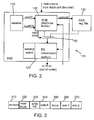
- FIG.1 a schematically depicted prior art out-of-order processor 100 - in this example a IBM S/390 processor - has as an essential component a so-called Instruction Window Buffer, further referred to herein as IWB, too. This is depicted in fig. 1 with reference sign 110.
- IWB Instruction Window Buffer
- the instructions after the instructions have been fetched by a fetch unit 170, stored in the instruction queue 140 and have been renamed in a renaming unit 115, see Fig. 2, they are stored in-order into a part of the IWB called reservation station 120. From the reservation station the instructions may be issued out-of-order to a plurality of instruction execution units 180 abbreviated herein as IEU, and the speculative results are stored in a temporary register buffer, called reorder buffer 125, abbreviated herein as (ROB). These speculative results are committed (or retired) in the actual program order thereby transforming the speculative result into the architectural state within a register file 130, a so-called Architected Register Array (ARA). In this way it is assured that the out-of-order processor with respect to its architectural state behaves like an in-order processor.
- the communication between rename unit reservation station, reorder buffer and register file is done with a multiplexor element 150.
- the IWB pipeline is depicted in fig. 3 and starts with renaming, 310, said up to 4 dispatched instructions.
- the renaming process translates the source logical register address into a physical address specifying where the speculative result resides or will be stored after execution. Furthermore, it allocates new ROB entries for the storage of the speculative results after execution of the dispatched instructions.
- the detection of a dependency of a source register with the target register of an instruction that resides in the IWB is done by the renaming logic by comparing the source operand register addresses with the target operand register addresses stored for each entry.
- match[0..63] signals generated for each entry are ANDed with a so called "current_bit[0..63]".
- a current_bit[i] is only ON when an instruction i is the youngest instruction in the IWB for the specific logical target register address. It should be noted that ANDing the match[0..63] with the current_bit[0..63] string - thereby generating the RSEL[0..63] string in fig. 2 - is needed, since several matches may be found for the same logical target address. However, only the match with the youngest instructions specifies the correct dependency.
- a priority filter logic could be used to filter out the youngest match and thereby generating the RSEL[0..63] for an operand.
- the generation of the RSEL[0..63] string has been described here for a single operand, but it will be clear that in case when more operands or more instructions are renamed, then for each operand such a RSEL[0..63] string is generated.
- the RSEL[0..63] selects the Reorder Buffer (ROB).
- ROB Reorder Buffer
- the tag, data validity bit and target data will appear at the output ports of the ROB 125 for each source operand at the end of the second cycle.
- the tag, validity and data may not be read in the same cycle. In other words, after the read out of the tag, the read out of the data or the validity bits may be realized in separate cycles to maintain the consistency of the data between reorder buffer ROB 125 and reservation station 120.
- the tag, validity and data is written into the reservation 220 -entry allocated to the renamed instructions.
- the write of data in the reservation station may be delayed for the validity and data bits dependent on the protocol for tag and data of the IEU's.
- the "select" cycle 340 the instructions for which the data was written into the reservation station in the previous cycle will be included into the set of instructions that are considered by the select logic for issue.
- the select logic selects the oldest instruction that waits for issue for each IEU. This logic is implemented by a priority filter like it is described in the above referenced patent application.
- a string issue[0..63] is generated for the IEUs.
- the generation of one or more issue[0..63] strings by the select logic ends the select cycle. It should be noted that the select logic may select the instruction for issue out of the normal program order for execution dependent on the availability of the source data for each instruction.
- issue[0..63] strings specify the RS entry that has to be read out, and at the end of the cycle the data, control, tag, etc. bits will appear at the RS ports to the IEUs.
- the execution of the instruction is done in the cycles "exe 1" ,360 and "exe 2" 370.
- the tags, specifying the entry where the data has to be stored in the ROB 125 and the RS 120, are compared with the stored tags for the sources. In case of a match the validity bit is set and the result data is stored in the sources of the dependent instruction in the RS.
- the commit process will free-up the IWB entries in the original program order by copying the data from the ROB to the ARA 130. As soon as the data has been written into the ARA it has become the architectural state of the processor and the IWB entries can be used again to store the new instructions dispatched by the fetch unit.
- the prior art processor cited above has a 32-bit architecture. It is, however desirable that a 64 bit architecture still supports former 32 bit instructions originating from the use of earlier developed programs. Thus, predetermined protocol convention exist in prior art that in case of writing a 32-bit result into a 64-bit register the 'overhanging' bits have to remain unchanged. For most of the instructions this creates no particular problem, since for most instructions one of the source registers 410, 415 is the same as the target register 420. Hence, the unchanged 32-bit of the result 0..31 is available as input to the execution unit and it can be used to set the 32 bit part of the 64 bit result that does not have to be calculated. A problem now occurs in a 64-bit architecture for those instructions that do not have the result register as their respective input.
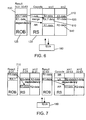
- Load Address For the exemplary Load Address instruction "LA R1, D2(X2,B2)" the address specified by the X2, B2 and D2 fields is placed in the general register R1. Thereby, the address is a 32-bit result and the bits 0-31 of R1 have to remain unchanged. In an in-order processor, the implementation of the leaving bits 0-31 to be unchanged could be accomplished by only writing bits 32-63 in the register R1. In an out-of-order processor, however, the IWB can contain many instructions at a time with their speculative results being calculated. Since the LA instruction may be followed by a 64 bit instruction that has as a source R1 dependent on the LA instruction result, all 64 bit need to be available in the Reservation station.
- the problem is solved by first writing the 32-bit result of the LA execution into the temporary register 610, here called RX.
- the merge instruction 620 has this register as its source input together with the R1-data in which the result of the LA register has to be written.
- the merge instruction will be issued next and the IEU will merge the bits 0-31 of the R1-data, i.e., the unchanged bits and the bits 32-63 of the RX-data into the 64 bit result for the R1 register. Since the AR instruction 540 still has a dependency on the R1 register it now will receive the required full 64-bit result of the merge instruction as its source operand.
- the present invention discloses a method and a respective exemplary implementation scheme to handle instructions in an out-of-order processor that write a 32-bit result into a 64-bit wide register.
- the 64-bit architecture specifies that the 64-bit result has to be constructed from the 32-bit result by leaving the remaining, i.e., overhanging 32 bits unchanged.
- extract instruction is disclosed which writes the 'overhanging' bit portion not into its own result field but in the result field of the subsequent -here a LA- instruction.
- an inventional method for operating a processor having an architecture of a larger bitlength with a program comprising instructions compiled to produce instruction results of a smaller bitlength which comprises the following essential steps:
- the main advantage is that the extract instruction can be executed independently of the following LA - or other - instruction whereby the above mentioned problems are solved nearly without performance loss or increase of chip area of a respective implementation of reservation station and reorder buffer.
- the step of writing the extract instruction result into the result field of said first instruction is controlled by incrementing a tag specifying in which location the result of the first instruction has to be written.
- the inventional method can be applied to cases in which the larger bitlength is 64-bit and the smaller bitlength is 32-bit, or in which the larger bitlength is 128-bit and the smaller bitlength is 64 or 32-bit, even when code combinations of more than one smaller bitlength is present.
- the inventional method can be varied and/ or improved by selectively inserting an extract instruction according to the above concept, only when said second instruction is dependent of the first instruction. This means, in particular, checking if the second instruction uses the target register of the first instruction as a source register, and if it is used then inserting said extract instruction into the instruction scheme. This can be advantageously applied when these occurrences can be appreciated to be quite rare, in advance.
- the method according to its primary aspect can be extended to further comprising the steps ofdispatching said LA instruction in the same cycle as the extract instruction. Then, in the same cycle both of said two instructions write the results into the RS, causing a multiple write into the same result register.
- the above procedure can be performed either whenever a 32 bit result is written into a 64-bit register, -or this can be selectively performed only when said result register is used for a subsequent 64-bit instruction as a source register, i.e., in case of the above mentioned write after read or write after write dependency problems.
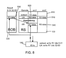
- FIG. 8 With general reference to the figures and with special reference now to Fig. 8 the structural elements of the inventional processor design according to a preferred embodiment thereof is described in more detail. The general aspect of this schema is independent of a particular processor chip realization.
- the extract instruction 810 has the result register 530 of the LA instruction as its source operand 820. This enables the IEU 180 to route the R1 data bit 0-31 to its output.
- the other bits 32-63 will be set to '00...00' assuming ORing (or alternatively "11... 11", if ANDing) within the cell, by the IEU during the execution of the extract instruction.
- the IEU 180 sets a control bit indicating that only the 'overhanging' bits 0-31 of the result needs to be written into the ROB 225 and into the other dependent operands of the RS 220. Finally, the IEU increments the tag in a wrap-around fashion specifying into which location of the ROB the result has to be written.
- the extract instruction writes the result into the result field of the LA instruction 510 as well as in all reservation station fields of dependent operands.
- the RS fields of dependent operands are written by comparing tags. Therefore, the result is correctly written into the ROB 225 and the RS 120 when the tag is incremented. Instead of doing the increment of the tag by the IEU, as an alternative it can already be incremented by the decoder in the Fetch Unit.
- the advantage of using the extract instruction instead of for example the merge solution shown in Figure 6 is that the extract can be executed independent of the LA instruction. Since, the extract instruction writes the bits that have to remain unchanged, these bits are usually available even before the LA instruction starts execution. Simulations modeling the performance degradation of this solution ( ⁇ 1%), showed a very minor performance impact for this solution.
- Figure 9 shows the latches 910, 920 of a 64-bit data field together with the logic - left part of the figure - that controls the write into the latches.
- a tag 930 is stored for each source operand for which a dependency was found by the renaming logic. This tag is compared each cycle with the ieu0_tag via line 935 and ieu1_tag via line 940. A match tag in the respective comparators 945 and 950 means that the IEU result has to be written into the latches 910, and 920, respectively.
- This IEU0 write is activated by setting the compare result signal ieu0_wsel to ON.
- the IEU1 result write is activated by setting ieu1_wsel to ON.
- control signals ieu[0..1]_wr0_31 and ieu[0..1]_wr_32_63 being input into a decode logic 960 specify if the result has to be written into latches[0..31] and/or latches[32..63] via the control signals wr_enable0_31, denoted as 965, and wr_enable32_63, denoted as 970, respectively.
- ieu0_wr0_31 and ieu0_wr32_63 will be both ON.
- the decode logic sets the signals write_enable0_31 and write_enable32_63 both to ON. This activates the write of data for all 64 bits.
- ieu0_wsel being ON, the data on the bus 975 ieu0_data[0..63] will be written into the latches[0..63].
- ieu0_wr0_31 will be set ON by IEU0 and ieu0_wr32_63 will be OFF.
- the write_enable0_31 is set ON and write_enable32_64 is set OFF. Since the write for bit 32-63 is not enabled, only the data on bus ieu0_data[0..31] will be written into the latches[0..31] when ieu0_wsel is ON. The content of latches[32..63] remains unchanged.
- ieu0_tag equals ieu1_tag and ieu0_wsel and ieu1_wsel will be set ON since both tags match with the tag stored for the data field.
- wr_enable0_31 and wr_enable32_63 will be set ON by the decode logic 960 since the write has to be enabled for latch[0..31] as well as for latch[32..63]. As a result, it is tried to write the ieu0_data and ieu1_data into the same latches[0..63].
- Another solution would be to double the ieu.._wsel lines into a separate ieu.._wsel0_31 and into a ieu.._wsek32..63.
- IEU0 and IEU1 this solution is acceptable since due to the doubling of the wsel signal the two wr_enable_.. Signals are no longer needed.
- the doubling of the wsel signals from for example 8 to 16 (-2 enable) is no longer acceptable and a large amount of extra area is required.
- the present invention solves this problem for the IWB implementation as follows:
- the IEU when generating a 32 bit result, will set the other unrelevant bits to all '000...00'. Furthermore, the latch behavior is modified such that it supports a defined state in the case of multiple writes. This multiple write feature is described next and is illustrated in Figure 10.
- next decision is directed to determine if a 32-bit instruction, not setting the remaining 32 bit of the 64-bit register field to the unchanged value.
- step 1120 In the NO-branch of decision 1120 no such 32 bit instruction is detected. Then it is branched back to step 1120 in order to perform the analysis for the next instruction in the stream.
- the inventional EXTRACT instruction is added into the instruction stream before the 32-bit instruction, step 1130.
- step 1140 the EXTRACT instruction and the 32-bit instruction are both dispatched concurrently .
- step 1155 In its NO-branch the process control waits , step 1155 and monitors the valid bits indicating said availability.
- step 1165 In the YES branch thereof it is checked if an instruction execution unit 180 is free, i.e. is available what yields in turn a decision 1160. In the NO-branch it is waited until an IEU is free, step 1165
- the EXTRACT instruction is issued to a free IEU, step 1170 and it is executed by that in a step 1180.
- step 1190 the before-described tag incrementation takes place in order to locate the register the result is written back to, step 1190.
- the EXTRACT result is written back to the result register of the 64-bit instruction and into all dependent source registers.
- the EXTRACT instruction work is done the whole 64-bit range can now be used for the instruction(s) to follow - for both, a 64-bit as well as for a 32-bit instruction possibly more downstream the instruction stream.
- control flow scheme depicted in fig. 11 can be modified in order to reflect a 'selective adding ' of the extract instruction only when really required - after detection of a combined bit length code, and after detection of the dependency situation described above with reference to fig. 11.
- the same figure is referenced again.
- the next decision is directed to determine if a 32-bit instruction not setting the not calculated 32 bit to the unchanged value -in other words the target address register is not one of the source register address for the instruction - is followed by a 64-bit instruction which is dependent of the 32-bit one.
- step 1120 In the NO-branch of the thus modified question and decision 1120 no dependency is detected. Then it is branched back to step 1120 in order to perform the dependency analysis for the next instruction in the stream.
- the instruction stream is re-fetched starting at the 32 bit instruction, and the inventional EXTRACT instruction is added into the instruction stream before the 32-bit instruction, step 1130.
- the advantage of this method is that the extract instruction is only added when the problem occurs.
- the disadvantage is that instructions are removed from the queue and re-fetched again. So, this method is advantageous when an extract instruction has to be added rather seldom.
- the unrelevant bits could have been set to all '11...11' by modifying the behavior of the latch with AND gates instead of OR gates as depicted above in case of multiple write.
- the present invention disclosed in here applies a LA instruction as an example, only.
- each other instruction returning a 32 bit result into a 64 bit data field for which the bits not written have to remain unchanged can be implemented according to the present invention.
- the number of IEUs was in the example limited to two in order to improve clarity. But also a larger number of IEUs may be connected to the RS.
- the invention was described for the IWB that includes the storage of data into the reservation station queue.
- the result and source data is stored in a separate register File and the source data is read from this file after RS issue.
- the solution presented here is also applicable for such a type of pipeline.
- the execution of the extract instruction will then result in writing the unchanged bits into the location of the register file assigned to the LA instruction instead of into the RS and ROB.
- the extract instruction is selectively inserted into the instruction stream only when required.
- the IWB signals the IFU to re-dispatch the instruction with an extract instruction in case that it is detected that the source of a 64 bit instruction depends on a LA or other instruction which does not set the "unchanged overhanging bits".
Landscapes
- Engineering & Computer Science (AREA)
- Software Systems (AREA)
- Theoretical Computer Science (AREA)
- Physics & Mathematics (AREA)
- General Engineering & Computer Science (AREA)
- General Physics & Mathematics (AREA)
- Mathematical Physics (AREA)
- Advance Control (AREA)
- Executing Machine-Instructions (AREA)
Abstract
Description
As soon as the data has been written into the ARA it has become the architectural state of the processor and the IWB entries can be used again to store the new instructions dispatched by the fetch unit.
A problem now occurs in a 64-bit architecture for those instructions that do not have the result register as their respective input. These instructions for example include a performance critical instruction like "Load Address". For the exemplary Load Address instruction "LA R1, D2(X2,B2)" the address specified by the X2, B2 and D2 fields is placed in the general register R1. Thereby, the address is a 32-bit result and the bits 0-31 of R1 have to remain unchanged. In an in-order processor, the implementation of the leaving bits 0-31 to be unchanged could be accomplished by only writing bits 32-63 in the register R1.
In an out-of-order processor, however, the IWB can contain many instructions at a time with their speculative results being calculated. Since the LA instruction may be followed by a 64 bit instruction that has as a source R1 dependent on the LA instruction result, all 64 bit need to be available in the Reservation station.
After the LA instruction -which is symbolically depicted with the horizontal RS entry 510 - is issued from the
Further, the inventional method can be varied and/ or improved by selectively inserting an extract instruction according to the above concept, only when said second instruction is dependent of the first instruction. This means, in particular, checking if the second instruction uses the target register of the first instruction as a source register, and if it is used then inserting said extract instruction into the instruction scheme. This can be advantageously applied when these occurrences can be appreciated to be quite rare, in advance.
The method according to its primary aspect can be extended to further comprising the steps ofdispatching said LA instruction in the same cycle as the extract instruction. Then, in the same cycle both of said two instructions write the results into the RS, causing a multiple write into the same result register.
Instead of doing the increment of the tag by the IEU, as an alternative it can already be incremented by the decoder in the Fetch Unit.
This case is basically similar to the previous case, but now the bits 32-63 are written first by the LA instruction, and thereafter bits 0-31 are written by the extract instruction.
As discussed before, this case is the rather unusual for programs running on a processor.
Since more than one IEU are attached to the reservation station it is possible too that both instructions are issued in the same cycle but to different IEUs. Since both instruction take the same number of cycles to execute also the result will be returned in the same cycle. Now the situation occurs that the bits 0-31 and bits 32-63 are both written at the same time by different IEUs. This however has complications for the logic controlling the write of the 64-bit data fields. This will be explained further with the help of Figure 9.
As, however, the ieu0_wsel and ieu1_wsel signals can be both ON, the required latch behavior is as shown in Figure 10b. The
In the NO-branch it is waited until an IEU is free, step 1165
- on which a source of the 64-bit instruction is dependent on are removed from the RS and ROB queues.
Claims (9)
- A method for operating a processor having an architecture of a larger bitlength with a program comprising instructions compiled to produce instruction results of at least one smaller bitlength, characterized by the steps of
detecting (1120) when in program order a first smaller bitlength instruction is to be dispatched which does not have the target register address as one of its sources,
adding (1130) a so-called 'extract' instruction (810) into the instruction stream before the smaller bitlength instruction ((510), the extract instruction comprising the following steps of:a.dispatching (1140) the extract instruction together with the following smaller bitlength instruction from the instruction queue (140) into the Reservation Station (120),b. issuing (1180) the extract instruction to an IEU (180) as soon as all source operand data is available and an IEU is available according to respective issue scheme,c. executing (1190) the extract instruction by an available IEU,d. setting (1190) an indication that the result of said instruction needs to be written into the result field (530) of the instruction (510) following the extract instruction,e. writing (1195) the extract instruction result into the result field (530) of said first instruction (510), and into all fields of operands being dependent of said first instruction. - The method according to claim 1 in which the step of writing the extract instruction result into the result field (530) of said first instruction (510), is controlled by incrementing a tag specifying in which location the result (530) of the first instruction has to be written.
- The method according to claim 1 in which the larger bitlength is 64-bit and the smaller bitlength is 32-bit.
- The method according to claim 1 in which the larger bitlength is 128-bit and the smaller bitlength is 64 or 32-bit.
- The method according to claim 1, further comprising the steps of when said second instruction (540) is dependent of the first instruction (510), selectively inserting an extract instruction (810).
- The method according to claim 1, further comprising the steps of dispatching (1140) said first instruction (510) in the same cycle as the extract instruction (810), andassuring that in the same cycle both or none of said two instructions is written into a reservation station means (120), and in case of a multiple write into the same result latch (10120)reducing the respective multiple input signals for the latch by an OR gate (10130) or an AND gate, respectively.
- The method according to claim 1, further comprising the steps of associating the same instruction execution unit to said first and said second instruction.
- A processing system having means for performing the steps of a method according to one of the preceding claims 1 to 7.
- A computer system having an out-of-order processing system according to the preceding claim.
Priority Applications (1)
| Application Number | Priority Date | Filing Date | Title |
|---|---|---|---|
| EP01128990A EP1217513A3 (en) | 2000-12-23 | 2001-12-06 | Method for handling 32 bit results for an out-of-order processor with a 64 bit architecture |
Applications Claiming Priority (3)
| Application Number | Priority Date | Filing Date | Title |
|---|---|---|---|
| EP00128490 | 2000-12-23 | ||
| EP00128490 | 2000-12-23 | ||
| EP01128990A EP1217513A3 (en) | 2000-12-23 | 2001-12-06 | Method for handling 32 bit results for an out-of-order processor with a 64 bit architecture |
Publications (2)
| Publication Number | Publication Date |
|---|---|
| EP1217513A2 true EP1217513A2 (en) | 2002-06-26 |
| EP1217513A3 EP1217513A3 (en) | 2003-08-13 |
Family
ID=26071688
Family Applications (1)
| Application Number | Title | Priority Date | Filing Date |
|---|---|---|---|
| EP01128990A Withdrawn EP1217513A3 (en) | 2000-12-23 | 2001-12-06 | Method for handling 32 bit results for an out-of-order processor with a 64 bit architecture |
Country Status (1)
| Country | Link |
|---|---|
| EP (1) | EP1217513A3 (en) |
Cited By (2)
| Publication number | Priority date | Publication date | Assignee | Title |
|---|---|---|---|---|
| EP3014422A4 (en) * | 2013-06-28 | 2017-03-01 | Intel Corporation | Mode dependent partial width load to wider register processors, methods, and systems |
| EP3060978B1 (en) * | 2013-10-27 | 2021-08-11 | Advanced Micro Devices, Inc. | Processor and methods for floating point register aliasing |
Family Cites Families (3)
| Publication number | Priority date | Publication date | Assignee | Title |
|---|---|---|---|---|
| US5805916A (en) * | 1996-11-27 | 1998-09-08 | International Business Machines Corporation | Method and apparatus for dynamic allocation of registers for intermediate floating-point results |
| US6094719A (en) * | 1997-06-25 | 2000-07-25 | Sun Microsystems, Inc. | Reducing data dependent conflicts by converting single precision instructions into microinstructions using renamed phantom registers in a processor having double precision registers |
| US6493819B1 (en) * | 1999-11-16 | 2002-12-10 | Advanced Micro Devices, Inc. | Merging narrow register for resolution of data dependencies when updating a portion of a register in a microprocessor |
-
2001
- 2001-12-06 EP EP01128990A patent/EP1217513A3/en not_active Withdrawn
Cited By (4)
| Publication number | Priority date | Publication date | Assignee | Title |
|---|---|---|---|---|
| EP3014422A4 (en) * | 2013-06-28 | 2017-03-01 | Intel Corporation | Mode dependent partial width load to wider register processors, methods, and systems |
| CN109508206A (en) * | 2013-06-28 | 2019-03-22 | 英特尔公司 | Processor, the method and system loaded dependent on the partial width of mode is carried out to wider register |
| CN109508206B (en) * | 2013-06-28 | 2023-08-29 | 英特尔公司 | Processor, method and system for mode dependent partial width loading of wider registers |
| EP3060978B1 (en) * | 2013-10-27 | 2021-08-11 | Advanced Micro Devices, Inc. | Processor and methods for floating point register aliasing |
Also Published As
| Publication number | Publication date |
|---|---|
| EP1217513A3 (en) | 2003-08-13 |
Similar Documents
| Publication | Publication Date | Title |
|---|---|---|
| US7228403B2 (en) | Method for handling 32 bit results for an out-of-order processor with a 64 bit architecture | |
| US6920546B2 (en) | Fusion of processor micro-operations | |
| US5699537A (en) | Processor microarchitecture for efficient dynamic scheduling and execution of chains of dependent instructions | |
| US6185671B1 (en) | Checking data type of operands specified by an instruction using attributes in a tagged array architecture | |
| US7937561B2 (en) | Merge microinstruction for minimizing source dependencies in out-of-order execution microprocessor with variable data size macroarchitecture | |
| US5546597A (en) | Ready selection of data dependent instructions using multi-cycle cams in a processor performing out-of-order instruction execution | |
| US5553256A (en) | Apparatus for pipeline streamlining where resources are immediate or certainly retired | |
| US6553480B1 (en) | System and method for managing the execution of instruction groups having multiple executable instructions | |
| KR100819232B1 (en) | In order multithreading recycle and dispatch mechanism | |
| US7392369B2 (en) | Decomposing architectural operation into speculative and architectural micro-operations for speculative execution of others and for violation check | |
| EP0762270B1 (en) | Microprocessor with load/store operation to/from multiple registers | |
| EP3171264B1 (en) | System and method of speculative parallel execution of cache line unaligned load instructions | |
| EP0947917A2 (en) | Method and apparatus for handling imprecise exceptions | |
| US6463524B1 (en) | Superscalar processor and method for incrementally issuing store instructions | |
| EP4730116A1 (en) | Instruction processing method and device, and storage medium and electronic device | |
| US5727177A (en) | Reorder buffer circuit accommodating special instructions operating on odd-width results | |
| US7844799B2 (en) | Method and system for pipeline reduction | |
| JP3611304B2 (en) | Pipeline processor system and method for generating one-cycle pipeline stalls | |
| US6829699B2 (en) | Rename finish conflict detection and recovery | |
| US5812812A (en) | Method and system of implementing an early data dependency resolution mechanism in a high-performance data processing system utilizing out-of-order instruction issue | |
| US20050223201A1 (en) | Facilitating rapid progress while speculatively executing code in scout mode | |
| US5841998A (en) | System and method of processing instructions for a processor | |
| US6473850B1 (en) | System and method for handling instructions occurring after an ISYNC instruction | |
| US5850563A (en) | Processor and method for out-of-order completion of floating-point operations during load/store multiple operations | |
| US20050102494A1 (en) | Method and apparatus for register stack implementation using micro-operations |
Legal Events
| Date | Code | Title | Description |
|---|---|---|---|
| PUAI | Public reference made under article 153(3) epc to a published international application that has entered the european phase |
Free format text: ORIGINAL CODE: 0009012 |
|
| AK | Designated contracting states |
Kind code of ref document: A2 Designated state(s): AT BE CH CY DE DK ES FI FR GB GR IE IT LI LU MC NL PT SE TR |
|
| AX | Request for extension of the european patent |
Free format text: AL;LT;LV;MK;RO;SI |
|
| PUAL | Search report despatched |
Free format text: ORIGINAL CODE: 0009013 |
|
| AK | Designated contracting states |
Designated state(s): AT BE CH CY DE DK ES FI FR GB GR IE IT LI LU MC NL PT SE TR |
|
| AX | Request for extension of the european patent |
Extension state: AL LT LV MK RO SI |
|
| 17P | Request for examination filed |
Effective date: 20031127 |
|
| AKX | Designation fees paid |
Designated state(s): AT BE CH CY DE DK ES FI FR GB GR IE IT LI LU MC NL PT SE TR |
|
| 17Q | First examination report despatched |
Effective date: 20070530 |
|
| RAP1 | Party data changed (applicant data changed or rights of an application transferred) |
Owner name: INTEL CORPORATION |
|
| STAA | Information on the status of an ep patent application or granted ep patent |
Free format text: STATUS: THE APPLICATION IS DEEMED TO BE WITHDRAWN |
|
| 18D | Application deemed to be withdrawn |
Effective date: 20160831 |