EP1215891A1 - Circuit de lecture de charges a préamplification adaptive et procédé de lecture des charges a préamplification adaptive - Google Patents
Circuit de lecture de charges a préamplification adaptive et procédé de lecture des charges a préamplification adaptive Download PDFInfo
- Publication number
- EP1215891A1 EP1215891A1 EP01403217A EP01403217A EP1215891A1 EP 1215891 A1 EP1215891 A1 EP 1215891A1 EP 01403217 A EP01403217 A EP 01403217A EP 01403217 A EP01403217 A EP 01403217A EP 1215891 A1 EP1215891 A1 EP 1215891A1
- Authority
- EP
- European Patent Office
- Prior art keywords
- capacitive means
- voltage
- reading
- capacitive
- terminals
- Prior art date
- Legal status (The legal status is an assumption and is not a legal conclusion. Google has not performed a legal analysis and makes no representation as to the accuracy of the status listed.)
- Withdrawn
Links
- 238000000034 method Methods 0.000 title claims description 7
- 230000005855 radiation Effects 0.000 claims abstract description 8
- 239000003990 capacitor Substances 0.000 claims description 7
- 238000001514 detection method Methods 0.000 abstract description 2
- 238000003384 imaging method Methods 0.000 abstract 1
- 230000010354 integration Effects 0.000 description 13
- 238000010586 diagram Methods 0.000 description 3
- 230000008878 coupling Effects 0.000 description 2
- 238000010168 coupling process Methods 0.000 description 2
- 238000005859 coupling reaction Methods 0.000 description 2
- 238000005516 engineering process Methods 0.000 description 2
- 238000005259 measurement Methods 0.000 description 2
- 230000004313 glare Effects 0.000 description 1
- 238000002347 injection Methods 0.000 description 1
- 239000007924 injection Substances 0.000 description 1
- 229910044991 metal oxide Inorganic materials 0.000 description 1
- 150000004706 metal oxides Chemical class 0.000 description 1
- 230000010070 molecular adhesion Effects 0.000 description 1
- 239000004065 semiconductor Substances 0.000 description 1
Images

Classifications
-
- H—ELECTRICITY
- H04—ELECTRIC COMMUNICATION TECHNIQUE
- H04N—PICTORIAL COMMUNICATION, e.g. TELEVISION
- H04N25/00—Circuitry of solid-state image sensors [SSIS]; Control thereof
- H04N25/50—Control of the SSIS exposure
- H04N25/57—Control of the dynamic range
-
- H—ELECTRICITY
- H04—ELECTRIC COMMUNICATION TECHNIQUE
- H04N—PICTORIAL COMMUNICATION, e.g. TELEVISION
- H04N25/00—Circuitry of solid-state image sensors [SSIS]; Control thereof
- H04N25/60—Noise processing, e.g. detecting, correcting, reducing or removing noise
-
- H—ELECTRICITY
- H04—ELECTRIC COMMUNICATION TECHNIQUE
- H04N—PICTORIAL COMMUNICATION, e.g. TELEVISION
- H04N25/00—Circuitry of solid-state image sensors [SSIS]; Control thereof
- H04N25/70—SSIS architectures; Circuits associated therewith
- H04N25/76—Addressed sensors, e.g. MOS or CMOS sensors
-
- H—ELECTRICITY
- H04—ELECTRIC COMMUNICATION TECHNIQUE
- H04N—PICTORIAL COMMUNICATION, e.g. TELEVISION
- H04N25/00—Circuitry of solid-state image sensors [SSIS]; Control thereof
- H04N25/70—SSIS architectures; Circuits associated therewith
- H04N25/76—Addressed sensors, e.g. MOS or CMOS sensors
- H04N25/77—Pixel circuitry, e.g. memories, A/D converters, pixel amplifiers, shared circuits or shared components
Definitions
- the present invention relates to a circuit for load reading as well as a method for reading loads.
- the invention also relates to a circuit radiation detector.
- a detector circuit radiation includes a set of detectors elementary to convert into electrical charges the detected radiation and a circuit for reading charges detected.
- the circuit for reading the detected charges comprises, for each elementary detector, an elementary integrator circuit of the switched follower type.
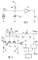
- An elementary integrator circuit is shown in FIG. 1. It includes an integration capacitor C int , a switch I a and a follower circuit S.
- the detected charges constitute a current Iph which is integrated in the capacitor C int .
- the switch I a makes it possible to reset the potential of the read node by application of a reset voltage V r .
- the follower circuit S delivers a voltage variation V s proportional to the current Iph.
- the maximum admissible photonic current Iph max the time Ti of integration of the charges in the capacitor C int and the integration capacitor C int verify the relationship: ph max x Ti ⁇ .DELTA.V S max G x C int where ⁇ V Smax is the maximum voltage excursion at the output of the follower S and G the voltage gain of the follower.
- the gain G will be taken equal to 1 which is the theoretical value of the gain of a voltage follower.
- the input excursion is substantially equal to 1/32, knowing that the signal-to-noise ratio of the photodiode is degraded by 2 under minimum lighting.
- the invention makes it possible to respond advantageously to this need.
- the invention relates to a charge reading circuit comprising a capacitive means of capacity C a for storing charges and means for reading a voltage taken from the terminals of the capacitive means.
- the capacitive means consists of a first capacitive means and a second capacitive means of capacity C b less than C a .
- the reading circuit comprises comparison means for comparing the voltage read across the terminals of the capacitive means with a threshold value, means for controlling the transfer of the charges stored in the first capacitive means to the second capacitive means of capacity C b less than C a when the voltage read across the capacitive means crosses the threshold value and means for reading a voltage drawn across the second capacitive means.
- the invention also relates to a method for reading charges comprising a step of integrating charges into a capacitive means of capacitance C a and a step of reading a voltage across the terminals of the capacitive means.
- the capacitive means consists of a first capacitive means and a second capacitive means of capacity C b less than C a .
- the method comprises, successively, a step of comparing the voltage read across the terminals of the capacitive means with a threshold voltage, a step of transferring the charges stored in the first capacitive means to the second capacitive means of capacity C b less than C a when the voltage read across the capacitive means crosses the threshold value, and a step of reading a voltage across the second capacitive means.
- the invention also relates to a circuit radiation detector comprising at least one photodetector to convert electrical charges into a detected radiation and a circuit for reading electrical charges.
- Load reading circuit electric is a charge reading circuit according to the invention.
- Figure 2 shows an integrator circuit elementary follower type according to a first mode of realization of the invention.
- the elementary integrator circuit includes two transistors of MOS technology T1 and T2 (MOS for “Metal Oxide Semiconductor”), three switches I1, I2, I3, a transistor TS mounted as a voltage follower, a comparator COMP and a control means CONT.
- the integrator circuit is connected to a detector consisting of a photodiode D and a direct injection MOS transistor T id controlled on its gate by a voltage ⁇ id .
- the two transistors T1 and T2 are connected in series.
- the drain of the transistor Tid drives the channel of the transistors T1 and T2.
- the transistor TS has its source connected to a column bus BC by means of the switch I3.
- the column bus BC is connected to a processing circuit CT.
- the switch I2 makes it possible to reset the potential V n of the read node to a reset voltage Vr.
- the comparator COMP has a first input connected, via the switch I3, to the output of the transistor TS and a second input connected to a voltage source V Threshold .
- the comparator output is connected, via switch I1, to CONT control.
- the switch I1 is controlled by a voltage V.
- the control means CONT carries the gate of the transistor T1 to a potential ⁇ c .
- the transistor T1 is then polarized in integration capacity C1 and the integration of the charges is also carried out in the transistor T2 which is polarized in integration capacity C2. Capacities C1 and C2 are in parallel.
- the integrator circuit allows integration of the current in the channel of the MOS transistors T1 and T2 which constitute the capacitors C1 and C2.
- the potential V n of the read node evolves as a function of time as described in FIG. 3 (A) or FIG. 3 (B) depending on whether the detected current Iph is a high current or a low current.
- high current is meant a current Iph such that at the end of the integration time Ti, the output voltage of the follower TS is less than the threshold voltage V Threshold .
- low current it is meant a current Iph such that at the end of the integration time Ti, the output voltage of the follower TS is greater than the threshold voltage V Threshold .
- the voltage ⁇ V 1 is then sampled and multiplexed to the video output.
- the comparator switches at an instant ta (cf. FIG. 3 (C)) and the signal which it delivers controls the CONT control means so as to apply a falling edge on the grid of T1 (cf. figure 3 (D)).
- the charges stored in the channel of T1 are then injected into the channel of T2 between the instants ta and tb.
- the voltage response of the elementary reading circuit is therefore advantageously multiplied by the factor VS 1 + C 2 VS 2 .
- this factor is at least equal to 5.
- the noise due to the transistor TS is divided by this same factor.
- the fact that the voltage response of the integrator circuit increases at low current allows, if necessary, reduce the requirements on the input noise of the multiplexing chain downstream.
- the comparison signal S COMP delivered by the comparator makes it possible to know the capacity on which the measurement of the charges was carried out.
- the comparison signal S COMP coupled to the voltage measurement read then makes it possible to calculate the value of the charge detected by the detector D.
- the integrator circuit includes two MOS transistors in series T1 and T2.
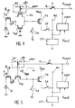
- Other embodiments of the invention are also possible, such as the modes shown in Figures 4 and 5.
- the means for storing the detected charges are capacities C3 and C4 connected in parallel respectively made using MOS transistors T11 and T22 mounted in parallel.
- the LAD control means the gate of transistor T11 and transistor T22 is polarized in integration capacity.
- the means of storage of detected charges are C5 capacities and C6 connected in parallel respectively carried out at using a MOS transistor T12 and a capacitor fixed value.
- the gate of transistor T12 is controlled by means of CONT control.
- the integrator circuit according to the invention can be implemented using different technologies.
- the photodiode can thus be connected by balls, via a device impedance matching, to the integration channel. She can also be performed on the integrated circuit of reading (N or P diode for detection in the visible).
- MOS transistors can be, for example, made on the same active layer (CMOS BULK or standard SOI) or on different layers active transferred to each other by techniques molecular adhesion type.
Landscapes
- Engineering & Computer Science (AREA)
- Multimedia (AREA)
- Signal Processing (AREA)
- Transforming Light Signals Into Electric Signals (AREA)
Abstract
Description
- la figure 1 représente un circuit intégrateur élémentaire de type suiveur selon l'art antérieur,
- la figure 2 représente un circuit intégrateur élémentaire de type suiveur selon un premier mode de réalisation de l'invention,
- la figure 3 représente des chronogrammes relatifs au fonctionnement du circuit intégrateur de type suiveur de la figure 2,
- la figure 4 représente un circuit intégrateur élémentaire de type suiveur selon un deuxième mode de réalisation de l'invention,
- la figure 5 représente un circuit intégrateur élémentaire de type suiveur selon un troisième mode de réalisation de l'invention.
Claims (10)
- Circuit de lecture de charges comprenant un moyen capacitif (C1, C2) de capacité Ca pour stocker des charges et des moyens pour lire une tension prélevée aux bornes du moyen capacitif, caractérisé en ce que le moyen capacitif étant constitué d'un premier moyen capacitif (C1) et d'un deuxième moyen capacitif (C2) de capacité Cb inférieure à Ca, il comprend des moyens de comparaison (COMP) pour comparer la tension lue aux bornes du moyen capacitif à une valeur de seuil (Vseuil), des moyens pour commander le transfert des charges stockées dans le premier moyen capacitif (C1) vers le deuxième moyen (C2) capacitif de capacité Cb inférieure à Ca lorsque la tension lue aux bornes du moyen capacitif franchit la valeur de seuil (Vseuil) et des moyens pour lire une tension prélevée aux bornes du deuxième moyen capacitif.
- Circuit de lecture selon la revendication 1, caractérisé en ce que le moyen capacitif comprend un premier transistor MOS.
- Circuit de lecture selon la revendication 2, caractérisé en ce que le moyen capacitif comprend un deuxième transistor MOS en série avec le premier transistor MOS, le deuxième transistor MOS constituant le deuxième moyen capacitif.
- Circuit de lecture selon la revendication 2, caractérisé en ce que le moyen capacitif comprend un deuxième transistor MOS en parallèle avec le premier transistor MOS, le deuxième transistor MOS constituant le deuxième moyen capacitif.
- Circuit de lecture selon la revendication 2, caractérisé en ce que le deuxième moyen capacitif est un condensateur de valeur fixe (C6).
- Circuit de lecture selon l'une quelconque des revendications précédentes, caractérisé en ce que les moyens pour lire une tension prélevée aux bornes du moyen capacitif constituent les moyens pour lire une tension prélevée aux bornes du deuxième moyen capacitif.
- Circuit de lecture selon l'une quelconque des revendications précédentes, caractérisé en ce que les moyens pour lire une tension prélevée aux bornes du moyen capacitif comprennent un suiveur de tension (TS).
- Circuit détecteur de rayonnement comprenant au moins un photodétecteur (D) pour convertir en charges électriques un rayonnement détecté et un circuit de lecture des charges électriques, caractérisé en ce que le circuit de lecture des charges électriques est un circuit de lecture de charges selon l'une quelconque des revendications précédentes.
- Procédé de lecture de charges comprenant une étape d'intégration de charges dans un moyen capacitif (C1, C2) de capacité Ca et une étape de lecture d'une tension aux bornes du moyen capacitif, caractérisé en ce que, le moyen capacitif étant constitué d'un premier moyen capacitif (C1) et d'un deuxième moyen capacitif (C2) de capacité Cb inférieure à Ca, il comprend, successivement, une étape de comparaison de la tension lue aux bornes du moyen capacitif avec une tension de seuil (Vseuil), une étape de transfert des charges stockées dans le premier moyen capacitif vers le deuxième moyen capacitif de capacité Cb inférieure à Ca lorsque la tension lue aux bornes du moyen capacitif franchit la valeur de seuil (Vseuil), et une étape de lecture d'une tension aux bornes du deuxième moyen capacitif.
- Procédé de lecture de charges selon la revendication 9, caractérisé en ce qu'il comprend une étape pour mesurer la valeur des charges intégrées dans le moyen capacitif à partir d'une valeur de tension de comparaison issue de l'étape de comparaison et de la valeur de tension lue.
Applications Claiming Priority (2)
| Application Number | Priority Date | Filing Date | Title |
|---|---|---|---|
| FR0016316A FR2818482B1 (fr) | 2000-12-14 | 2000-12-14 | Circuit de lecture de charges a preamplification adaptative et procede de lecture de charges a preamplification adaptative |
| FR0016316 | 2000-12-14 |
Publications (1)
| Publication Number | Publication Date |
|---|---|
| EP1215891A1 true EP1215891A1 (fr) | 2002-06-19 |
Family
ID=8857657
Family Applications (1)
| Application Number | Title | Priority Date | Filing Date |
|---|---|---|---|
| EP01403217A Withdrawn EP1215891A1 (fr) | 2000-12-14 | 2001-12-12 | Circuit de lecture de charges a préamplification adaptive et procédé de lecture des charges a préamplification adaptive |
Country Status (3)
| Country | Link |
|---|---|
| US (1) | US6603109B2 (fr) |
| EP (1) | EP1215891A1 (fr) |
| FR (1) | FR2818482B1 (fr) |
Families Citing this family (5)
| Publication number | Priority date | Publication date | Assignee | Title |
|---|---|---|---|---|
| US7671460B2 (en) * | 2006-01-25 | 2010-03-02 | Teledyne Licensing, Llc | Buried via technology for three dimensional integrated circuits |
| US7436342B2 (en) * | 2007-01-30 | 2008-10-14 | Teledyne Licensing, Llc | Numerical full well capacity extension for photo sensors with an integration capacitor in the readout circuit using two and four phase charge subtraction |
| US7923763B2 (en) * | 2007-03-08 | 2011-04-12 | Teledyne Licensing, Llc | Two-dimensional time delay integration visible CMOS image sensor |
| US7498650B2 (en) * | 2007-03-08 | 2009-03-03 | Teledyne Licensing, Llc | Backside illuminated CMOS image sensor with pinned photodiode |
| US7795650B2 (en) * | 2008-12-09 | 2010-09-14 | Teledyne Scientific & Imaging Llc | Method and apparatus for backside illuminated image sensors using capacitively coupled readout integrated circuits |
Citations (2)
| Publication number | Priority date | Publication date | Assignee | Title |
|---|---|---|---|---|
| US5742058A (en) * | 1995-06-14 | 1998-04-21 | Commissariat A L'energie Atomique | Device and a method of digitalization for photosensitive detectors and a method of reading a matrix of photonic detectors |
| GB2330905A (en) * | 1997-11-03 | 1999-05-05 | Hewlett Packard Co | Photodiode pixel sensor with switched shunt capacitance |
Family Cites Families (2)
| Publication number | Priority date | Publication date | Assignee | Title |
|---|---|---|---|---|
| US4965686A (en) | 1989-03-31 | 1990-10-23 | Raymond Engineering Inc. | Disc drive assembly for magnetic disc memory unit |
| US6104020A (en) * | 1998-02-17 | 2000-08-15 | Agilent Technologies | Electronic shutter for a low differential light level photo-receiver cell |
-
2000
- 2000-12-14 FR FR0016316A patent/FR2818482B1/fr not_active Expired - Fee Related
-
2001
- 2001-11-28 US US09/994,622 patent/US6603109B2/en not_active Expired - Fee Related
- 2001-12-12 EP EP01403217A patent/EP1215891A1/fr not_active Withdrawn
Patent Citations (2)
| Publication number | Priority date | Publication date | Assignee | Title |
|---|---|---|---|---|
| US5742058A (en) * | 1995-06-14 | 1998-04-21 | Commissariat A L'energie Atomique | Device and a method of digitalization for photosensitive detectors and a method of reading a matrix of photonic detectors |
| GB2330905A (en) * | 1997-11-03 | 1999-05-05 | Hewlett Packard Co | Photodiode pixel sensor with switched shunt capacitance |
Also Published As
| Publication number | Publication date |
|---|---|
| US20020109098A1 (en) | 2002-08-15 |
| US6603109B2 (en) | 2003-08-05 |
| FR2818482B1 (fr) | 2003-01-17 |
| FR2818482A1 (fr) | 2002-06-21 |
Similar Documents
| Publication | Publication Date | Title |
|---|---|---|
| EP0237365A1 (fr) | Dispositif photosensible | |
| EP2525406B1 (fr) | Circuit de détection à faible flux et faible bruit | |
| EP0743753A1 (fr) | Module interrupteur et d'alimentation | |
| EP0022015B1 (fr) | Dispositif amplificateur et procédé d'amplification pour audio-fréquences | |
| EP1215891A1 (fr) | Circuit de lecture de charges a préamplification adaptive et procédé de lecture des charges a préamplification adaptive | |
| FR2667471A1 (fr) | Dispositif pour prise de vues. | |
| EP0149948B1 (fr) | Perfectionnement aux dispositifs photosensibles à l'état solide | |
| FR2591409A1 (fr) | Camera thermique a balayage parallele | |
| EP0354106B1 (fr) | Circuit d'élimination du bruit, intégré dans un détecteur d'images à l'état solide | |
| EP0958545B1 (fr) | Circuit integrateur de charges photogenerees a linearite amelioree | |
| US12483809B2 (en) | Optical sensing system and analog-to-digital converter | |
| FR2705183A1 (fr) | Structure améliorée d'adressage à diodes pour adressage d'un réseau de transducteurs. | |
| EP0019506B1 (fr) | Dispositif à transfert de charges de soustraction et de génération de quantités de charges | |
| EP0021910A1 (fr) | Mosaique de détecteurs de rayonnement lue par un dispositif semiconducteur, et système de prise de vues comportant une telle mosaique | |
| FR2638309A1 (fr) | Plaquette de pretraitement des courants de sortie de diodes de detection soumises a un rayonnement thermique | |
| EP3114442A1 (fr) | Circuit de detection d'un rayonnement lumineux | |
| EP0654945A1 (fr) | Circuit d'injection, en imagerie thermique | |
| FR2730104A1 (fr) | Alimentation continue a correcteur de facteur de puissance et convertisseur a decoupage utilisable dans une telle alimentation | |
| FR2755323A1 (fr) | Dispositif de conversion analogique/numerique | |
| EP0146431B1 (fr) | Redresseur monoalternance a capacités commutées | |
| FR2754119A1 (fr) | Dispositif et procede de conversion de tension en rampe continue pour reseau neuronal | |
| FR2807601A1 (fr) | Dispositif de conversion d'un photosignal en tension dans les senseurs d'images a integrateurs deportes | |
| FR2755805A1 (fr) | Circuit d'amplification comprenant un dispositif de compensation de courant d'entree | |
| FR2737072A1 (fr) | Circuit de lecture de detecteurs de rayonnements electromagnetiques avec remise a zero du circuit de lecture par les detecteurs | |
| FR2818073A1 (fr) | Circuit de lecture de charges par calibration et procede de lecture de charges par calibration |
Legal Events
| Date | Code | Title | Description |
|---|---|---|---|
| PUAI | Public reference made under article 153(3) epc to a published international application that has entered the european phase |
Free format text: ORIGINAL CODE: 0009012 |
|
| AK | Designated contracting states |
Kind code of ref document: A1 Designated state(s): AT BE CH CY DE DK ES FI FR GB GR IE IT LI LU MC NL PT SE TR |
|
| AX | Request for extension of the european patent |
Free format text: AL;LT;LV;MK;RO;SI |
|
| RIN1 | Information on inventor provided before grant (corrected) |
Inventor name: ROTHAN, FREDERIC Inventor name: LAFLAQUIERE, ARNAUD C/O ST-MICROELECTRONICS Inventor name: PANTIGNY, PHILIPPE |
|
| 17P | Request for examination filed |
Effective date: 20021128 |
|
| AKX | Designation fees paid |
Designated state(s): DE GB IT |
|
| RAP1 | Party data changed (applicant data changed or rights of an application transferred) |
Owner name: COMMISSARIAT A L'ENERGIE ATOMIQUE |
|
| 17Q | First examination report despatched |
Effective date: 20061109 |
|
| RAP1 | Party data changed (applicant data changed or rights of an application transferred) |
Owner name: COMMISSARIAT A L'ENERGIE ATOMIQUE ET AUX ENERGIES |
|
| STAA | Information on the status of an ep patent application or granted ep patent |
Free format text: STATUS: THE APPLICATION IS DEEMED TO BE WITHDRAWN |
|
| 18D | Application deemed to be withdrawn |
Effective date: 20110701 |