EP1215717A1 - Magnetron plasma processing apparatus - Google Patents
Magnetron plasma processing apparatus Download PDFInfo
- Publication number
- EP1215717A1 EP1215717A1 EP00955070A EP00955070A EP1215717A1 EP 1215717 A1 EP1215717 A1 EP 1215717A1 EP 00955070 A EP00955070 A EP 00955070A EP 00955070 A EP00955070 A EP 00955070A EP 1215717 A1 EP1215717 A1 EP 1215717A1
- Authority
- EP
- European Patent Office
- Prior art keywords
- magnetic field
- anisotropic segment
- magnetron plasma
- segment magnets
- chamber
- Prior art date
- Legal status (The legal status is an assumption and is not a legal conclusion. Google has not performed a legal analysis and makes no representation as to the accuracy of the status listed.)
- Granted
Links
Images


Classifications
-
- H—ELECTRICITY
- H10—SEMICONDUCTOR DEVICES; ELECTRIC SOLID-STATE DEVICES NOT OTHERWISE PROVIDED FOR
- H10P—GENERIC PROCESSES OR APPARATUS FOR THE MANUFACTURE OR TREATMENT OF DEVICES COVERED BY CLASS H10
- H10P50/00—Etching of wafers, substrates or parts of devices
- H10P50/20—Dry etching; Plasma etching; Reactive-ion etching
- H10P50/24—Dry etching; Plasma etching; Reactive-ion etching of semiconductor materials
- H10P50/242—Dry etching; Plasma etching; Reactive-ion etching of semiconductor materials of Group IV materials
-
- H—ELECTRICITY
- H01—ELECTRIC ELEMENTS
- H01J—ELECTRIC DISCHARGE TUBES OR DISCHARGE LAMPS
- H01J37/00—Discharge tubes with provision for introducing objects or material to be exposed to the discharge, e.g. for the purpose of examination or processing thereof
- H01J37/32—Gas-filled discharge tubes
- H01J37/32431—Constructional details of the reactor
- H01J37/3266—Magnetic control means
-
- H—ELECTRICITY
- H01—ELECTRIC ELEMENTS
- H01J—ELECTRIC DISCHARGE TUBES OR DISCHARGE LAMPS
- H01J37/00—Discharge tubes with provision for introducing objects or material to be exposed to the discharge, e.g. for the purpose of examination or processing thereof
- H01J37/32—Gas-filled discharge tubes
- H01J37/34—Gas-filled discharge tubes operating with cathodic sputtering
- H01J37/3402—Gas-filled discharge tubes operating with cathodic sputtering using supplementary magnetic fields
- H01J37/3405—Magnetron sputtering
- H01J37/3408—Planar magnetron sputtering
Definitions
- the present invention relates to a magnetron plasma processing apparatus for processing a target substrate such as a semiconductor wafer with a magnetron plasma.
- a magnetron plasma etching apparatus for performing micropattern etching by generating a high-density plasma in a comparatively low-pressure atmosphere has been put into practical use.
- a permanent magnet is arranged above a chamber.
- the magnetic field produced by the permanent magnet is applied horizontally to a semiconductor wafer.
- An RF electric field perpendicular to the magnetic field is simultaneously applied to the semiconductor wafer.
- the drift motion of electrons caused upon application of the magnetic and electric fields is utilized to etch the semiconductor wafer with a very high efficiency.
- FIG. 9 is a view (plan view) of the apparatus seen from above.
- reference numeral 100 denotes a semiconductor wafer.
- the horizontal magnetic field formed by the dipole ring magnet in this manner is a horizontal magnetic field directed only in one direction of from N to S in FIG. 9. Accordingly, electrons travel in one direction by drift motion, causing nonuniformity in the plasma density. More specifically, the electrons drift in the direction of the outer product of the electric field and the magnetic field. In other words, when the electric field is formed to extend downward from above, the electrons travel from the E pole side to the W pole side by drift motion. Consequently, the plasma density is low on the E pole side and high in the W pole side, resulting in nonuniformity.
- the dipole ring magnet is rotated in its circumferential direction to form a rotating magnetic field, so the direction of drift motion of electrons is changed. In practice, however, this cannot make the plasma density sufficiently uniform over a wide range.
- the magnetic field strength may be increased.
- the magnetic field strength of that portion where a wafer is present is limited to about 200 Gauss at maximum. Even when a magnetic field gradient is formed by the above technique and plasma uniformity can be achieved, the plasma density cannot be sufficiently increased, and the etching rate may not be sufficiently high. If a region where the magnetic field is locally strong can be formed outside the E pole-side end of the wafer, the plasma density may be increased without damaging the wafer. Conventionally, however, it is difficult to locally form a strong magnetic field portion.
- a magnetron plasma processing apparatus which comprises a chamber with an outer wall that can maintain a reduced pressure, process gas supply means for supplying a process gas into the chamber, a pair of electrodes arranged in the chamber to oppose each other and to define a processing space therebetween, electric field forming means for applying a voltage to the pair of electrodes, thus forming an electric field in the processing space, and magnetic field forming means for forming, in the processing space, a magnetic field perpendicular to the direction of the electric field and directed in one direction, and which subjects a target substrate to a magnetron plasma process while the target substrate is set in the processing space to be parallel to the electrodes, the magnetic field forming means having a dipole ring magnet including a plurality of first anisotropic segment magnets arranged in a ring-like shape around the outer wall of the chamber so as to form a magnetic field gradient, within a plane perpendicular to the direction of the electric field, such that a magnetic field strength
- a magnetron plasma processing apparatus which comprises a chamber which has an outer wall and can maintain reduced pressure, process gas supply means for supplying a process gas into the chamber, a pair of electrodes arranged in the chamber to oppose each other and to define a processing space therebetween, electric field forming means for applying a voltage to the pair of electrodes, thus forming an electric field in the processing space, and magnetic field forming means for forming, in the processing space between the pair of electrodes, a magnetic field perpendicular to the direction of the electric field and directed in one direction, and which subjects a target substrate to a magnetron plasma process while the target substrate is set in the processing space to be parallel to the electrodes, the magnetic field forming means having a dipole ring magnet including a large number of anisotropic segment magnets arranged in a ring-like shape around the outer wall of the chamber, to form a magnetic field gradient, within a plane perpendicular to the direction of the electric field between the electrodes,
- a strong magnetic field portion can be locally formed at a predetermined region located outside that end of the target substrate which is on the upstream side in the electron drift direction.
- the plasma density of the processing space can accordingly be increased.
- the anisotropic segment magnets are arranged such that gaps among those which are on the upstream side in the electron drift direction are narrower than gaps among those which are on the downstream side in the electron drift direction.
- the anisotropic segment magnets preferably form a magnetic field with 200 Gauss at maximum, preferably 100 Gauss to 200 Gauss, at a portion thereof opposing the target substrate, and a magnetic field of at least 200 Gauss, preferably 200 Gauss to 400 Gauss, at the predetermined region.
- FIG. 1 is a sectional view showing a magnetron plasma etching apparatus according to an embodiment of the present invention.
- This etching apparatus has an airtight chamber 1.
- the chamber 1 forms a stepped cylindrical shape constituted by a small-diameter upper portion 1a and large-diameter lower portion 1b.
- the wall of the chamber 1 is made of a conductor such as aluminum.
- a support table 2 for horizontally supporting a semiconductor wafer 30 as a target object thereon is arranged in the chamber 1.
- the support table 2 is formed of an aluminum circular plate, and is supported on a conductive support base 4 through an insulating plate 3.
- the support table 2 and support base 4 can be vertically moved with respect to the chamber 1 by a known ball screw mechanism in directions indicated by arrows.
- the ball screw mechanism has at least one (two in this embodiment) ball screw 7 and a motor (not shown) for rotating the screw.
- a driving portion under the support base 4 is covered by a stainless steel (SUS) bellows 8 set between the support base 4 and the bottom wall of the chamber 1.
- a bellows cover 9 formed of a pair of slidable cylinders is arranged outside the bellows 8.
- the support table 2 is connected to an RF power supply 10 through a matching box, i.e., a circuit 11.
- the RF power supply 10 supplies RF power of, e.g., 13.56 MHz, to the support table 2.
- a shower head 16 (to be described later) is arranged above the support table 2 to oppose and be parallel to it.
- the shower head 16 makes up the upper portion of the small-diameter portion of the chamber 1.
- the shower head 16 is grounded.
- the shower head 16 and support table 2 serve as a pair of parallel electrodes.
- An electrostatic chuck 6 for electrostatically chucking the semiconductor wafer 30 with a diameter of 300 mm is arranged on the surface of the support table 2.
- the electrostatic chuck 6 is surrounded by the focus ring 5.
- the electrostatic chuck 6 is constituted by a pair of insulators 6b, and an electrode 6a interposed between them and connected to a DC power supply 12.
- the power supply 12 applies a voltage to the electrode 6a, so that the semiconductor wafer 30 can be chucked on the electrostatic chuck with a Coulomb force.
- a refrigerant channel (not shown) is formed in the support table 2.
- the semiconductor wafer 30 can be controlled to a predetermined temperature.
- a baffle plate 13 is formed outside the focus ring 5 and electrically connected to the chamber 1 through the support base 4 and bellows 8.
- the shower head 16 has a lower plate 16a with a large number of gas discharge holes 18.
- a gas inlet portion 16b is formed at the center of the upper wall of the chamber 1 which is located above the lower plate 16a.
- a space 17 is formed in the shower head, i.e., between the lower plate 16a and the upper wall.
- the gas inlet portion 16b is connected to one end of a gas supply pipe 15a.
- the other end of the gas supply pipe 15a is connected to a process gas supply system 15 for supplying a process gas.
- the process gas consists of an etching reaction gas and diluent gas.
- As the reaction gas a halogen-based gas can be used.
- diluent gas a gas ordinarily used in this field, e.g., Ar gas, He gas, or the like can be used.
- the process gas is supplied from the process gas supply system 15 through the gas supply pipe 15a and gas inlet portion 16b in the space 17 of the shower head 16, and then discharged from the gas discharge holes 18 to etch a film formed on the semiconductor wafer 30.
- An exhaust port 19 is formed in the side wall of the lower portion 1b of the chamber 1, and is connected to an exhaust system 20.
- a vacuum pump provided in the exhaust system 20 When actuated, the interior of the chamber 1 can be reduced to a predetermined vacuum degree.
- a gate valve 24 is provided on the upper side of the side wall of the lower portion 1b of the chamber 1. The gate valve 24 opens and closes a loading/unloading port for the semiconductor wafer 30.
- a dipole ring magnet 21 is concentrically arranged around the upper portion 1a of the chamber 1.
- the dipole ring magnet 21 forms a horizontal magnetic field in the processing space between the support table 2 and shower head 16.
- the dipole ring magnet 21 can be rotated by a rotating means such as a motor (not shown) about the central axis of the upper portion 1a as the center.
- the gate valve 24 is opened.
- the semiconductor wafer 30 is loaded into the chamber 1 and placed on the support table 2.
- the DC power supply 12 applies a predetermined voltage to the electrode 6a of the electrostatic chuck 6.
- the semiconductor wafer 30 is chucked on the electrostatic chuck with a Coulomb force.
- the support table 2 is moved upward to the position shown in FIG. 1.
- the vacuum pump of the exhaust system 20 evacuates the interior of the chamber 1 through the exhaust port 19.
- the RF power supply 10 supplies RF power to the support table 2.
- the RF power has a frequency of 13.56 MHz and a power of 1,000 W to 5,000 W.
- the RF power is applied in the above manner to the support table 2 serving as a lower electrode.
- a vertical electric field is formed in the processing space between the shower head 16 serving as the upper electrode and the support table 2 serving as the lower electrode.
- a horizontal magnetic field is formed in the upper portion 1a of the chamber 1 by the dipole ring magnet 21. Therefore, magnetron discharge occurs in the process gas due to the drift of electrons, thus forming a process gas plasma.
- the process gas plasma etches a predetermined film formed on the semiconductor wafer 30.
- the dipole ring magnet will be described.
- FIG. 2 is a cross-sectional view of the dipole ring magnet arranged around the chamber 1.
- the dipole ring magnet 21 is formed by attaching a large number of anisotropic segment magnets 22 to a ring-like magnetic casing 23.
- Each anisotropic segment magnet 22 is formed of a columnar magnet with a magnetizing direction in its radial direction. In this embodiment, 30 anisotropic segment magnets 22 are arranged in the ring-like shape.
- the number of anisotropic segment magnets is not limited to this.
- the sectional shape of each anisotropic segment magnet is not limited to a circle as in the embodiment, but an arbitrary shape can be employed, e.g., a square, rectangle, or trapezoid.
- the magnet material that forms the anisotropic segment magnets 22 is not limited particularly, and a known magnet material can be employed, e.g., a rare earth-type magnet, a ferrite-type magnet, or an Alnico magnet.
- a known magnet material can be employed, e.g., a rare earth-type magnet, a ferrite-type magnet, or an Alnico magnet.
- the arrangement of such a dipole ring magnet and the rotating mechanism for it are disclosed in, e.g., U.S.P. No. 6,014,943 described herein as a reference.
- the dipole ring magnet 21 has first-group first anisotropic segment magnets 22 that form a horizontal magnetic field B directed in one direction as a whole, as shown in FIG. 2.
- the proximal end side of the direction of the magnetic field is shown as an N pole side
- the distal end side thereof is shown as an S pole side
- positions shifted by 90° from the N and S end sides are respectively shown as E and W poles.
- a vertical electric field EL and the horizontal magnetic field B extending almost from the N pole side toward the S pole side are formed in the processing space.
- electrons generated by the plasma travel from the E pole side toward the W pole side by drift motion. Therefore, the electron density on the W side will increase to cause nonuniformity in plasma density.
- the larger the magnetic field strength the larger the plasma density.
- those anisotropic segment magnets which are on the W pole side portion are thinned out to be less than those on the E pole side. Also, the magnetic strength of the anisotropic segment magnets on the E pole side is increased. In this manner, the magnet is designed to form lines of magnetic force with which the magnetic field strength on the E pole side end of the processing space is largest and the drift electrons diffuse on the W pole side.
- the magnetic field strength must be set to 200 Gauss or less even at the E pole side end where it is largest on the semiconductor wafer 30, because of possible charge-up damage.
- the magnetic field strength outside the E pole side end of the wafer is not sufficiently large.
- the amount of generated plasma may decrease and the etching rate may not be sufficiently high.
- a plasma etching process under a lower pressure is required.
- the plasma density must be further increased.
- the conventional magnetic field gradient however, a sufficient amount of plasma cannot be generated.
- those anisotropic segment magnets which are on the W pole side portion are thinned out to decrease the magnetic field strength of the W pole side.
- the magnetic poles of the anisotropic segment magnets at portions indicated by reference numerals a and b in FIG. 2 in the vicinity of a region A are directed toward the region A .
- These anisotropic segment magnets are second and third anisotropic segment magnets. More specifically, in the anisotropic segment magnets at the portion a , the N poles are directed toward the region A . In the anisotropic segment magnets at the portion b , the S poles are directed toward the region A .
- the magnetic field of the region A can be locally strengthened.
- the magnetic field strength of a region outside the E pole side end of the semiconductor wafer 30 is increased in this manner, the amount of plasma generated at this region can be increased.
- the plasma density can be increased.
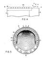
- the magnetic field strength of a region outside the E pole side of the semiconductor wafer 30 is increased to preferably 200 Gauss or more. Then, as shown in FIG. 4, the amount of electrons generated on the surface of the focus ring 5 outside the E side of the semiconductor wafer 30 increases. Thus, the amount of electrons to be supplied to the W side by drift increases, and accordingly the plasma density increases.
- FIG. 5 shows the magnetic field strength distribution formed when the magnetic poles of the anisotropic segment magnets at the portions indicated by a and b are directed to the region A according to the present invention, as shown in FIG. 2.
- FIG. 6 shows the magnetic field strength obtained when the directions of these magnetic poles are not changed.
- the isomagnetics are plotted at a spacing of 10 Gauss.
- a comparison of FIGS. 5 and 6 reveals the following.
- the spacings between the isomagnetics are dense at a portion (above the center) corresponding to the region A. The gradient of the magnetic field strength is thus steep, and the magnetic field strength is large at this portion.
- FIG. 5 shows the magnetic field strength distribution formed when the magnetic poles of the anisotropic segment magnets at the portions indicated by a and b are directed to the region A according to the present invention, as shown in FIG. 2.
- FIG. 6 shows the magnetic field strength obtained when the directions of these magnetic poles are not changed.
- the isomagnetics are plotted at
- the spacings between the isomagnetics at a portion corresponding to the region A are not very dense.
- the gradient of the magnetic field strength is thus moderate, and the magnetic field strength at this portion is not very large.
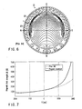
- An actual magnetic field strength gradient in an E - W section is as shown in FIG. 7.
- the gradient of the magnetic field strength is steep at a region outside the E side end of the semiconductor wafer 30, and a magnetic field strength considerably larger than that of the prior art can be obtained.
- a portion with a large magnetic field strength as described above is preferably formed over a wide range outside the E pole side of the semiconductor wafer 30.
- An isomagnetic strength may then be obtained over a wide range along the E pole side end of the semiconductor wafer 30 and its periphery. Then, electrons start drifting simultaneously over the wide range in the vicinity of the end region of the semiconductor wafer 30. Therefore, the plasma density can be increased easily.
- the magnetic pole of at least one (three in this example) anisotropic segment magnet of a portion c in the vicinity of the region C may be directed toward the region C .
- the magnetic pole of at least one (three in this example) anisotropic segment magnet of a portion d in the vicinity of the region D may be directed toward the region D .
- a desired magnetic field strength distribution can be obtained. More specifically, the N poles of the three anisotropic segment magnets at the portion c are directed toward the region C .
- the S poles of the three anisotropic segment magnets at the portion d are directed toward the region D .
- the N and S poles of the anisotropic segment magnets are directed toward the regions C and D , respectively. Then, in these regions, of the magnetic fields formed by the dipole ring magnet, those of the regions C and D can be locally strengthened.
- the present invention is not limited to the above embodiments but can be changed in various ways.
- a semiconductor wafer with an oxide film is used as a target substrate.
- the present invention is not limited to this, and other target substrates, e.g., an LCD substrate or a glass substrate with an insulating film, may be used.
- the present invention is applied to a magnetron plasma etching apparatus.
- the present invention is not limited to this, but can be applied to another plasma processing apparatus.
- the technique of decreasing the magnetic field strength on the W pole side so that it is smaller than that on the E pole side is not limited to changing the numbers of anisotropic segment magnets on the two pole sides, as described above. It is understood that another means can be used.
- the numbers of anisotropic segment magnets are set equal, while the magnetic strengths thereof are made to differ. Furthermore, regarding the number of anisotropic segment magnets arranged in order to locally increase the magnetic field of a predetermined region, at least one suffices. This number can be arbitrarily selected.
- This anisotropic segment magnet need not have the same shape and characteristics as those of other anisotropic segment magnets. Also, this anisotropic segment magnet need not be positioned on the same circle where other ones are placed.
- the upper electrode is formed by a shower head.
- the upper electrode may be a mere plate-like electrode.
- a port through which the process gas is to be introduced may be formed at another location, e.g., in the outer wall of the chamber, and the process gas may be directly supplied into the processing space.
- the target substrate can be arranged such that it is supported by the upper electrode.
- a magnetic field forming means can form a strong magnetic field portion locally at a predetermined region located outside that end of a target substrate which is upstream in the electron drift direction.
- the plasma density of the processing space can accordingly be increased.
- the apparatus of the present invention is used as, e.g., an etching apparatus, uniform etching can be performed under a low pressure.
- the present invention is thus suitable for etching a device that needs to be micropatterned.
Landscapes
- Physics & Mathematics (AREA)
- Engineering & Computer Science (AREA)
- Plasma & Fusion (AREA)
- Chemical & Material Sciences (AREA)
- Analytical Chemistry (AREA)
- Drying Of Semiconductors (AREA)
- Plasma Technology (AREA)
- ing And Chemical Polishing (AREA)
Abstract
Description
- The present invention relates to a magnetron plasma processing apparatus for processing a target substrate such as a semiconductor wafer with a magnetron plasma.
- In recent years, a magnetron plasma etching apparatus for performing micropattern etching by generating a high-density plasma in a comparatively low-pressure atmosphere has been put into practical use. In this apparatus, a permanent magnet is arranged above a chamber. The magnetic field produced by the permanent magnet is applied horizontally to a semiconductor wafer. An RF electric field perpendicular to the magnetic field is simultaneously applied to the semiconductor wafer. The drift motion of electrons caused upon application of the magnetic and electric fields is utilized to etch the semiconductor wafer with a very high efficiency.
- In the magnetron plasma, what contributes to the drift motion of electrons is a magnetic field perpendicular to the electric field, i.e., a magnetic field horizontal to the semiconductor wafer. As a uniform horizontal magnetic field is not always formed in the above apparatus, plasma uniformity is not sufficient. Thus, a nonuniform etching rate, charge-up damage, and the like may occur.
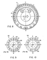
- In order to avoid these problems, formation of a horizontal magnetic field uniform with respect to the semiconductor wafer in the processing space in the chamber is sought. As a magnet that can generate such a magnetic field, a dipole ring magnet is known. As shown in FIG. 9, this
dipole ring magnet 102 is formed by arranging a plurality of anisotropic segmentcolumnar magnets 103 in a ring-like shape outside achamber 101. The directions of magnetization of the plurality of anisotropic segmentcolumnar magnets 103 are slightly shifted from each other to form a uniform horizontal magnetic field B as a whole. FIG. 9 is a view (plan view) of the apparatus seen from above. The proximal end side of the direction of the magnetic field is indicated by N, the distal end side thereof is indicated by S, and positions separated 90° from N and S are respectively indicated by E and W. In FIG. 9,reference numeral 100 denotes a semiconductor wafer. - The horizontal magnetic field formed by the dipole ring magnet in this manner is a horizontal magnetic field directed only in one direction of from N to S in FIG. 9. Accordingly, electrons travel in one direction by drift motion, causing nonuniformity in the plasma density. More specifically, the electrons drift in the direction of the outer product of the electric field and the magnetic field. In other words, when the electric field is formed to extend downward from above, the electrons travel from the E pole side to the W pole side by drift motion. Consequently, the plasma density is low on the E pole side and high in the W pole side, resulting in nonuniformity.
- To prevent this, the dipole ring magnet is rotated in its circumferential direction to form a rotating magnetic field, so the direction of drift motion of electrons is changed. In practice, however, this cannot make the plasma density sufficiently uniform over a wide range.
- A technique has been proposed in which a magnetic field gradient is formed in the drift direction of electrons, i.e., in a direction from the E pole side to the W pole side in FIG. 9, so the nonuniformity of plasma accompanying the drift motion of electrons is eliminated (Jpn. Pat. Appln. KOKAI Publication No. 9-27278). According to this technique, as shown in FIG. 10, the number of anisotropic segment columnar magnets on the W pole side is made smaller than that on the E pole side. As a result, a gradient is formed in which the magnetic field strength increases in the direction from the E pole side to the W pole side.
- In recent years, devices have been required to shrink more and more in feature size, and a plasma etching process in a lower pressure has been required. To perform an efficient plasma process in a low pressure, the plasma density must be further increased. For this purpose, in the magnetron plasma process, the magnetic field strength may be increased.
- When, however, an insulating film such as an oxide film is to be etched, to avoid charge-up damage, the magnetic field strength of that portion where a wafer is present is limited to about 200 Gauss at maximum. Even when a magnetic field gradient is formed by the above technique and plasma uniformity can be achieved, the plasma density cannot be sufficiently increased, and the etching rate may not be sufficiently high. If a region where the magnetic field is locally strong can be formed outside the E pole-side end of the wafer, the plasma density may be increased without damaging the wafer. Conventionally, however, it is difficult to locally form a strong magnetic field portion.
- It is an object of the present invention to provide a magnetron plasma processing apparatus which can form a locally strong magnetic field portion at a desired position in a processing space for a target object, so the plasma density of the processing space can be increased.
- According to a first aspect of the present invention, there is provided a magnetron plasma processing apparatus which comprises
a chamber with an outer wall that can maintain a reduced pressure,
process gas supply means for supplying a process gas into the chamber,
a pair of electrodes arranged in the chamber to oppose each other and to define a processing space therebetween,
electric field forming means for applying a voltage to the pair of electrodes, thus forming an electric field in the processing space, and
magnetic field forming means for forming, in the processing space, a magnetic field perpendicular to the direction of the electric field and directed in one direction, and which subjects a target substrate to a magnetron plasma process while the target substrate is set in the processing space to be parallel to the electrodes,
the magnetic field forming means having a dipole ring magnet including a plurality of first anisotropic segment magnets arranged in a ring-like shape around the outer wall of the chamber so as to form a magnetic field gradient, within a plane perpendicular to the direction of the electric field, such that a magnetic field strength is large and small on upstream and downstream sides, respectively, in an electron drift direction along a direction perpendicular to a direction of the magnetic field,
at least one second anisotropic segment magnet, arranged in the vicinity of a predetermined region located outside that end of the target substrate which is on the upstream side in the electron drift direction, with an N pole thereof being directed toward the predetermined region, and
at least one third anisotropic segment magnet arranged in the vicinity of the predetermined region with an S pole thereof being directed toward the predetermined region,
the second and third anisotropic segment magnets serving to locally increase the magnetic field strength of the predetermined region to be larger than that formed by the first anisotropic segment magnets. - According to a second aspect of the present invention, there is provided a magnetron plasma processing apparatus which comprises
a chamber which has an outer wall and can maintain reduced pressure,
process gas supply means for supplying a process gas into the chamber,
a pair of electrodes arranged in the chamber to oppose each other and to define a processing space therebetween,
electric field forming means for applying a voltage to the pair of electrodes, thus forming an electric field in the processing space, and
magnetic field forming means for forming, in the processing space between the pair of electrodes, a magnetic field perpendicular to the direction of the electric field and directed in one direction, and which subjects a target substrate to a magnetron plasma process while the target substrate is set in the processing space to be parallel to the electrodes,
the magnetic field forming means having a dipole ring magnet including a large number of anisotropic segment magnets arranged in a ring-like shape around the outer wall of the chamber, to form a magnetic field gradient, within a plane perpendicular to the direction of the electric field between the electrodes, such that the magnetic field strength is large and small on upstream and downstream sides, respectively, in an electron drift direction along a direction perpendicular to the direction of the magnetic field, and
the plurality of anisotropic segment magnets including a first portion including at least one anisotropic segment magnet arranged in the vicinity of a first region located outside that end of the target substrate which is on the upstream side in the electron drift direction with an N pole thereof being directed toward the first region, and a second portion including at least one anisotropic segment magnet, arranged in the vicinity of a second region located outside that end of the target substrate which is on the upstream side in the electron drift direction, to be away from the first region, with an S pole thereof being directed toward the second region, the first and second portions serving to locally increase magnetic field strengths of the first and second regions. - With the above arrangement, a strong magnetic field portion can be locally formed at a predetermined region located outside that end of the target substrate which is on the upstream side in the electron drift direction. The plasma density of the processing space can accordingly be increased.
- Preferably, the anisotropic segment magnets are arranged such that gaps among those which are on the upstream side in the electron drift direction are narrower than gaps among those which are on the downstream side in the electron drift direction.
- The anisotropic segment magnets preferably form a magnetic field with 200 Gauss at maximum, preferably 100 Gauss to 200 Gauss, at a portion thereof opposing the target substrate, and a magnetic field of at least 200 Gauss, preferably 200 Gauss to 400 Gauss, at the predetermined region.
-
- FIG. 1 is a sectional view showing a magnetron plasma etching apparatus according to an embodiment of the present invention;
- FIG. 2 is a horizontal sectional view of a dipole ring magnet arranged around the chamber of the apparatus of FIG. 1;
- FIG. 3 is a view schematically showing the dipole ring magnet and a state in the chamber of the magnetron plasma etching apparatus of FIG. 1;
- FIG. 4 is a schematic view showing the drift state of electrons generated by a focus ring in the magnetron plasma etching apparatus according to the embodiment of the present invention;
- FIG. 5 is a view showing the magnetic field strength distribution of a magnetic field formed by the dipole ring magnet of FIG. 2;
- FIG. 6 is a view showing the magnetic field strength distribution of a magnetic field formed by a conventional dipole ring magnet;
- FIG. 7 is a graph showing the magnetic field strength gradient in the E - W section of the processing space of the magnetron plasma etching apparatus according to the present invention and that of a conventional magnetron plasma etching apparatus;
- FIG. 8 is a horizontal sectional view of a dipole ring magnet arranged around the chamber of a magnetron plasma etching apparatus according to another embodiment of the present invention;
- FIG. 9 is a schematic view showing a conventional dipole ring magnet; and
- FIG. 10 is a schematic view showing a conventional dipole ring magnet.
-
- The embodiments of the present invention will be described with reference to the accompanying drawings.
- FIG. 1 is a sectional view showing a magnetron plasma etching apparatus according to an embodiment of the present invention. This etching apparatus has an
airtight chamber 1. Thechamber 1 forms a stepped cylindrical shape constituted by a small-diameter upper portion 1a and large-diameter lower portion 1b. The wall of thechamber 1 is made of a conductor such as aluminum. A support table 2 for horizontally supporting asemiconductor wafer 30 as a target object thereon is arranged in thechamber 1. For example, the support table 2 is formed of an aluminum circular plate, and is supported on aconductive support base 4 through an insulating plate 3. Aconductive focus ring 5 made of, e.g., single-crystal silicon, is arranged on the periphery of an upper surface of the support table 2. The support table 2 andsupport base 4 can be vertically moved with respect to thechamber 1 by a known ball screw mechanism in directions indicated by arrows. The ball screw mechanism has at least one (two in this embodiment) ball screw 7 and a motor (not shown) for rotating the screw. A driving portion under thesupport base 4 is covered by a stainless steel (SUS) bellows 8 set between thesupport base 4 and the bottom wall of thechamber 1. A bellows cover 9 formed of a pair of slidable cylinders is arranged outside the bellows 8. - The support table 2 is connected to an
RF power supply 10 through a matching box, i.e., acircuit 11. TheRF power supply 10 supplies RF power of, e.g., 13.56 MHz, to the support table 2. A shower head 16 (to be described later) is arranged above the support table 2 to oppose and be parallel to it. Theshower head 16 makes up the upper portion of the small-diameter portion of thechamber 1. Theshower head 16 is grounded. Thus, theshower head 16 and support table 2 serve as a pair of parallel electrodes. - An
electrostatic chuck 6 for electrostatically chucking thesemiconductor wafer 30 with a diameter of 300 mm is arranged on the surface of the support table 2. Theelectrostatic chuck 6 is surrounded by thefocus ring 5. Theelectrostatic chuck 6 is constituted by a pair ofinsulators 6b, and an electrode 6a interposed between them and connected to aDC power supply 12. Thepower supply 12 applies a voltage to the electrode 6a, so that thesemiconductor wafer 30 can be chucked on the electrostatic chuck with a Coulomb force. - A refrigerant channel (not shown) is formed in the support table 2. When an appropriate refrigerant is circulated in the refrigerant channel, the
semiconductor wafer 30 can be controlled to a predetermined temperature. Abaffle plate 13 is formed outside thefocus ring 5 and electrically connected to thechamber 1 through thesupport base 4 and bellows 8. - The
shower head 16 has a lower plate 16a with a large number of gas discharge holes 18. Agas inlet portion 16b is formed at the center of the upper wall of thechamber 1 which is located above the lower plate 16a. Aspace 17 is formed in the shower head, i.e., between the lower plate 16a and the upper wall. Thegas inlet portion 16b is connected to one end of a gas supply pipe 15a. The other end of the gas supply pipe 15a is connected to a processgas supply system 15 for supplying a process gas. The process gas consists of an etching reaction gas and diluent gas. As the reaction gas, a halogen-based gas can be used. As the diluent gas, a gas ordinarily used in this field, e.g., Ar gas, He gas, or the like can be used. - The process gas is supplied from the process
gas supply system 15 through the gas supply pipe 15a andgas inlet portion 16b in thespace 17 of theshower head 16, and then discharged from the gas discharge holes 18 to etch a film formed on thesemiconductor wafer 30. - An
exhaust port 19 is formed in the side wall of the lower portion 1b of thechamber 1, and is connected to anexhaust system 20. When a vacuum pump provided in theexhaust system 20 is actuated, the interior of thechamber 1 can be reduced to a predetermined vacuum degree. Agate valve 24 is provided on the upper side of the side wall of the lower portion 1b of thechamber 1. Thegate valve 24 opens and closes a loading/unloading port for thesemiconductor wafer 30. - A
dipole ring magnet 21 is concentrically arranged around the upper portion 1a of thechamber 1. Thedipole ring magnet 21 forms a horizontal magnetic field in the processing space between the support table 2 andshower head 16. Thedipole ring magnet 21 can be rotated by a rotating means such as a motor (not shown) about the central axis of the upper portion 1a as the center. - In the magnetron plasma etching apparatus with the above arrangement, first, the
gate valve 24 is opened. Thesemiconductor wafer 30 is loaded into thechamber 1 and placed on the support table 2. At this time, theDC power supply 12 applies a predetermined voltage to the electrode 6a of theelectrostatic chuck 6. Thesemiconductor wafer 30 is chucked on the electrostatic chuck with a Coulomb force. After this, the support table 2 is moved upward to the position shown in FIG. 1. The vacuum pump of theexhaust system 20 evacuates the interior of thechamber 1 through theexhaust port 19. - After the interior of the
chamber 1 reaches the predetermined vacuum degree, a predetermined process gas is introduced into thechamber 1 from the processgas supply system 15. The interior of thechamber 1 is thus held at a predetermined pressure, e.g., 50 mTorr. In this state, theRF power supply 10 supplies RF power to the support table 2. For example, the RF power has a frequency of 13.56 MHz and a power of 1,000 W to 5,000 W. - In this case, the RF power is applied in the above manner to the support table 2 serving as a lower electrode. Thus, a vertical electric field is formed in the processing space between the
shower head 16 serving as the upper electrode and the support table 2 serving as the lower electrode. A horizontal magnetic field is formed in the upper portion 1a of thechamber 1 by thedipole ring magnet 21. Therefore, magnetron discharge occurs in the process gas due to the drift of electrons, thus forming a process gas plasma. The process gas plasma etches a predetermined film formed on thesemiconductor wafer 30. - The dipole ring magnet will be described.
- FIG. 2 is a cross-sectional view of the dipole ring magnet arranged around the
chamber 1. - As shown in FIG. 2, the
dipole ring magnet 21 is formed by attaching a large number ofanisotropic segment magnets 22 to a ring-likemagnetic casing 23. Eachanisotropic segment magnet 22 is formed of a columnar magnet with a magnetizing direction in its radial direction. In this embodiment, 30anisotropic segment magnets 22 are arranged in the ring-like shape. However, the number of anisotropic segment magnets is not limited to this. The sectional shape of each anisotropic segment magnet is not limited to a circle as in the embodiment, but an arbitrary shape can be employed, e.g., a square, rectangle, or trapezoid. The magnet material that forms theanisotropic segment magnets 22 is not limited particularly, and a known magnet material can be employed, e.g., a rare earth-type magnet, a ferrite-type magnet, or an Alnico magnet. The arrangement of such a dipole ring magnet and the rotating mechanism for it are disclosed in, e.g., U.S.P. No. 6,014,943 described herein as a reference. - In the
dipole ring magnet 21, the directions of magnetization of the plurality of first-group firstanisotropic segment magnets 22 are slightly shifted from each other in the same manner as in the prior art. Thus, thedipole ring magnet 21 has first-group firstanisotropic segment magnets 22 that form a horizontal magnetic field B directed in one direction as a whole, as shown in FIG. 2. In FIG. 2, the proximal end side of the direction of the magnetic field is shown as an N pole side, the distal end side thereof is shown as an S pole side, and positions shifted by 90° from the N and S end sides are respectively shown as E and W poles. - As shown in FIG. 3, a vertical electric field EL and the horizontal magnetic field B extending almost from the N pole side toward the S pole side are formed in the processing space. Thus, electrons generated by the plasma travel from the E pole side toward the W pole side by drift motion. Therefore, the electron density on the W side will increase to cause nonuniformity in plasma density. The larger the magnetic field strength, the larger the plasma density. When a magnetic field strength gradient is formed such that the magnetic field strength on the E pole side is large and that on the W pole side is small, the above problem can be solved.
- For this purpose, conventionally, those anisotropic segment magnets which are on the W pole side portion are thinned out to be less than those on the E pole side. Also, the magnetic strength of the anisotropic segment magnets on the E pole side is increased. In this manner, the magnet is designed to form lines of magnetic force with which the magnetic field strength on the E pole side end of the processing space is largest and the drift electrons diffuse on the W pole side.
- When the insulating film (oxide film, nitride film, or the like) on the
semiconductor wafer 30 is to be etched, the magnetic field strength must be set to 200 Gauss or less even at the E pole side end where it is largest on thesemiconductor wafer 30, because of possible charge-up damage. With a conventional magnetic gradient, the magnetic field strength outside the E pole side end of the wafer is not sufficiently large. Hence, the amount of generated plasma may decrease and the etching rate may not be sufficiently high. In other words, as the feature size of the devices shrinks in recent years, a plasma etching process under a lower pressure is required. To perform an efficient plasma process under a low pressure, the plasma density must be further increased. With the conventional magnetic field gradient, however, a sufficient amount of plasma cannot be generated. - In order to solve this problem, in the
dipole ring magnet 21, as shown in FIG. 2, those anisotropic segment magnets which are on the W pole side portion are thinned out to decrease the magnetic field strength of the W pole side. Also, the magnetic poles of the anisotropic segment magnets at portions indicated by reference numerals a and b in FIG. 2, in the vicinity of a region A are directed toward the region A. These anisotropic segment magnets are second and third anisotropic segment magnets. More specifically, in the anisotropic segment magnets at the portion a, the N poles are directed toward the region A. In the anisotropic segment magnets at the portion b, the S poles are directed toward the region A. When the N and S poles of the anisotropic segment magnets are directed toward the region A in this manner, the magnetic field of the region A can be locally strengthened. When the magnetic field strength of a region outside the E pole side end of thesemiconductor wafer 30 is increased in this manner, the amount of plasma generated at this region can be increased. Thus, the plasma density can be increased. - More specifically, assume that the magnetic field strength of a region outside the E pole side of the
semiconductor wafer 30 is increased to preferably 200 Gauss or more. Then, as shown in FIG. 4, the amount of electrons generated on the surface of thefocus ring 5 outside the E side of thesemiconductor wafer 30 increases. Thus, the amount of electrons to be supplied to the W side by drift increases, and accordingly the plasma density increases. - FIG. 5 shows the magnetic field strength distribution formed when the magnetic poles of the anisotropic segment magnets at the portions indicated by a and b are directed to the region A according to the present invention, as shown in FIG. 2. FIG. 6 shows the magnetic field strength obtained when the directions of these magnetic poles are not changed. In FIGS. 5 and 6, the isomagnetics are plotted at a spacing of 10 Gauss. A comparison of FIGS. 5 and 6 reveals the following. In FIG. 5, the spacings between the isomagnetics are dense at a portion (above the center) corresponding to the region A. The gradient of the magnetic field strength is thus steep, and the magnetic field strength is large at this portion. In contrast to this, in FIG. 6, the spacings between the isomagnetics at a portion corresponding to the region A are not very dense. The gradient of the magnetic field strength is thus moderate, and the magnetic field strength at this portion is not very large. An actual magnetic field strength gradient in an E - W section is as shown in FIG. 7. According to the present invention, the gradient of the magnetic field strength is steep at a region outside the E side end of the
semiconductor wafer 30, and a magnetic field strength considerably larger than that of the prior art can be obtained. - A portion with a large magnetic field strength as described above is preferably formed over a wide range outside the E pole side of the
semiconductor wafer 30. An isomagnetic strength may then be obtained over a wide range along the E pole side end of thesemiconductor wafer 30 and its periphery. Then, electrons start drifting simultaneously over the wide range in the vicinity of the end region of thesemiconductor wafer 30. Therefore, the plasma density can be increased easily. - From this viewpoint, as shown in FIG. 8, it is also effective to strengthen the magnetic fields of regions C and D on the two sides of an E - W line outside the E side end of the
semiconductor wafer 30. In this case, as shown in FIG. 8, the magnetic pole of at least one (three in this example) anisotropic segment magnet of a portion c in the vicinity of the region C may be directed toward the region C. Also, the magnetic pole of at least one (three in this example) anisotropic segment magnet of a portion d in the vicinity of the region D may be directed toward the region D. Then, a desired magnetic field strength distribution can be obtained. More specifically, the N poles of the three anisotropic segment magnets at the portion c are directed toward the region C. Also, the S poles of the three anisotropic segment magnets at the portion d are directed toward the region D. In this manner, the N and S poles of the anisotropic segment magnets are directed toward the regions C and D, respectively. Then, in these regions, of the magnetic fields formed by the dipole ring magnet, those of the regions C and D can be locally strengthened. - The present invention is not limited to the above embodiments but can be changed in various ways. For example, in the above embodiments, a semiconductor wafer with an oxide film is used as a target substrate. However, the present invention is not limited to this, and other target substrates, e.g., an LCD substrate or a glass substrate with an insulating film, may be used. In the above embodiments, the present invention is applied to a magnetron plasma etching apparatus. However, the present invention is not limited to this, but can be applied to another plasma processing apparatus. The technique of decreasing the magnetic field strength on the W pole side so that it is smaller than that on the E pole side is not limited to changing the numbers of anisotropic segment magnets on the two pole sides, as described above. It is understood that another means can be used. For example, the numbers of anisotropic segment magnets are set equal, while the magnetic strengths thereof are made to differ. Furthermore, regarding the number of anisotropic segment magnets arranged in order to locally increase the magnetic field of a predetermined region, at least one suffices. This number can be arbitrarily selected. This anisotropic segment magnet need not have the same shape and characteristics as those of other anisotropic segment magnets. Also, this anisotropic segment magnet need not be positioned on the same circle where other ones are placed.
- The upper electrode is formed by a shower head. Alternatively, the upper electrode may be a mere plate-like electrode. A port through which the process gas is to be introduced may be formed at another location, e.g., in the outer wall of the chamber, and the process gas may be directly supplied into the processing space. In this case, the target substrate can be arranged such that it is supported by the upper electrode.
- As has been described above, according to the present invention, a magnetic field forming means can form a strong magnetic field portion locally at a predetermined region located outside that end of a target substrate which is upstream in the electron drift direction. The plasma density of the processing space can accordingly be increased. As a result, when the apparatus of the present invention is used as, e.g., an etching apparatus, uniform etching can be performed under a low pressure. The present invention is thus suitable for etching a device that needs to be micropatterned.
Claims (12)
- A magnetron plasma processing apparatus which comprising:a chamber with an outer wall that can maintain reduced pressure;a pair of electrodes arranged in said chamber to oppose each other and to define a processing space therebetween;process gas supply means for supplying a process gas into said chamber;electric field forming means for applying a voltage to said pair of electrodes, thus forming an electric field in the processing space; andmagnetic field forming means for forming, in the processing space, a magnetic field perpendicular to a direction of the electric field and directed in one direction, whereina target substrate is subjected to a magnetron plasma process while the target substrate is set in the processing space to be parallel to said electrodes,said magnetic field forming means including a dipole ring magnet comprising a plurality of first anisotropic segment magnets arranged in a ring-like shape around the outer wall of said chamber so as to form a magnetic field gradient, in a plane perpendicular to the direction of the electric field, such that a magnetic field strength is large and small on upstream and downstream sides, respectively, in an electron drift direction along a direction perpendicular to a direction of the magnetic field,at least one second anisotropic segment magnet, arranged in the vicinity of a predetermined region located outside that end of the target substrate which is on an upstream side in the electron drift direction, with an N pole thereof being directed toward the predetermined region, andat least one third anisotropic segment magnet arranged in the vicinity of the predetermined region with an S pole thereof being directed toward the predetermined region,said second and third anisotropic segment magnets serving to locally increase a magnetic field of the predetermined region to be larger than that formed by said first anisotropic segment magnets.
- A magnetron plasma processing apparatus according to claim 1, wherein said second and third anisotropic segment magnets are disposed in a ring-like shape together with said first anisotropic segment magnets.
- A magnetron plasma processing apparatus according to claim 2, wherein said second and third anisotropic segment magnets are arranged continuously.
- A magnetron plasma processing apparatus according to claim 3, wherein said first to third anisotropic segment magnets are columnar magnets of the same strength which are magnetized in one direction, and said first anisotropic segment magnets are arranged such that directions of magnetization thereof are slightly shifted from each other.
- A magnetron plasma processing apparatus according to claim 4, wherein said first anisotropic segment magnets are arranged such that gaps among those which are on the upstream side in the electron drift direction are narrower than gaps among those which are on the downstream side in the electron drift direction.
- A magnetron plasma processing apparatus according to claim 1, wherein said first anisotropic segment magnets form a magnetic field with 200 Gauss at maximum at a portion thereof opposing the target substrate, and said first to third anisotropic segment magnets form a magnetic field of at least 200 Gauss at the predetermined region.
- A magnetron plasma processing apparatus comprising:a chamber which has an outer wall and can maintain reduced pressure;process gas supply means for supplying a process gas into said chamber;a pair of electrodes arranged in said chamber to oppose each other and to define a processing space therebetween;electric field forming means for applying a voltage to said pair of electrodes, thus forming an electric field in the processing space; andmagnetic field forming means for forming, in the processing space between said pair of electrodes, a magnetic field perpendicular to a direction of the electric field and directed in one direction, whereina target substrate is subjected to a magnetron plasma process while the target substrate is set in the processing space to be parallel to said electrodes,said magnetic field forming means including a dipole ring magnet comprising a large number of anisotropic segment magnets arranged in a ring-like shape around the outer wall of said chamber, to form a gradient of the magnetic field, in a plane perpendicular to the direction of the electric field between said electrodes, such that a strength of the magnetic field is large and small on upstream and downstream sides, respectively, in an electron drift direction along a direction perpendicular to a direction of the magnetic field,said plurality of anisotropic segment magnets including a first section comprising at least one anisotropic segment magnet arranged in the vicinity of a first region located outside that end of the process substrate which is on the upstream side in the electron drift direction with an N pole thereof being directed toward the first region, and a second section comprising at least one anisotropic segment magnet, arranged in the vicinity of a second region located outside that end of the target substrate which is on the upstream side in the electron drift direction, to be away from the first region, with an S pole thereof being directed toward the second region, the first and second sections serving to locally increase magnetic field strengths of the first and second regions.
- A magnetron plasma processing apparatus according to claim 7, wherein at least another anisotropic segment magnet is arranged between the first and second sections.
- A magnetron plasma processing apparatus according to claim 8, wherein said anisotropic segment magnets are columnar magnets of the same strength which are magnetized in one direction, and those of said anisotropic segment magnets which are at a portion other than the first and second portions are arranged such that directions of magnetization thereof are slightly shifted from each other.
- A magnetron plasma processing apparatus according to claim 9, wherein first anisotropic segment magnets are arranged such that gaps between those which are on the upstream side in the electron drift direction are narrower than gaps between those which are on the downstream side in the electron drift direction.
- A magnetron plasma processing apparatus according to claim 7, wherein said anisotropic segment magnets form a magnetic field with 200 Gauss at maximum at a portion thereof opposing the target substrate, and form a magnetic field of at least 200 Gauss at the predetermined region.
- A magnetron plasma processing apparatus comprising:a chamber to which a process gas is to be supplied;a pair of electrodes arranged in said chamber to oppose each other and to define a processing space therebetween;electric field forming means for applying a voltage to said pair of electrodes, thus forming an electric field in the processing space; andmagnetic field forming means for forming, in the processing space between said pair of electrodes, a magnetic field perpendicular to a direction of the electric field and directed in one direction, the magnetic field having, at a portion other than that end of a target substrate which is on an upstream side in an electron drift direction, a magnetic field gradient, within a plane perpendicular to the direction of the electric field between said electrodes, such that a magnetic field strength is large and small on the upstream and downstream sides, respectively, in the electron drift direction along a direction perpendicular to a direction of the magnetic field, the magnetic field strength being locally large at that end on the upstream side, said magnetron plasma processing apparatus serving to subject the substrate to a magnetron plasma process while the target substrate is set in the processing space to be parallel to said electrodes.
Applications Claiming Priority (3)
| Application Number | Priority Date | Filing Date | Title |
|---|---|---|---|
| JP24869399A JP3892996B2 (en) | 1999-09-02 | 1999-09-02 | Magnetron plasma processing equipment |
| JP24869399 | 1999-09-02 | ||
| PCT/JP2000/005798 WO2001018858A1 (en) | 1999-09-02 | 2000-08-28 | Magnetron plasma processing apparatus |
Publications (3)
| Publication Number | Publication Date |
|---|---|
| EP1215717A1 true EP1215717A1 (en) | 2002-06-19 |
| EP1215717A4 EP1215717A4 (en) | 2002-11-27 |
| EP1215717B1 EP1215717B1 (en) | 2014-10-01 |
Family
ID=17181941
Family Applications (1)
| Application Number | Title | Priority Date | Filing Date |
|---|---|---|---|
| EP00955070.8A Expired - Lifetime EP1215717B1 (en) | 1999-09-02 | 2000-08-28 | Magnetron plasma processing apparatus |
Country Status (6)
| Country | Link |
|---|---|
| US (1) | US6764575B1 (en) |
| EP (1) | EP1215717B1 (en) |
| JP (1) | JP3892996B2 (en) |
| KR (1) | KR100600177B1 (en) |
| TW (1) | TW516115B (en) |
| WO (1) | WO2001018858A1 (en) |
Families Citing this family (21)
| Publication number | Priority date | Publication date | Assignee | Title |
|---|---|---|---|---|
| US8617351B2 (en) | 2002-07-09 | 2013-12-31 | Applied Materials, Inc. | Plasma reactor with minimal D.C. coils for cusp, solenoid and mirror fields for plasma uniformity and device damage reduction |
| US8048806B2 (en) | 2000-03-17 | 2011-11-01 | Applied Materials, Inc. | Methods to avoid unstable plasma states during a process transition |
| JP4009087B2 (en) * | 2001-07-06 | 2007-11-14 | アプライド マテリアルズ インコーポレイテッド | Magnetic generator in semiconductor manufacturing apparatus, semiconductor manufacturing apparatus, and magnetic field intensity control method |
| US7374636B2 (en) * | 2001-07-06 | 2008-05-20 | Applied Materials, Inc. | Method and apparatus for providing uniform plasma in a magnetic field enhanced plasma reactor |
| JP4657521B2 (en) * | 2001-08-28 | 2011-03-23 | 東京エレクトロン株式会社 | Plasma processing equipment |
| TWI283899B (en) * | 2002-07-09 | 2007-07-11 | Applied Materials Inc | Capacitively coupled plasma reactor with magnetic plasma control |
| KR100390540B1 (en) * | 2002-07-31 | 2003-07-04 | 에이엔 에스 주식회사 | Magnetron plasma etching apparatus |
| US20050211383A1 (en) * | 2002-08-21 | 2005-09-29 | Koji Miyata | Magnetron plasma-use magnetic field generation device |
| US7458335B1 (en) | 2002-10-10 | 2008-12-02 | Applied Materials, Inc. | Uniform magnetically enhanced reactive ion etching using nested electromagnetic coils |
| US7422654B2 (en) * | 2003-02-14 | 2008-09-09 | Applied Materials, Inc. | Method and apparatus for shaping a magnetic field in a magnetic field-enhanced plasma reactor |
| US6864773B2 (en) * | 2003-04-04 | 2005-03-08 | Applied Materials, Inc. | Variable field magnet apparatus |
| JP4145248B2 (en) * | 2004-01-22 | 2008-09-03 | 信越化学工業株式会社 | Permanent magnet type magnetic field generator |
| US7695984B1 (en) | 2005-04-20 | 2010-04-13 | Pivotal Systems Corporation | Use of modeled parameters for real-time semiconductor process metrology applied to semiconductor processes |
| KR100941070B1 (en) * | 2007-05-10 | 2010-02-09 | 세메스 주식회사 | Apparatus for Processing Substrate Using Plasma |
| DE102008028542B4 (en) * | 2008-06-16 | 2012-07-12 | Fraunhofer-Gesellschaft zur Förderung der angewandten Forschung e.V. | Method and apparatus for depositing a layer on a substrate by means of a plasma-enhanced chemical reaction |
| KR101297264B1 (en) * | 2011-08-31 | 2013-08-16 | (주)젠 | Plasma reactor having dual inductively coupled plasma source |
| CN108010718B (en) * | 2016-10-31 | 2020-10-13 | 北京北方华创微电子装备有限公司 | Magnetic thin film deposition chamber and thin film deposition equipment |
| US10222350B2 (en) * | 2017-07-12 | 2019-03-05 | International Business Machines Corporation | High sensitivity force gauge with parallel dipole line trap system |
| WO2020096885A1 (en) | 2018-11-05 | 2020-05-14 | Applied Materials, Inc. | Magnetic housing systems |
| CN114845453A (en) * | 2021-02-01 | 2022-08-02 | 江苏菲沃泰纳米科技股份有限公司 | ICP reaction device and ICP generator |
| IL281747B2 (en) * | 2021-03-22 | 2024-04-01 | N T Tao Ltd | System and method for creating plasma with high efficiency |
Family Cites Families (4)
| Publication number | Priority date | Publication date | Assignee | Title |
|---|---|---|---|---|
| US5444207A (en) * | 1992-03-26 | 1995-08-22 | Kabushiki Kaisha Toshiba | Plasma generating device and surface processing device and method for processing wafers in a uniform magnetic field |
| JP3124204B2 (en) * | 1994-02-28 | 2001-01-15 | 株式会社東芝 | Plasma processing equipment |
| US5659276A (en) * | 1995-07-12 | 1997-08-19 | Shin-Etsu Chemical Co., Ltd. | Magnetic field generator for magnetron plasma |
| TW351825B (en) | 1996-09-12 | 1999-02-01 | Tokyo Electron Ltd | Plasma process device |
-
1999
- 1999-09-02 JP JP24869399A patent/JP3892996B2/en not_active Expired - Fee Related
-
2000
- 2000-08-28 US US10/069,512 patent/US6764575B1/en not_active Expired - Lifetime
- 2000-08-28 KR KR1020027002700A patent/KR100600177B1/en not_active Expired - Fee Related
- 2000-08-28 WO PCT/JP2000/005798 patent/WO2001018858A1/en not_active Ceased
- 2000-08-28 EP EP00955070.8A patent/EP1215717B1/en not_active Expired - Lifetime
- 2000-08-31 TW TW089117806A patent/TW516115B/en not_active IP Right Cessation
Non-Patent Citations (2)
| Title |
|---|
| No further relevant documents disclosed * |
| See also references of WO0118858A1 * |
Also Published As
| Publication number | Publication date |
|---|---|
| JP3892996B2 (en) | 2007-03-14 |
| US6764575B1 (en) | 2004-07-20 |
| TW516115B (en) | 2003-01-01 |
| KR100600177B1 (en) | 2006-07-12 |
| KR20020027604A (en) | 2002-04-13 |
| JP2001077089A (en) | 2001-03-23 |
| EP1215717A4 (en) | 2002-11-27 |
| WO2001018858A1 (en) | 2001-03-15 |
| EP1215717B1 (en) | 2014-10-01 |
Similar Documents
| Publication | Publication Date | Title |
|---|---|---|
| US6764575B1 (en) | Magnetron plasma processing apparatus | |
| KR100403074B1 (en) | Magnetron plasma processing apparatus | |
| US20030102087A1 (en) | Plasma processing apparatus and processing method | |
| US6014943A (en) | Plasma process device | |
| KR100291108B1 (en) | Plasma processing systems | |
| US7686918B2 (en) | Magnetron plasma processing apparatus | |
| KR100374993B1 (en) | Ecr plasma generator and an ecr system using the generator | |
| US6000360A (en) | Plasma processing apparatus | |
| JP3438696B2 (en) | Plasma processing method and apparatus | |
| US7757633B2 (en) | Method, apparatus and magnet assembly for enhancing and localizing a capacitively coupled plasma | |
| KR0127663B1 (en) | Plasma Generator and Plasma Generating Method | |
| JP2003100716A (en) | Plasma processing equipment | |
| JPH06267903A (en) | Plasma equipment | |
| JP2000306845A (en) | Magnetron plasma processing apparatus and processing method | |
| JP4031691B2 (en) | Plasma processing apparatus and plasma processing method | |
| JP2002110646A (en) | Plasma processing equipment | |
| JPH09186141A (en) | Plasma processing equipment | |
| JP3281545B2 (en) | Plasma processing equipment | |
| JP4223143B2 (en) | Plasma processing equipment | |
| JPH10144662A (en) | Plasma processing equipment | |
| JP2004165266A (en) | Plasma etching equipment | |
| KR20050046363A (en) | Plasma etching apparatus | |
| JP2004259760A (en) | Magnetic field generator for magnetron plasma | |
| JP2004079915A (en) | Plasma processing apparatus and plasma processing method | |
| JPS62271432A (en) | Dry etching apparatus |
Legal Events
| Date | Code | Title | Description |
|---|---|---|---|
| PUAI | Public reference made under article 153(3) epc to a published international application that has entered the european phase |
Free format text: ORIGINAL CODE: 0009012 |
|
| 17P | Request for examination filed |
Effective date: 20020325 |
|
| AK | Designated contracting states |
Kind code of ref document: A1 Designated state(s): DE FR GB IT |
|
| A4 | Supplementary search report drawn up and despatched |
Effective date: 20021014 |
|
| AK | Designated contracting states |
Kind code of ref document: A4 Designated state(s): DE FR GB IT |
|
| RIC1 | Information provided on ipc code assigned before grant |
Free format text: 7H 01L 21/3065 A, 7H 01J 23/02 B, 7H 05H 1/46 B, 7C 23F 4/00 B, 7H 01L 21/203 B, 7H 01L 21/205 B, 7H 01J 37/32 B |
|
| 17Q | First examination report despatched |
Effective date: 20070920 |
|
| REG | Reference to a national code |
Ref country code: DE Ref legal event code: R079 Ref document number: 60048737 Country of ref document: DE Free format text: PREVIOUS MAIN CLASS: H01L0021306500 Ipc: H01J0037340000 |
|
| GRAP | Despatch of communication of intention to grant a patent |
Free format text: ORIGINAL CODE: EPIDOSNIGR1 |
|
| RIC1 | Information provided on ipc code assigned before grant |
Ipc: H01J 37/34 20060101AFI20131009BHEP Ipc: H01J 37/32 20060101ALI20131009BHEP |
|
| INTG | Intention to grant announced |
Effective date: 20131107 |
|
| RIN1 | Information on inventor provided before grant (corrected) |
Inventor name: ONO, HIROO Inventor name: ARAMI, JUNICHI Inventor name: MIYATA, KOJI Inventor name: YAMASAKI, TOMOMI Inventor name: KOSHIISHI, AKIRA Inventor name: KIMURA, HIDETOSHI |
|
| INTG | Intention to grant announced |
Effective date: 20131113 |
|
| GRAP | Despatch of communication of intention to grant a patent |
Free format text: ORIGINAL CODE: EPIDOSNIGR1 |
|
| INTG | Intention to grant announced |
Effective date: 20140513 |
|
| GRAS | Grant fee paid |
Free format text: ORIGINAL CODE: EPIDOSNIGR3 |
|
| GRAA | (expected) grant |
Free format text: ORIGINAL CODE: 0009210 |
|
| AK | Designated contracting states |
Kind code of ref document: B1 Designated state(s): DE FR GB IT |
|
| REG | Reference to a national code |
Ref country code: GB Ref legal event code: FG4D |
|
| REG | Reference to a national code |
Ref country code: DE Ref legal event code: R096 Ref document number: 60048737 Country of ref document: DE Effective date: 20141113 |
|
| REG | Reference to a national code |
Ref country code: DE Ref legal event code: R097 Ref document number: 60048737 Country of ref document: DE |
|
| PLBE | No opposition filed within time limit |
Free format text: ORIGINAL CODE: 0009261 |
|
| STAA | Information on the status of an ep patent application or granted ep patent |
Free format text: STATUS: NO OPPOSITION FILED WITHIN TIME LIMIT |
|
| PG25 | Lapsed in a contracting state [announced via postgrant information from national office to epo] |
Ref country code: IT Free format text: LAPSE BECAUSE OF FAILURE TO SUBMIT A TRANSLATION OF THE DESCRIPTION OR TO PAY THE FEE WITHIN THE PRESCRIBED TIME-LIMIT Effective date: 20141001 |
|
| 26N | No opposition filed |
Effective date: 20150702 |
|
| GBPC | Gb: european patent ceased through non-payment of renewal fee |
Effective date: 20150828 |
|
| REG | Reference to a national code |
Ref country code: FR Ref legal event code: ST Effective date: 20160429 |
|
| PG25 | Lapsed in a contracting state [announced via postgrant information from national office to epo] |
Ref country code: GB Free format text: LAPSE BECAUSE OF NON-PAYMENT OF DUE FEES Effective date: 20150828 |
|
| PG25 | Lapsed in a contracting state [announced via postgrant information from national office to epo] |
Ref country code: FR Free format text: LAPSE BECAUSE OF NON-PAYMENT OF DUE FEES Effective date: 20150831 |
|
| PGFP | Annual fee paid to national office [announced via postgrant information from national office to epo] |
Ref country code: DE Payment date: 20170822 Year of fee payment: 18 |
|
| REG | Reference to a national code |
Ref country code: DE Ref legal event code: R119 Ref document number: 60048737 Country of ref document: DE |
|
| PG25 | Lapsed in a contracting state [announced via postgrant information from national office to epo] |
Ref country code: DE Free format text: LAPSE BECAUSE OF NON-PAYMENT OF DUE FEES Effective date: 20190301 |