EP1215205A1 - Tuned multifunctional linker molecules for electronic charge transport through organic-inorganic composite structures and use thereof - Google Patents
Tuned multifunctional linker molecules for electronic charge transport through organic-inorganic composite structures and use thereof Download PDFInfo
- Publication number
- EP1215205A1 EP1215205A1 EP00126968A EP00126968A EP1215205A1 EP 1215205 A1 EP1215205 A1 EP 1215205A1 EP 00126968 A EP00126968 A EP 00126968A EP 00126968 A EP00126968 A EP 00126968A EP 1215205 A1 EP1215205 A1 EP 1215205A1
- Authority
- EP
- European Patent Office
- Prior art keywords
- func
- chr
- multifunctional linker
- linker molecule
- con
- Prior art date
- Legal status (The legal status is an assumption and is not a legal conclusion. Google has not performed a legal analysis and makes no representation as to the accuracy of the status listed.)
- Granted
Links
- 0 *C(CC1)CCC1N Chemical compound *C(CC1)CCC1N 0.000 description 9
- XYIXMJFLAOFXQJ-UHFFFAOYSA-N CCC1C(C)(C)C(C)CC1 Chemical compound CCC1C(C)(C)C(C)CC1 XYIXMJFLAOFXQJ-UHFFFAOYSA-N 0.000 description 1
- QETCLLVWJGYQDZ-UHFFFAOYSA-N NC1=C=CC(N)=CC1 Chemical compound NC1=C=CC(N)=CC1 QETCLLVWJGYQDZ-UHFFFAOYSA-N 0.000 description 1
- PVCOXMQIAVGPJN-UHFFFAOYSA-N NN(CC1)CCN1N Chemical compound NN(CC1)CCN1N PVCOXMQIAVGPJN-UHFFFAOYSA-N 0.000 description 1
- CBCKQZAAMUWICA-UHFFFAOYSA-N Nc(cc1)ccc1N Chemical compound Nc(cc1)ccc1N CBCKQZAAMUWICA-UHFFFAOYSA-N 0.000 description 1
- KAHPJVWILDVRDS-UHFFFAOYSA-L O=C(c(c1c2)ccc2[S-])c(cc(cc2)[S-])c2C1=O Chemical compound O=C(c(c1c2)ccc2[S-])c(cc(cc2)[S-])c2C1=O KAHPJVWILDVRDS-UHFFFAOYSA-L 0.000 description 1
- QGHQUFUIEWOCPG-UHFFFAOYSA-M O=C(c1cccc(S)c1C(c1ccc2)=O)c1c2[S-] Chemical compound O=C(c1cccc(S)c1C(c1ccc2)=O)c1c2[S-] QGHQUFUIEWOCPG-UHFFFAOYSA-M 0.000 description 1
- JLZMXFHBNQKAOH-UHFFFAOYSA-N [NH-]c(cc1)ccc1-c1nnc(-c(cc2)ccc2[NH-])[o]1 Chemical compound [NH-]c(cc1)ccc1-c1nnc(-c(cc2)ccc2[NH-])[o]1 JLZMXFHBNQKAOH-UHFFFAOYSA-N 0.000 description 1
- BLBJZJWQNUGESO-UHFFFAOYSA-M [NH-]c(cc1)ccc1C(c(cc1)ccc1[NH-])=O Chemical compound [NH-]c(cc1)ccc1C(c(cc1)ccc1[NH-])=O BLBJZJWQNUGESO-UHFFFAOYSA-M 0.000 description 1
- ODKMCYKIVOFWLB-UHFFFAOYSA-N [NH-]c(cc1)ccc1Oc(cc1)ccc1[NH-] Chemical compound [NH-]c(cc1)ccc1Oc(cc1)ccc1[NH-] ODKMCYKIVOFWLB-UHFFFAOYSA-N 0.000 description 1
- AJKCQJJYFAONCB-UHFFFAOYSA-N [NH-]c(cc1)ccc1S(c(cc1)ccc1[NH-])(=O)=O Chemical compound [NH-]c(cc1)ccc1S(c(cc1)ccc1[NH-])(=O)=O AJKCQJJYFAONCB-UHFFFAOYSA-N 0.000 description 1
- XKICOZYBARIUFC-UHFFFAOYSA-N [NH-]c(cc1)ccc1SC1C=CC([NH-])=CC1 Chemical compound [NH-]c(cc1)ccc1SC1C=CC([NH-])=CC1 XKICOZYBARIUFC-UHFFFAOYSA-N 0.000 description 1
- DATNXZQBWRJOMW-UHFFFAOYSA-N [NH-]c(cc1)ccc1[NH-] Chemical compound [NH-]c(cc1)ccc1[NH-] DATNXZQBWRJOMW-UHFFFAOYSA-N 0.000 description 1
Images


Classifications
-
- H—ELECTRICITY
- H01—ELECTRIC ELEMENTS
- H01B—CABLES; CONDUCTORS; INSULATORS; SELECTION OF MATERIALS FOR THEIR CONDUCTIVE, INSULATING OR DIELECTRIC PROPERTIES
- H01B1/00—Conductors or conductive bodies characterised by the conductive materials; Selection of materials as conductors
- H01B1/06—Conductors or conductive bodies characterised by the conductive materials; Selection of materials as conductors mainly consisting of other non-metallic substances
- H01B1/12—Conductors or conductive bodies characterised by the conductive materials; Selection of materials as conductors mainly consisting of other non-metallic substances organic substances
- H01B1/121—Charge-transfer complexes
-
- B—PERFORMING OPERATIONS; TRANSPORTING
- B82—NANOTECHNOLOGY
- B82Y—SPECIFIC USES OR APPLICATIONS OF NANOSTRUCTURES; MEASUREMENT OR ANALYSIS OF NANOSTRUCTURES; MANUFACTURE OR TREATMENT OF NANOSTRUCTURES
- B82Y10/00—Nanotechnology for information processing, storage or transmission, e.g. quantum computing or single electron logic
-
- B—PERFORMING OPERATIONS; TRANSPORTING
- B82—NANOTECHNOLOGY
- B82Y—SPECIFIC USES OR APPLICATIONS OF NANOSTRUCTURES; MEASUREMENT OR ANALYSIS OF NANOSTRUCTURES; MANUFACTURE OR TREATMENT OF NANOSTRUCTURES
- B82Y30/00—Nanotechnology for materials or surface science, e.g. nanocomposites
-
- C—CHEMISTRY; METALLURGY
- C07—ORGANIC CHEMISTRY
- C07C—ACYCLIC OR CARBOCYCLIC COMPOUNDS
- C07C321/00—Thiols, sulfides, hydropolysulfides or polysulfides
- C07C321/02—Thiols having mercapto groups bound to acyclic carbon atoms
- C07C321/04—Thiols having mercapto groups bound to acyclic carbon atoms of an acyclic saturated carbon skeleton
-
- C—CHEMISTRY; METALLURGY
- C07—ORGANIC CHEMISTRY
- C07C—ACYCLIC OR CARBOCYCLIC COMPOUNDS
- C07C323/00—Thiols, sulfides, hydropolysulfides or polysulfides substituted by halogen, oxygen or nitrogen atoms, or by sulfur atoms not being part of thio groups
- C07C323/50—Thiols, sulfides, hydropolysulfides or polysulfides substituted by halogen, oxygen or nitrogen atoms, or by sulfur atoms not being part of thio groups containing thio groups and carboxyl groups bound to the same carbon skeleton
- C07C323/51—Thiols, sulfides, hydropolysulfides or polysulfides substituted by halogen, oxygen or nitrogen atoms, or by sulfur atoms not being part of thio groups containing thio groups and carboxyl groups bound to the same carbon skeleton having the sulfur atoms of the thio groups bound to acyclic carbon atoms of the carbon skeleton
- C07C323/60—Thiols, sulfides, hydropolysulfides or polysulfides substituted by halogen, oxygen or nitrogen atoms, or by sulfur atoms not being part of thio groups containing thio groups and carboxyl groups bound to the same carbon skeleton having the sulfur atoms of the thio groups bound to acyclic carbon atoms of the carbon skeleton with the carbon atom of at least one of the carboxyl groups bound to nitrogen atoms
-
- C—CHEMISTRY; METALLURGY
- C07—ORGANIC CHEMISTRY
- C07C—ACYCLIC OR CARBOCYCLIC COMPOUNDS
- C07C333/00—Derivatives of thiocarbamic acids, i.e. compounds containing any of the groups, the nitrogen atom not being part of nitro or nitroso groups
- C07C333/14—Dithiocarbamic acids; Derivatives thereof
-
- H—ELECTRICITY
- H10—SEMICONDUCTOR DEVICES; ELECTRIC SOLID-STATE DEVICES NOT OTHERWISE PROVIDED FOR
- H10K—ORGANIC ELECTRIC SOLID-STATE DEVICES
- H10K10/00—Organic devices specially adapted for rectifying, amplifying, oscillating or switching; Organic capacitors or resistors having a potential-jump barrier or a surface barrier
- H10K10/701—Organic molecular electronic devices
-
- H—ELECTRICITY
- H10—SEMICONDUCTOR DEVICES; ELECTRIC SOLID-STATE DEVICES NOT OTHERWISE PROVIDED FOR
- H10K—ORGANIC ELECTRIC SOLID-STATE DEVICES
- H10K85/00—Organic materials used in the body or electrodes of devices covered by this subclass
- H10K85/60—Organic compounds having low molecular weight
- H10K85/615—Polycyclic condensed aromatic hydrocarbons, e.g. anthracene
-
- Y—GENERAL TAGGING OF NEW TECHNOLOGICAL DEVELOPMENTS; GENERAL TAGGING OF CROSS-SECTIONAL TECHNOLOGIES SPANNING OVER SEVERAL SECTIONS OF THE IPC; TECHNICAL SUBJECTS COVERED BY FORMER USPC CROSS-REFERENCE ART COLLECTIONS [XRACs] AND DIGESTS
- Y10—TECHNICAL SUBJECTS COVERED BY FORMER USPC
- Y10S—TECHNICAL SUBJECTS COVERED BY FORMER USPC CROSS-REFERENCE ART COLLECTIONS [XRACs] AND DIGESTS
- Y10S977/00—Nanotechnology
- Y10S977/70—Nanostructure
-
- Y—GENERAL TAGGING OF NEW TECHNOLOGICAL DEVELOPMENTS; GENERAL TAGGING OF CROSS-SECTIONAL TECHNOLOGIES SPANNING OVER SEVERAL SECTIONS OF THE IPC; TECHNICAL SUBJECTS COVERED BY FORMER USPC CROSS-REFERENCE ART COLLECTIONS [XRACs] AND DIGESTS
- Y10—TECHNICAL SUBJECTS COVERED BY FORMER USPC
- Y10S—TECHNICAL SUBJECTS COVERED BY FORMER USPC CROSS-REFERENCE ART COLLECTIONS [XRACs] AND DIGESTS
- Y10S977/00—Nanotechnology
- Y10S977/84—Manufacture, treatment, or detection of nanostructure
-
- Y—GENERAL TAGGING OF NEW TECHNOLOGICAL DEVELOPMENTS; GENERAL TAGGING OF CROSS-SECTIONAL TECHNOLOGIES SPANNING OVER SEVERAL SECTIONS OF THE IPC; TECHNICAL SUBJECTS COVERED BY FORMER USPC CROSS-REFERENCE ART COLLECTIONS [XRACs] AND DIGESTS
- Y10—TECHNICAL SUBJECTS COVERED BY FORMER USPC
- Y10T—TECHNICAL SUBJECTS COVERED BY FORMER US CLASSIFICATION
- Y10T428/00—Stock material or miscellaneous articles
- Y10T428/12—All metal or with adjacent metals
- Y10T428/12007—Component of composite having metal continuous phase interengaged with nonmetal continuous phase
-
- Y—GENERAL TAGGING OF NEW TECHNOLOGICAL DEVELOPMENTS; GENERAL TAGGING OF CROSS-SECTIONAL TECHNOLOGIES SPANNING OVER SEVERAL SECTIONS OF THE IPC; TECHNICAL SUBJECTS COVERED BY FORMER USPC CROSS-REFERENCE ART COLLECTIONS [XRACs] AND DIGESTS
- Y10—TECHNICAL SUBJECTS COVERED BY FORMER USPC
- Y10T—TECHNICAL SUBJECTS COVERED BY FORMER US CLASSIFICATION
- Y10T428/00—Stock material or miscellaneous articles
- Y10T428/12—All metal or with adjacent metals
- Y10T428/12493—Composite; i.e., plural, adjacent, spatially distinct metal components [e.g., layers, joint, etc.]
- Y10T428/12736—Al-base component
- Y10T428/1275—Next to Group VIII or IB metal-base component
- Y10T428/12757—Fe
-
- Y—GENERAL TAGGING OF NEW TECHNOLOGICAL DEVELOPMENTS; GENERAL TAGGING OF CROSS-SECTIONAL TECHNOLOGIES SPANNING OVER SEVERAL SECTIONS OF THE IPC; TECHNICAL SUBJECTS COVERED BY FORMER USPC CROSS-REFERENCE ART COLLECTIONS [XRACs] AND DIGESTS
- Y10—TECHNICAL SUBJECTS COVERED BY FORMER USPC
- Y10T—TECHNICAL SUBJECTS COVERED BY FORMER US CLASSIFICATION
- Y10T428/00—Stock material or miscellaneous articles
- Y10T428/12—All metal or with adjacent metals
- Y10T428/12493—Composite; i.e., plural, adjacent, spatially distinct metal components [e.g., layers, joint, etc.]
- Y10T428/12771—Transition metal-base component
- Y10T428/12861—Group VIII or IB metal-base component
- Y10T428/12875—Platinum group metal-base component
-
- Y—GENERAL TAGGING OF NEW TECHNOLOGICAL DEVELOPMENTS; GENERAL TAGGING OF CROSS-SECTIONAL TECHNOLOGIES SPANNING OVER SEVERAL SECTIONS OF THE IPC; TECHNICAL SUBJECTS COVERED BY FORMER USPC CROSS-REFERENCE ART COLLECTIONS [XRACs] AND DIGESTS
- Y10—TECHNICAL SUBJECTS COVERED BY FORMER USPC
- Y10T—TECHNICAL SUBJECTS COVERED BY FORMER US CLASSIFICATION
- Y10T428/00—Stock material or miscellaneous articles
- Y10T428/12—All metal or with adjacent metals
- Y10T428/12493—Composite; i.e., plural, adjacent, spatially distinct metal components [e.g., layers, joint, etc.]
- Y10T428/12771—Transition metal-base component
- Y10T428/12861—Group VIII or IB metal-base component
- Y10T428/12882—Cu-base component alternative to Ag-, Au-, or Ni-base component
-
- Y—GENERAL TAGGING OF NEW TECHNOLOGICAL DEVELOPMENTS; GENERAL TAGGING OF CROSS-SECTIONAL TECHNOLOGIES SPANNING OVER SEVERAL SECTIONS OF THE IPC; TECHNICAL SUBJECTS COVERED BY FORMER USPC CROSS-REFERENCE ART COLLECTIONS [XRACs] AND DIGESTS
- Y10—TECHNICAL SUBJECTS COVERED BY FORMER USPC
- Y10T—TECHNICAL SUBJECTS COVERED BY FORMER US CLASSIFICATION
- Y10T428/00—Stock material or miscellaneous articles
- Y10T428/12—All metal or with adjacent metals
- Y10T428/12493—Composite; i.e., plural, adjacent, spatially distinct metal components [e.g., layers, joint, etc.]
- Y10T428/12771—Transition metal-base component
- Y10T428/12861—Group VIII or IB metal-base component
- Y10T428/12889—Au-base component
-
- Y—GENERAL TAGGING OF NEW TECHNOLOGICAL DEVELOPMENTS; GENERAL TAGGING OF CROSS-SECTIONAL TECHNOLOGIES SPANNING OVER SEVERAL SECTIONS OF THE IPC; TECHNICAL SUBJECTS COVERED BY FORMER USPC CROSS-REFERENCE ART COLLECTIONS [XRACs] AND DIGESTS
- Y10—TECHNICAL SUBJECTS COVERED BY FORMER USPC
- Y10T—TECHNICAL SUBJECTS COVERED BY FORMER US CLASSIFICATION
- Y10T428/00—Stock material or miscellaneous articles
- Y10T428/12—All metal or with adjacent metals
- Y10T428/12493—Composite; i.e., plural, adjacent, spatially distinct metal components [e.g., layers, joint, etc.]
- Y10T428/12771—Transition metal-base component
- Y10T428/12861—Group VIII or IB metal-base component
- Y10T428/12896—Ag-base component
-
- Y—GENERAL TAGGING OF NEW TECHNOLOGICAL DEVELOPMENTS; GENERAL TAGGING OF CROSS-SECTIONAL TECHNOLOGIES SPANNING OVER SEVERAL SECTIONS OF THE IPC; TECHNICAL SUBJECTS COVERED BY FORMER USPC CROSS-REFERENCE ART COLLECTIONS [XRACs] AND DIGESTS
- Y10—TECHNICAL SUBJECTS COVERED BY FORMER USPC
- Y10T—TECHNICAL SUBJECTS COVERED BY FORMER US CLASSIFICATION
- Y10T428/00—Stock material or miscellaneous articles
- Y10T428/12—All metal or with adjacent metals
- Y10T428/12493—Composite; i.e., plural, adjacent, spatially distinct metal components [e.g., layers, joint, etc.]
- Y10T428/12771—Transition metal-base component
- Y10T428/12861—Group VIII or IB metal-base component
- Y10T428/12903—Cu-base component
- Y10T428/1291—Next to Co-, Cu-, or Ni-base component
-
- Y—GENERAL TAGGING OF NEW TECHNOLOGICAL DEVELOPMENTS; GENERAL TAGGING OF CROSS-SECTIONAL TECHNOLOGIES SPANNING OVER SEVERAL SECTIONS OF THE IPC; TECHNICAL SUBJECTS COVERED BY FORMER USPC CROSS-REFERENCE ART COLLECTIONS [XRACs] AND DIGESTS
- Y10—TECHNICAL SUBJECTS COVERED BY FORMER USPC
- Y10T—TECHNICAL SUBJECTS COVERED BY FORMER US CLASSIFICATION
- Y10T428/00—Stock material or miscellaneous articles
- Y10T428/28—Web or sheet containing structurally defined element or component and having an adhesive outermost layer
- Y10T428/2804—Next to metal
Definitions
- the invention relates to tuned multifunctional linker molecules for charge transport through organic-inorganic composite structures and assemblies and devices comprising such multifunctional linker molecules.
- the invention further relates to the use of such tuned multifunctional linker molecules.
- 1-, 2-, and 3-dimensional assemblies of nanometer-sized particles coupled by multifunctional linker molecules have potential applications in nanometer-sized computational or memory devices.
- a key enabling technology for designing such nanoelectronic devices is the ability to tune the conductivity in such assemblies by altering the structure of the linker molecules.
- the multifunctional linker molecules connect the nanoparticles with each other through tunnel barriers. It has been shown in the literature that charge transport via through-bond tunneling is a major channel for charge transport (Slowinskli, K., Chamberlain, R.V., Miller, C.J., Majda, M. (1997) J.Am. Chem. Soc., 119, 11910-11919 "Through-bond and chain-to-chain coupling. Two pathway electron tunneling through liquid alkanethiol monolayers on mercury electrodes.”).
- WO 96/07487 describes the synthesis of nanoparticle materials exhibiting controlled electronic, magnetic and/or optical properties. Such synthesized materials can then be incorporated into electronic, magnetic and/or optical devices, such as, for example, resistors, diodes, transistors, switches, displays, lasers, photovoltaic and magnetic devices. Further, the application describes the production of thin film structures that can be used for said devices.
- WO 96/07487 also describes a layer-by-layer assembly technique for producing thin film structures from particles of nanometer dimensions and polyfunctional linker molecules comprising a hydrocarbon skeleton with at least two functional groups (which may be the same or different) capable of binding to other particles or substrates.
- WO96/07487 further proposes a prototype of a nanostructured array of quantum dots with adjustable electronic conductivity in the range typical for semi-conductors.
- the properties of the material can be tuned by building moieties into the linker molecules that can act as electron donors or acceptors. Further, the resistivity of the material changes dramatically as a function of the chain length of the linker molecule.
- WO96/07487 in general suggests activated electron hopping as the principle mechanism for charge transport.
- the problem underlying the present invention is to provide improved multifunctional linker molecules for tuning the conductivity in nanoparticle-linker assemblies which may be used, e.g., in the formation of electronic networks and circuits and thin films of nanoparticles allowing a high density arrangement.
- the problem is solved according to the invention by providing a multifunctional linker molecule of the general structure CON 1 -FUNC 1 -X-FUNC 2 -CON 2 in which X is the central body of the molecule, FUNC 1 and FUNC 2 independently of each other are molecular groups introducing a dipole moment and/or capable of forming intermolecular and/or intramolecular hydrogen bonding networks, with the provisio that they are not of hydrocarbon nature, and CON 1 and CON 2 independently of each other are molecular groups binding to nanostructured units comprising metal, alloys of metals, metal core/shell materials, semiconductor or semiconductor core shell materials.
- the multifunctional linker molecule according to the invention has several advantages over the linker molecules described in WO 96/07487.
- the general structures are different in that the general structure of the linker of WO 96/07487 can schematically be seen as [Connecting group] [Hydrocarbon skeleton] [Connecting group] in which the connecting group is capable of binding to nanoparticles.
- the general structure of the multifunctional linker molecule according to the invention can be represented as [Connecting group 1][Functional group 1][Central body][Functional group 2] [Connecting group 2] in which functional groups are introduced between the central body and the connecting groups which are capable of binding to nanoparticles.
- the functional groups introduce different specific functions into the inventive linker molecule and are not of hydrocarbon nature. Therefore, the molecular structure of the multifunctional linker molecule is different from WO 96/07487, which results in a drastic improvement of the cpability for tuning the charge transport through organic/inoganic composite structures according to the invention.
- the functional groups add the aspects of introducing a dipole moment into the structure and forming intermolecular and/or intramolecular hydrogen bonding networks. These features can support the ordering of the organic/inorganic composite structures and allows the tuning of the charge transport.
- the design of the linker molecules according to the invention provides a means of tuning the conductivity through these assemblies.
- This invention concerns a strategy for tuning the conductivity through such assemblies by altering specific parts of multifunctional linker molecules providing a molecular tool-box that allows tuning of the conductivity in such assemblies from the insulating to the conducting limit. This is again in contrast to WO 96/07487, which allows tuning of the conductivity only in the semiconducting range.
- the multifunctional linker molecule according to the invention is characterized in that it exhibits a length between about 8 ⁇ and about 30 ⁇ .
- the central part of the linker molecule can also consist of alkanes, alkenes, alkynes, and combinations thereof which exhibit two end groups comprising amines, carboxylic acids, sulfonic acids and phosphonic acids.
- a multifunctional linker molecule which is characterized in that the substituents of X are selected from the group comprising amines, carboxylic acids, sulfonic acids and phosphonic acids. Even more preferred is, that the substituents of X are directed at an angle ⁇ relative to one another such that 90° ⁇ ⁇ ⁇ 270°.
- X comprises a conjugated system, an aromatic ⁇ -system and/or contains heteroatoms, like N, O or S, and/or contains at least one electron donating substituent, like CH 3 , O - , COO - N(CH 3 ) 2 or NH 2 and/or electron accepting substituent, like CN, COCH 3 , CONH 2 , CO 2 CH 3, N(CH 3 ) 3 + , NO 2 , F, Cl, Br, I, OCF 3 , or SO 2 NH 2 .
- X is selected from the group comprising a) linear or branched structures of alkanes, alkenes, alkynes and combinations thereof comprising 3-12 carbon atoms and exhibiting two end substituents as mentioned above;
- R can be methyl, phenyl or alkoxyl and wherein FUNC 1 and FUNC 2 are attached via the N-atoms of the two amine substituents indicated by N ; structures having the general formula and derivatives thereof containing electron donating or accepting substituents wherein FUNC 1 and FUNC 2 are attached via the N-atoms of the amine substituents indicated by N ; structures having the general formula and derivatives thereof containing heteroatoms, like N, S, and/or O, or electron donating or accepting substituents; and wherein FUNC 1 and FUNC 2 are attached via the carbon atoms of the two carboxylic acid substituents indicated by C ; structures having the general formula wherein FUNC 1 and FUNC 2 are attached via the carbon atoms of the two carboxylic acid substituents indicated by C ; structures having the general formula and derivatives thereof containing electron donating or accepting substituents wherein FUNC 1 and FUNC 2 are attached via the carbon atoms of the two carboxylic acid substituents indicated by C ; structures having the general
- the multifunctional linker molecule is characterized in that FUNC 1 and FUNC 2 independently of each other are connected to X via N , C , S , or P , and are selected from the group including - NH , -NH CO , -NHCO NH , -NHCS NH , -NHCONH NH , -NHCSNH NH , -NHCONHNH CO , and -NHCONHNH CO in case of a connection via N ; -CO NH , -CONH NH , and -CONHNH CO in case of a connection via C ; -SO 2 NH , -SO 2 NH NH , and -SO 2 NHNH CO in case of a connection via S ; and -PO 2 NH , -PO 2 NH NH NH , and -PO 2 NHNH CO in case of a connection via P .
- CON 1 and CON 2 connected to FUNC 1 and FUNC 2 via NH or CO , independently of each other are selected from the groups including -(CHR) n COOH; -(CHR) n NC; -(CHR) n NH 2 ; -(CHR) n NHCS 2 H; -(CHR) n OPO 3 H 2 ; - (CHR) n OSO 3 H; -(CHR) n PO 3 H 2 ; -(CHR) n SH; -(CHR) n SO 3 H; -CSOH; and -CS 2 H in case of a connection via NH ; and -(CHR) n COOH; -(CHR) n NC; -(CHR) n NH 2 ; -(CHR) n NHCS 2 H; -(CHR) n OPO 3 H 2 ;-(CHR)
- the thiocarbamates formed from secondary amines are directly attached to the central body X.
- inventive multifunctional linker molecule are characterized in that CON 1 and CON 2 independently of each other comprise branched molecular structures.
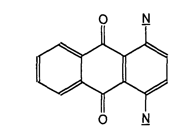
- a multifunctional linker molecule which is selected from the group including 1,4-dimercaptoacetamidobenzene derivatives of the general formula in which R 1,2 is independently selected from CH 3 and/or Cl, 1,4-dimercaptoacetamidocyclohexane having the formula , 1,4-dimercaptoacetamido-9,10-anthraquinone, having the formula , 1,5-dimercaptoacetamido-9,10-anthraquinone, having the formula , 1,8-dimercaptoacetamidooctane, having the formula , 1,4-dithiocarbamatobenzene, having the formula and 1,4-dithiocarbamatocyclohexane, having the following formula
- the multifunctional linker molecule is characterised in that the electron density on aromatic ⁇ -systems - as it can be described through the Hammett correlation parameter - and/or the degree of conjugation of the linker molecule is altered.
- Another aspect of the invention is a 1-, 2-, or 3-dimensional assembly of nanostructured units comprising a multifunctional linker according to the invention wherein the conductivity of the assembly is determined by the structure of the multifunctional linker molecule.
- the assembly according to the invention is characterised in that the nanostructured units are selected from the group comprising nanoparticles, such as metal, semiconductor, or core/shell semiconductor nanoparticles, nanowires, nanotubes, nanobelts, and electrodes.
- nanoparticles such as metal, semiconductor, or core/shell semiconductor nanoparticles, nanowires, nanotubes, nanobelts, and electrodes.
- an assembly which is characterised in that the absorption of the plasmon band is located between 500 nm and 600 nm, the functional units are Au-nanoparticles, the size of said Au-nanoparticles is about 5 to about 20 nm, the resistivity of the assembly is of the order of 10 2 ⁇ cm for a film thickness of about 30 nm, and the resistivity increases with decreasing temperature.
- an assembly which is characterised in that the absorption maximum of the plasmon band is located between 600 nm and 700 nm, the functional units are Au-nanoparticles, the size of said Au-nanoparticles is about 5 to about 20 nm, the resistivity of the assembly is of the order of 10 -1 to 10 ⁇ cm for a film thickness of about 30 nm, and the resistivity increases with decreasing temperature.
- an assembly according to the invention which is characterised in that the absorption spectrum shows the absorption characteristics of bulk metal films, the functional units are Au-nanoparticles, the size of said Au-nanoparticles is about 5 to about 20 nm, the resistivity of the assembly is of the order of 10 -2 ⁇ cm for a film thickness of about 30 nm, and the resistivity decreases with decreasing temperature.
- the problem is solved by the use of an assembly according to the invention as interconnects between nanowires and nanostructured units in 1-, 2-and 3-terminal devices, self-assembled metal coatings and/or self-assembled electrodes.
- the inventors of the present application have surprisingly found that a new design of nanoparticle linker molecules allows the effective tuning of the charge transport in nanoparticle linker assemblies from the insulating to the conducting limit.
- the inventors of the present invention have provided a method for tuning the charge transport through such assemblies by altering specific parts of the multifunctional linker molecules which provides a molecular tool-box that allows tuning of the charge transport in such assemblies from the insulating to the conducting limit. To the inventor's knowledge, so far a concept of how to alter molecular properties in order to tune the charge transport has not been suggested.
- Tuning of the charge transport is in one embodiment achieved by altering the energy levels of the molecular orbitals and the bonds formed between the nanoparticle and linker molecule.
- Four different means for altering the multifunctional linker molecules for tuning the charge transport through these assemblies are considered in this invention:
- nanoparticle according to the scope of the invention is used generically. It includes all varieties of metal and semiconducting nanoparticles and "clusters". The sizes of the nanoparticles can vary between 0.8 nm and up to the order of a few 100 nm. Further, on the interconnecting, linker molecules can establish interconnects between at least two nanoparticles, between at least one nanoparticle and a nanowire, between at least two nanowires, nanotubes or nanobelts, as well as between at least one nanoparticle or one nanowire, nanotube or nanobelt and macroscopic electrodes.
- “assemblies” refers to one-, two-, and three-dimensional assemblies of the above mentioned systems in all possible combinations.
- nanoparticles can be interconnected into one-, two-, or 3-dimensional arrays of nanoparticles.
- the synthesis of various nanoparticles is described in the literature as well as in patents.
- the nanoparticles can be prepared exhibiting different sizes.
- the preparation methods as well as the capping molecule largely determine the size distribution of the nanoparticles.
- a requirement for the successful assembly of the nanoparticles into an array is that the linker molecule can readily displace the capping molecule.
- the capping molecule could be exchanged with a different kind of capping molecule in a ligand exchange reaction prior to the assembly process (Jahn, W. (1999) Journal of Structural Biology, 127, 106-112 "Review: Chemical aspects of the use of gold clusters in structural biology.”, Brown, L.O., Hutchinson, J.E. (1997) J. Am. Chem. Soc., 119, 12834-12835 "Convenient preparation of stable, narrow-dispersity, gold nanocrystals by ligand exchange reactions.”, Aguila, A. Murray, R.W. (2000), Langmuir, 16, 5949-5954 "Monolayer-protected clusters with fluorescent dansyl ligands.”).
- the synthesis of the multifunctional, i.e. bi-, and polyfunctional linker molecules is based on substitution reactions that are described in the literature. Two possible synthetic routes are considered.
- route 1 the amino substituents of the starting materials are converted into bromoacetamido groups via a nucleophilic substitution reaction with bromoacetylbromide.
- the bromoacetamido group is converted into a thioacetate ester by reaction with potassium thioacetate.
- the thioacetate ester is converted into a thiol via a cleavage reaction as it is described by Yelm (Yelm, K.E. (1999), Tetrahedron Letters 40, 1101-1102.
- the first layer of nanoparticles can be deposited onto a substrate by means of self-assembling bi-functional organic monolayers as bridge compounds.
- the first layer of nanoparticles can self-assemble on the functional substrate and be subsequently interconnected by the linker molecules.
- the linker molecules displace the capping molecules from the surface of the nanoparticles leaving a free linker group, e.g. a thiol group at the top of the nanoparticle film for the assembly of the next nanoparticle layer.
- This assembly process is also referred to as the layer-by-layer assembly technique (Brust, M., Bethell, D., Kiely, C.J., Schiffrin, D.J., (1998) Langmuir, 14, 5425-5429 "Self-assembled gold nanoparticle thin films with nonmetallic optical and electronic properties.”).
- a one-step formation of 3-dimensional nanoparticles can be achieved via the preparation of a co-solution of nanoparticles and linker molecules and exposing this to a functionalised substrate (Whetten, R.L., Khoury, J.T., Alvarez, M.M., Murthy, S., Vezmar, I., Wang, Z.L., Stephens, P.W., Cleveland, C.C., Luedtke, W.D., Landmann, U. (1996) Adv. Mater., 8, 428).
- a functionalised substrate Wang, Z.L., Stephens, P.W., Cleveland, C.C., Luedtke, W.D., Landmann, U. (1996) Adv. Mater., 8, 428).
- a close packed monolayer of nanoparticles can also be produced using the Langmuir-Blodgett or the Langmuir-Schaeffer technique (Musick, M.D., Keating, C.D., Keefe, N.H., Natan, M.J . (1997) Chem. Mater., 9, 1499-1501 "Stepwise construction of conductive Au colloid multilayers from solution.”, Markkovich; G., Leff, D.V., Chung, S .Q., S hinder, H.M. Dunn, B., Heath, J.R.
- the assembly process can be monitored using absorption spectroscopy.
- the optical density of the plasmon band provides information about the thickness of the self-assembled film.
- the absorption spectrum contains also information about the character of the nanoparticle film, since the optical properties of the particles are determined by the contributions from the individual particles and the collective properties of the ensemble.
- the plasmon band is attributed to the collective oscillations of the free conduction electrons and their response to an incident electromagnetic field. It can be considered as a hybrid resonance from the cooperative behaviour of the d-band and conduction electrons.
- Chem., 103, 3529-3533 "Alloy formation of gold-silver nanoparticles and the dependence of the plasmon absorption on their composition.”, Alvarez, M.M., Khoury, J.T., Schaaff, T.G., Shafigulli, M.N., Vezmar, I., Whetten, R.L. (1997) J . Phys. Chem., 101, 3706-3712 "Optical absorption spectra of nano-crystal gold molecules.”).
- the plasmon frequency is the dependence on the electron density and on the effective mass or optical mass of the electron, which includes the coupling of the free electrons to the ion core (Kreibig, U., Genzel, L. (1985) Surface Science, 156, 678-700 "Optical absorption of small metallic particles.”).
- the plasmon frequency is the dependence on the electron density and on the effective mass or optical mass of the electron, which includes the coupling of the free electrons to the ion core (Kreibig, U., Genzel, L. (1985) Surface Science, 156, 678-700 "Optical absorption of small metallic particles.”).
- the band-gap absorption can be used for monitoring the assembly process.
- the electrical properties of such one-, two-, or, three- dimensional arrays of nanoparticles are determined by material composition and size of the nanoparticles used, the stabilising organic ligand, and by the properties of the linker molecules.
- tunnel junctions exhibiting an electrical capacitance of less than 10 -18 F are created (Single charge tunnelling - Coulomb blockade phenomena in solids; Eds. Devoret, M.H., Grabert, H. (1992) Nato ASI Series, Vol.. 294, Plenum, New York).
- the insulating molecular layer around the nanoparticle that serves as an insulating barrier facilitates electron tunnelling or hopping.
- the charge transport in these structures can be tuned from the metallic to the insulating limit by varying the size of the particles and the strength of the coupling between them.
- the electron transport properties of these thin films depend on the properties of the insulating layer and the linker molecules (Brust, M., Bethell, D., Kiely, C.J., Schiffrin, D.J., (1998) Langmuir, 14, 5425-5429 "Self-assembled gold nanoparticle thin films with nonmetallic optical and electronic properties.”, Neugebauer, C.A., Webb, M.B. (1962) Journal of Applied Physics, 33, 74-82 "Electrical conduction mechanism in ultrathin, evaporated metal films.”).
- Figure 1 Schematic drawing of the synthetic routes for substituting amino functionalised molecules with dimercaptoacetamido groups (a) or with thiocarbamates (b).
- Figure 2 Schematic drawing of the linker molecules synthesised according to the routes described in Figures 1a and b.
- 1,4-dimercaptoacetamidobenzene 1
- 1,4-dimercaptoacetamido-2,5-dimethylbenzene 2
- 1,4-dimercaptoacetamido-2,5-dichlorobenzene 3
- 1,4-dimercaptoacetamidocyclohexane 4
- 1,4-dimercaptoacetamido-9,10-anthraquinone 5
- 1,8-dimercaptoacetamido-9,10-anthraquinone 6
- 1,4-dithiocarbamatobenzene 7
- 1,4-dithiocarbamatocyclohexane 8
- 1,8-dimercaptoacetamidoctane 9
- the commercially available nonanedithiol 10
- Figure 3 I-V characteristics of Au-nanoparticles interconnected by the linker molecules 1 (-), 2 (---), 3 ( ⁇ ), 4 ( ⁇ - ⁇ - ⁇ ), and 10 (---) and self-assembled onto interdigiated Au electrode structures by the layer-by-layer assembly technique to a film thickness of approx. 30 nm.
- Figure 4 Temperature dependence of the conductivity of Au-nanoparticles interconnected by the linker molecules 1 (-) and 7 (- - -) and self assembled onto interdigitated Au-electrode structures by the layer-by-layer assembly technique to a film thickness of approx. 30 nm.
- Figure 5 I-V characteristics of Au-nanoparticles interconnected by the linker molecules 5 (-), 6 (---), 7 ( ⁇ ), 8 ( ⁇ - ⁇ - ⁇ ), and 9 (---) and self-assembled onto interdigiated Au electrode structures by the layer-by-layer assembly technique to a film thickness of approx. 30 nm.
- Figure 6 Absorption spectra of Au-nanoparticles interconnected by linker molecules 1 (-), 6 (- - -), and 7 ( ⁇ ) assembled onto a silanized glass substrate by the layer-by-layer assembly technique to a film thickness of approx. 30 nm.
- the electrodes Prior to the assembly process, the electrodes were functionalised with a (3-aminopropyl)-dimethylethoxysilane.
- a 1 mM solution of the linker molecule was used and the concentration of the Au-nanoparticle solution was approx. 0.5 mM.
- the assembly process was monitored using UV/VIS absorption spectroscopy.
- the film thickness for all assemblies was adjusted to an optical density (O.D.) of approximately 0.32-0.35 at the maximum of the plasmon band, which amounts to a film thickness of roughly 30 nm as determined by AFM. The thickness of the films varies slightly from assembly to assembly.
Abstract
Description
- The invention relates to tuned multifunctional linker molecules for charge transport through organic-inorganic composite structures and assemblies and devices comprising such multifunctional linker molecules. The invention further relates to the use of such tuned multifunctional linker molecules.
- 1-, 2-, and 3-dimensional assemblies of nanometer-sized particles coupled by multifunctional linker molecules have potential applications in nanometer-sized computational or memory devices. A key enabling technology for designing such nanoelectronic devices is the ability to tune the conductivity in such assemblies by altering the structure of the linker molecules.
- The multifunctional linker molecules connect the nanoparticles with each other through tunnel barriers. It has been shown in the literature that charge transport via through-bond tunneling is a major channel for charge transport (Slowinskli, K., Chamberlain, R.V., Miller, C.J., Majda, M. (1997) J.Am. Chem. Soc., 119, 11910-11919 "Through-bond and chain-to-chain coupling. Two pathway electron tunneling through liquid alkanethiol monolayers on mercury electrodes.").
- Further it has been suggested that the orbital overlap between the nanoparticle and the binding group of the linker molecule is an important factor in charge transport through these assemblies (Bakkers, E.P.A.M., Marsmann, A.W., Jenneskens, L.M., Vanmaekelbergh, D. (2000) Angewandte Chemie, 112, 2385-2388 "Abstandsabhängiger Elektronentransfer in Au/Spacer/Q-CdSe-Anordnungen."). The electrical properties of various 1-dimensional, 2-dimensional, and 3-dimensional assemblies of nanoparticles have been described in the literature. In 2-dimensional superlattice arrays of Au-nanoparticles molecularly linked by aryl di-isonitriles, both nonlinear Coulomb-charging behavior as well as Ohmic behavior has been reported in the literature (Janes, D .B., Kolaguta, V.R., Osifchin, R.G., Bielefeld, J.D., Andres, R.P., Henderson, J.I., Kubiak, C.P. (1995) Superlattices and Microstructures, 18, 275-282 "Electronic conduction through 2D arrays of nanometer diameter metal clusters.", Andres, R.P., Bielefeld, J.D., Henderson, J.I., Janes, D.B., Kolagunta, V.R., Kubiak, C.P., Mahoney, W.J., Osifchin, R.G. (1996) Science, 273, 1690-1693, "Self-assembly of a two-dimensional superlattice of molecularly linked metal clusters.", Chen, E., Ahmed, H., Nakazoto, K. (1995) Applied Physics Letters. 66, 3383-3384 "Coulomb blockade at 77K in nanoscale metallic islands in a lateral nanostructure."). Ohmic charge transport has been observed in 3-dimensional arrays of Au and Ag nanoparticles. The resistance in such films can vary between R > 107 Ω to R < 102 Ω, analogous to what has been observed in percolated films of metal grains depending on the grain size and the dot to dot distances (Musick, M.D., Keating, C.D., Keefe, N.H., Natan, M.J . (1997) Chem. Mater., 9, 1499-1501 "Stepwise construction of conductive Au colloid multilayers from solution.", Neugebauer, C.A., Webb, M.B. (1962) Journal of Applied Physics, 33, 74-82 "Electrical conduction mechanism in ultrathin, evaporated metal films.").
- WO 96/07487 describes the synthesis of nanoparticle materials exhibiting controlled electronic, magnetic and/or optical properties. Such synthesized materials can then be incorporated into electronic, magnetic and/or optical devices, such as, for example, resistors, diodes, transistors, switches, displays, lasers, photovoltaic and magnetic devices. Further, the application describes the production of thin film structures that can be used for said devices.
- In addition, a 1-step formation of 3-dimensional nanoparticles is described via the preparation of a co-solution of nanoparticles and linker molecules and exposing this to a functionalized substrate. WO 96/07487 also describes a layer-by-layer assembly technique for producing thin film structures from particles of nanometer dimensions and polyfunctional linker molecules comprising a hydrocarbon skeleton with at least two functional groups (which may be the same or different) capable of binding to other particles or substrates.
- WO96/07487 further proposes a prototype of a nanostructured array of quantum dots with adjustable electronic conductivity in the range typical for semi-conductors. The properties of the material can be tuned by building moieties into the linker molecules that can act as electron donors or acceptors. Further, the resistivity of the material changes dramatically as a function of the chain length of the linker molecule.
- WO96/07487 in general suggests activated electron hopping as the principle mechanism for charge transport.
- Nevertheless, despite the above-mentioned progress, there is still the need in the art to improve multifunctional linker molecules in order to allow the tuning and/or fine tuning of the conductivity of nanostructure assemblies from the insulating to the conducting limit.
- Accordingly, the problem underlying the present invention is to provide improved multifunctional linker molecules for tuning the conductivity in nanoparticle-linker assemblies which may be used, e.g., in the formation of electronic networks and circuits and thin films of nanoparticles allowing a high density arrangement.
- The problem is solved according to the invention by providing a multifunctional linker molecule of the general structure
X is the central body of the molecule,
FUNC1 and FUNC2 independently of each other are molecular groups introducing a dipole moment and/or capable of forming intermolecular and/or intramolecular hydrogen bonding networks, with the provisio that they are not of hydrocarbon nature, and
CON 1 and CON 2 independently of each other are molecular groups binding to nanostructured units comprising metal, alloys of metals, metal core/shell materials, semiconductor or semiconductor core shell materials. - The multifunctional linker molecule according to the invention has several advantages over the linker molecules described in WO 96/07487. First, the general structures are different in that the general structure of the linker of WO 96/07487 can schematically be seen as [Connecting group] [Hydrocarbon skeleton] [Connecting group] in which the connecting group is capable of binding to nanoparticles.
- In contrast, the general structure of the multifunctional linker molecule according to the invention can be represented as [Connecting group 1][Functional group 1][Central body][Functional group 2] [Connecting group 2] in which functional groups are introduced between the central body and the connecting groups which are capable of binding to nanoparticles. The functional groups introduce different specific functions into the inventive linker molecule and are not of hydrocarbon nature. Therefore, the molecular structure of the multifunctional linker molecule is different from WO 96/07487, which results in a drastic improvement of the cpability for tuning the charge transport through organic/inoganic composite structures according to the invention.
- The functional groups add the aspects of introducing a dipole moment into the structure and forming intermolecular and/or intramolecular hydrogen bonding networks. These features can support the ordering of the organic/inorganic composite structures and allows the tuning of the charge transport.
- Thus, the design of the linker molecules according to the invention provides a means of tuning the conductivity through these assemblies. To the inventors knowledge, so far a concept of how to alter molecular properties in order to tune the charge transport has not been suggested. This invention concerns a strategy for tuning the conductivity through such assemblies by altering specific parts of multifunctional linker molecules providing a molecular tool-box that allows tuning of the conductivity in such assemblies from the insulating to the conducting limit. This is again in contrast to WO 96/07487, which allows tuning of the conductivity only in the semiconducting range.
- Preferred is a multifunctional linker molecule according to the invention, in which CON1 and CON2 are identical or different and FUNC1 and FUNC2 are identical or different.
- In one embodiment, the multifunctional linker molecule according to the invention is characterized in that it exhibits a length between about 8 Å and about 30 Å.
- Preferred is a multifunctional linker molecule according to the invention in which X is a structure having a hydrocarbon skeleton with two identical or different substituents that are used for connecting to and/or forming of the molecular groups FUNC1 and FUNC2.
- The central part of the linker molecule can also consist of alkanes, alkenes, alkynes, and combinations thereof which exhibit two end groups comprising amines, carboxylic acids, sulfonic acids and phosphonic acids.
- Further preferred is a multifunctional linker molecule according to the invention, which is characterized in that the substituents of X are selected from the group comprising amines, carboxylic acids, sulfonic acids and phosphonic acids. Even more preferred is, that the substituents of X are directed at an angle α relative to one another such that 90° < α < 270°.
- In yet another embodiment of a multifunctional linker molecule according to the invention, X comprises a conjugated system, an aromatic π-system and/or contains heteroatoms, like N, O or S, and/or contains at least one electron donating substituent, like CH3, O-, COO- N(CH3)2 or NH2 and/or electron accepting substituent, like CN, COCH3, CONH2, CO2CH3, N(CH3)3 +, NO2, F, Cl, Br, I, OCF3, or SO2NH2.
- Most preferred is a multifunctional linker molecule according to the invention, which is characterized in that X is selected from the group comprising a) linear or branched structures of alkanes, alkenes, alkynes and combinations thereof comprising 3-12 carbon atoms and exhibiting two end substituents as mentioned above;
-

 and derivatives thereof containing heteroatoms, like N, S, and/or O, or electron donating or accepting substituents; R can be methyl, phenyl or alkoxyl and wherein FUNC1 and FUNC2 are attached via the N-atoms of the two amine substituents indicated by N; structures having the general formula


 and derivatives thereof containing electron donating or accepting substituents wherein FUNC1 and FUNC2 are attached via the N-atoms of the amine substituents indicated by N; structures having the general formula


 and derivatives thereof containing heteroatoms, like N, S, and/or O, or electron donating or accepting substituents; and wherein FUNC1 and FUNC2 are attached via the carbon atoms of the two carboxylic acid substituents indicated by C; structures having the general formula

 wherein FUNC1 and FUNC2 are attached via the carbon atoms of the two carboxylic acid substituents indicated by C; structures having the general formula
 and derivatives thereof containing electron donating or accepting substituents wherein FUNC1 and FUNC2 are attached via the N- or S-atoms of the two amine or sulfonic acid substituents indicated by N and S; structures having the general formula


 in which Z represents amine (Z = N) or a carboxymethyl (Z = CH(R)C) residue, wherein R is an amino acid side chain and FUNC1 and FUNC2 are attached via Z; and c) electron donors like hydroquinones and electron acceptors, like quinones and diimides carrying two substituents as mentioned above.
- In a still further embodiment according to the invention, the multifunctional linker molecule is characterized in that FUNC1 and FUNC2 independently of each other are connected to X via N, C, S, or P, and are selected from the group including
-NH, -NHCO, -NHCONH, -NHCSNH, -NHCONHNH, -NHCSNHNH, -NHCONHNHCO, and -NHCONHNHCO in case of a connection via N;
-CONH, -CONHNH, and -CONHNHCO in case of a connection via C;
-SO2 NH, -SO2NHNH, and -SO2NHNHCO in case of a connection via S; and
-PO2 NH, -PO2NHNH, and -PO2NHNHCO in case of a connection via P. - In an even more preferred embodiment of a multifunctional linker molecule according to the invention, CON1 and CON2, connected to FUNC1 and FUNC2 via NH or CO, independently of each other are selected from the groups including
-(CHR)nCOOH; -(CHR)nNC; -(CHR)nNH2; -(CHR)nNHCS2H; -(CHR)nOPO3H2; - (CHR)nOSO3H; -(CHR)nPO3H2; -(CHR)nSH; -(CHR)nSO3H; -CSOH; and -CS2H in case of a connection via NH; and
-(CHR)nCOOH; -(CHR)nNC; -(CHR)nNH2; -(CHR)nNHCS2H; -(CHR)nOPO3H2;-(CHR)nOSO3H; -(CHR)nPO3H2; -(CHR)nSH; and -(CHR)nSO3H in case of a connection via CO;
where R is H, CH2OH, or CH3 and n is 1 or 2, and ionic forms thereof. - One example of how the different units can be put together can schematically be described as follows:

- In a further embodiment of the inventive multifunctional linker molecule, the thiocarbamates formed from secondary amines are directly attached to the central body X.
- Other preferred embodiments of the inventive multifunctional linker molecule are characterized in that CON1 and CON 2 independently of each other comprise branched molecular structures.
- Most preferred is a multifunctional linker molecule which is selected from the group including 1,4-dimercaptoacetamidobenzene derivatives of the general formulain which R1,2 is independently selected from CH3 and/or Cl,

1,4-dimercaptoacetamidocyclohexane having the formula, 1,4-dimercaptoacetamido-9,10-anthraquinone, having the formula , 1,5-dimercaptoacetamido-9,10-anthraquinone, having the formula
 , 1,8-dimercaptoacetamidooctane, having the formula
 , 1,4-dithiocarbamatobenzene, having the formula
 and 1,4-dithiocarbamatocyclohexane, having the following formula

- Other preferred embodiments of the multifunctional linker molecule according to the invention are selected from the group of the following formulae:


- In an even more preferred embodiment of the invention, the multifunctional linker molecule is characterised in that the electron density on aromatic π-systems - as it can be described through the Hammett correlation parameter - and/or the degree of conjugation of the linker molecule is altered.
- Another aspect of the invention is a 1-, 2-, or 3-dimensional assembly of nanostructured units comprising a multifunctional linker according to the invention wherein the conductivity of the assembly is determined by the structure of the multifunctional linker molecule.
- Preferably, the assembly according to the invention is characterised in that the nanostructured units are selected from the group comprising nanoparticles, such as metal, semiconductor, or core/shell semiconductor nanoparticles, nanowires, nanotubes, nanobelts, and electrodes.
- The problem of the invention is further solved by an assembly, which is characterised in that the absorption of the plasmon band is located between 500 nm and 600 nm, the functional units are Au-nanoparticles, the size of said Au-nanoparticles is about 5 to about 20 nm, the resistivity of the assembly is of the order of 102 Ω cm for a film thickness of about 30 nm, and the resistivity increases with decreasing temperature.
- More preferred is an assembly which is characterised in that the absorption maximum of the plasmon band is located between 600 nm and 700 nm, the functional units are Au-nanoparticles, the size of said Au-nanoparticles is about 5 to about 20 nm, the resistivity of the assembly is of the order of 10-1 to 10 Ω cm for a film thickness of about 30 nm, and the resistivity increases with decreasing temperature.
- Most preferred is an assembly according to the invention which is characterised in that the absorption spectrum shows the absorption characteristics of bulk metal films, the functional units are Au-nanoparticles, the size of said Au-nanoparticles is about 5 to about 20 nm, the resistivity of the assembly is of the order of 10-2 Ω cm for a film thickness of about 30 nm, and the resistivity decreases with decreasing temperature.
- In a still further aspect of the invention, the problem is solved by the use of an assembly according to the invention as interconnects between nanowires and nanostructured units in 1-, 2-and 3-terminal devices, self-assembled metal coatings and/or self-assembled electrodes.
- The inventors of the present application have surprisingly found that a new design of nanoparticle linker molecules allows the effective tuning of the charge transport in nanoparticle linker assemblies from the insulating to the conducting limit.
- The inventors of the present invention have provided a method for tuning the charge transport through such assemblies by altering specific parts of the multifunctional linker molecules which provides a molecular tool-box that allows tuning of the charge transport in such assemblies from the insulating to the conducting limit. To the inventor's knowledge, so far a concept of how to alter molecular properties in order to tune the charge transport has not been suggested.
- Tuning of the charge transport is in one embodiment achieved by altering the energy levels of the molecular orbitals and the bonds formed between the nanoparticle and linker molecule. Four different means for altering the multifunctional linker molecules for tuning the charge transport through these assemblies are considered in this invention:
- 1) Altering of the electron density on aromatic π-systems through different substituents as it
can be described through the Hammett correlation parameter σp +.
It is important for the design of nanostructured electronic devices to have means for fine tuning
the HOMO-LUMO levels of the linker molecules, in order to adjust the HOMO and
LUMO levels of the linker molecules with respect to the Fermi energy level of metal particles
as well as the energy band levels of semiconducting particles. In this invention, we provide a
new approach for providing a series of linker molecules exhibiting an aromatic π-system
where the electron density on the aromatic π-system of the multifunctional linker molecule is
varied in a defined manner as it can be described by the so-called Hammett correlation parameter
σp +. This parameter describes the electron donating and accepting properties of substituents
on aromatic π-systems, which alter the energy gap between the HOMO and LUMO
energy levels in the linker molecules, and hence provides a means for fine-tuning the charge
conduction through the assemblies.2) Altering the degree of charge transport through linker molecules exhibiting conjugated π-systems:
- a) Altering the particle-particle interaction by changing the degree of conjugation in the linker molecule through cross-conjugation an/or by introducing non-conjugated molecular structures into the linker molecule.
- b) Introducing electron-accepting groups onto conjugated π-systems of the linker molecule, facilitating the electron transport across the linker molecule. The possibilities for influencing charge transport by changing the degree of delocalisation in conjugated π-systems via cross-conjugation has been suggested for molecular wires. Theoretical calculations have shown that in case of molecular wires made out of coupled porphyrin systems, cross conjugation leads to a pronounced attenuation of the coupling interaction between HOMO-orbitals (Hush, N.S., Reimers, J.R., Hall, L.E., Johnston, L.A., Crossley, M.J. (1998) Annals of the New York Academy of Sciences, 852, 1-21 (Edts. Aviram, A., Ratner, M.) "Optimization and chemical control of porphyrin-based molecular wires and switches."). Cross-conjugation interrupts the long-range electronic coupling of conjugated π-bonds and hence it is a possibility to fine-tune the conductivity of linker molecules exhibiting conjugated π-systems.Besides the possibility of influencing the charge transport in conjugated linker molecules via cross-conjugation the charge transport can also be altered by introducing electron accepting groups into the linker molecules. Quinones are very efficient electron acceptors that are implemented into the light harvesting systems of plants. It has been suggested that they have been developed by the plants in order to facilitate electron transport in the photosynthetic system. Similarly it can be envisioned that efficient electron acceptors such as anthraquinones (Karuktis, K.K., Gruber, S.M., Fruetel, J.A., Boegeman, S.C. (1988) Biochim. Biophys. Acta, 932, 84-90 "Quenching of chlorophyll fluorescence by substituted anthraquinones.") for example can facilitate the electron transport in such multidimensional assemblies.
- 3) Influencing the charge transport properties through the contacting molecular groups
CON1,2.
The molecular groups forming the connection between the different nanostructured units, e.g.
wires, active elements, and possibly electrodes have a central function in the charge transport,
since the molecular design of this group is defining the type of bond that is formed the linker
molecule and the different nanostructured units. Included is also, that the electrode or wire
metal can be altered to alter the atom from the nanostructured unit that participates in forming
the contact to the linker molecule depending on what type of tunnel barrier should be established
for a specific interconnect.The role of the contacts has been studied theoretically by implementing the contacts to Au-particles
into the extended calculations of the HOMO and LUMO levels of a 1,4 benzene dithiolate
(Emberly, E.G., Kirczenow, G. (1998) Annals of the New York Academy of Sciences,
852, 1-21 (Edts. Aviram, A., Ratner, M.) "Theory of electrical conductance through a
molecule."). These calculations show that, in a model system consisting of two Au-particles
connected by one benzene dithiolate, conduction can occur via two pathways:
- a) Through the states derived from the benzene dithiolate HOMO and LUMO levels.
- b) Through the energy levels arising from hybrid Au particle-benzene dithiolate states. However, the linker molecule/particle interface has a very low density of states. Experiments by Reed et al. suggest that the contacts are atomically terminated, i.e. the S-atoms are attached to single Au-atoms (Reed, M.A., Zhou, C., Mueller, C.J., Burgin, T.P., Tour, J.M. (1997) Science, 278, 252). It has been shown for Au-S systems, that the Au atom cocontributes states at the Fermi level, while the S atom contributes p states, thereby forming σ bonds (Di Ventra, Pantelidis, S.T., Lang, B.D. (2000) Phys. Rev. Lett., 84, 979-982 "First - principles calculation of transport properties of a molecular wire.", Johansson, A., Stafström, S. (2000) Chem. Phys. Lett., 322, 301-306 "Interactions between molecular wires and a gold surface."). Thus the linker molecule/particle interface forms a tunnel barrier for the charge transport. Therefore, binding of the linker molecule via single or multiple binding groups, e.g. thiols or thiocarbamates, should have a strong influence on the properties of the tunnel barrier and hence on the charge transport through these assemblies.Further, theoretical calculations have shown that replacement of Au atoms by A1 atoms should reduce the tunnel barrier. A1 atoms can contribute to the interconnect p-orbitals and thus are capable to form π-orbitals with S atoms of linker molecules (Di Ventra, Pantelidis, S.T., Lang, B.D. (2000) Phys. Rev. Lett., 84, 979-982 "First - principles calculation of transport properties of a molecular wire.").
- 4) Influencing the charge transport by altering the functional groups of the linker molecule
that is located at the nanoparticle/linker molecule interface:
- Increasing the electron coupling through two interconnected circuit elements by introducing a hydrogen-bonding network into the linker molecules.
-
- It has been shown that a hydrogen bond network linking amide bonds in alkane monolayers leads to an increase in the electronic coupling between an electrode and a ferrocene molecule (Sek, S., Misicha, A., Bileicz, R. (2000) J. Phys. Chem. B, 104, 5399-5402 "Effect of inter-chain hydrogen bonding on electron transfer through alkanethiol monolayers containing amide bonds."). The same effect has also been observed for the electron tunneling between mercury-mercury tunnel junctions across alkane-thiolate bilayers (Slowinski, K. Fong, H.K., Mayda, M. (1999) J. Am. Chem. Soc., 121, 7257-7261 "Mercury-Mercury tunneling junctions. 1. Electron transfer across symmetric and asymmetric alkane thiolate bilayers.").
- It is to be understood that the term "nanoparticle" according to the scope of the invention is used generically. It includes all varieties of metal and semiconducting nanoparticles and "clusters". The sizes of the nanoparticles can vary between 0.8 nm and up to the order of a few 100 nm. Further, on the interconnecting, linker molecules can establish interconnects between at least two nanoparticles, between at least one nanoparticle and a nanowire, between at least two nanowires, nanotubes or nanobelts, as well as between at least one nanoparticle or one nanowire, nanotube or nanobelt and macroscopic electrodes. Thus, "assemblies" refers to one-, two-, and three-dimensional assemblies of the above mentioned systems in all possible combinations.
- Various types of metal or semi-conducting nanoparticles can be interconnected into one-, two-, or 3-dimensional arrays of nanoparticles. The synthesis of various nanoparticles is described in the literature as well as in patents. Depending on the preparation method and the capping molecule used, the nanoparticles can be prepared exhibiting different sizes. The preparation methods as well as the capping molecule largely determine the size distribution of the nanoparticles. A requirement for the successful assembly of the nanoparticles into an array is that the linker molecule can readily displace the capping molecule. In case a particular capping molecule can not be displaced by the linker molecules, the capping molecule could be exchanged with a different kind of capping molecule in a ligand exchange reaction prior to the assembly process (Jahn, W. (1999) Journal of Structural Biology, 127, 106-112 "Review: Chemical aspects of the use of gold clusters in structural biology.", Brown, L.O., Hutchinson, J.E. (1997) J. Am. Chem. Soc., 119, 12834-12835 "Convenient preparation of stable, narrow-dispersity, gold nanocrystals by ligand exchange reactions.", Aguila, A. Murray, R.W. (2000), Langmuir, 16, 5949-5954 "Monolayer-protected clusters with fluorescent dansyl ligands.").
- The synthesis of the multifunctional, i.e. bi-, and polyfunctional linker molecules is based on substitution reactions that are described in the literature. Two possible synthetic routes are considered. In
route 1, the amino substituents of the starting materials are converted into bromoacetamido groups via a nucleophilic substitution reaction with bromoacetylbromide. In the second step, the bromoacetamido group is converted into a thioacetate ester by reaction with potassium thioacetate. The thioacetate ester is converted into a thiol via a cleavage reaction as it is described by Yelm (Yelm, K.E. (1999), Tetrahedron Letters 40, 1101-1102. "A simple method for in situ generation of thiols from thioacetates.") as well as Wallace and Springer (Wallace, O.B., Springer, D.M. (1998) Tetrahedron Letters, 39, 2963-2964. "Mild, selective deprotection of thioacetates using sodium thiomethoxide."). Alternatively, the reaction can be carried out as described by Martin (Martin, T.A.; Comer, W.T.; J. Med. Chem. (1985), 28, 910-914 "N-[[(Mercaptoacetyl)amino]benzoyl]glycines as mucolytic agents") in an aqueous methanolic NaOH solution. A one step reaction pathway for preparing different chelates from bis(mercaptoacetamide)-p-phenylenediamine has been described by Aswar, A.S. and Bhadange, S.G. (J. Indian Chem. Soc. (1997) 74, 679-682). The reaction is shown in Figure 1a (prior art). Inroute 2, the amino substituents are directly reacted with carbon disulfide and base to give thiocarbamate salts. This reaction is described in references (McCubbin, Q.J., Stoddart, F.J., Welton, T., White, A.J.PL., Williams, D.J. (1998), Innorganic Chemistry 37, 3753-3758. "Dithiocarbamate-functionalised dendrimers as ligands for metal complexes.", Almirall, E ., Fragoso, A., Cao, R. (1999)Electrochemistry Communications 1, 10-13. "Molecular recognition of a self-assembled monolayer of a polydithiocarbamate dervative of β-cyclodextrin on silver.", Matsumoto, I., Nakagawa, K., Matsuzaki, M., Horiuchi, K. (1975), US 3,875,170 "Pyridine-bis-(dithio)-carbamate derivatives.") and depicted in Figure 1b (prior art). - Different means for the assembly of the thin films have been described in the literature and in patents. The first layer of nanoparticles can be deposited onto a substrate by means of self-assembling bi-functional organic monolayers as bridge compounds. The first layer of nanoparticles can self-assemble on the functional substrate and be subsequently interconnected by the linker molecules. The linker molecules displace the capping molecules from the surface of the nanoparticles leaving a free linker group, e.g. a thiol group at the top of the nanoparticle film for the assembly of the next nanoparticle layer. This assembly process is also referred to as the layer-by-layer assembly technique (Brust, M., Bethell, D., Kiely, C.J., Schiffrin, D.J., (1998) Langmuir, 14, 5425-5429 "Self-assembled gold nanoparticle thin films with nonmetallic optical and electronic properties."). Alternatively, a one-step formation of 3-dimensional nanoparticles can be achieved via the preparation of a co-solution of nanoparticles and linker molecules and exposing this to a functionalised substrate (Whetten, R.L., Khoury, J.T., Alvarez, M.M., Murthy, S., Vezmar, I., Wang, Z.L., Stephens, P.W., Cleveland, C.C., Luedtke, W.D., Landmann, U. (1996) Adv. Mater., 8, 428). A close packed monolayer of nanoparticles can also be produced using the Langmuir-Blodgett or the Langmuir-Schaeffer technique (Musick, M.D., Keating, C.D., Keefe, N.H., Natan, M.J . (1997) Chem. Mater., 9, 1499-1501 "Stepwise construction of conductive Au colloid multilayers from solution.", Markkovich; G., Leff, D.V., Chung, S .Q., Soyez, H.M. Dunn, B., Heath, J.R. (1997) Applied Physics Letters, 70, 3107-3109 "Parallel fabrication and single-electron charging of devices based on ordered, two-dimensional phases of organically functionalized metal nanocrystals.") These techniques allow the transfer of a well-defined monolayer to a substrate, the packing density of which can be determined through the compression of the nanoparticle film at the air-water interface. Instead of using multifunctional organic molecules as bridge compounds it is also possible to deposit e.g. charged nanoparticles onto a substrate utilizing electrostatic interactions (Sato, T., Haskko, D., Ahmed, H., (1996) EP0788149A1 "Method of depositing nanometre scale particle.", Ahmed, H., Sato, T. (1998) EP0865078 "Method for depositing nanometer scale particles.").
- For certain metal particles, the assembly process can be monitored using absorption spectroscopy. The optical density of the plasmon band provides information about the thickness of the self-assembled film. Furthermore, depending on the material and composition of the nanoparticles the absorption spectrum contains also information about the character of the nanoparticle film, since the optical properties of the particles are determined by the contributions from the individual particles and the collective properties of the ensemble. The plasmon band is attributed to the collective oscillations of the free conduction electrons and their response to an incident electromagnetic field. It can be considered as a hybrid resonance from the cooperative behaviour of the d-band and conduction electrons. A simple description of the plasmon frequency combining the resonance condition and the dielectric constant for a free electron gas is:
ne eff - For semiconducting nanoparticles, the band-gap absorption can be used for monitoring the assembly process.
- The electrical properties of such one-, two-, or, three- dimensional arrays of nanoparticles are determined by material composition and size of the nanoparticles used, the stabilising organic ligand, and by the properties of the linker molecules. Arranging small particles into an array exhibiting small spatial distance, tunnel junctions exhibiting an electrical capacitance of less than 10-18 F are created (Single charge tunnelling - Coulomb blockade phenomena in solids; Eds. Devoret, M.H., Grabert, H. (1992) Nato ASI Series, Vol.. 294, Plenum, New York). The insulating molecular layer around the nanoparticle that serves as an insulating barrier facilitates electron tunnelling or hopping. The charge transport in these structures can be tuned from the metallic to the insulating limit by varying the size of the particles and the strength of the coupling between them.
- The electron transport properties of these thin films depend on the properties of the insulating layer and the linker molecules (Brust, M., Bethell, D., Kiely, C.J., Schiffrin, D.J., (1998) Langmuir, 14, 5425-5429 "Self-assembled gold nanoparticle thin films with nonmetallic optical and electronic properties.", Neugebauer, C.A., Webb, M.B. (1962) Journal of Applied Physics, 33, 74-82 "Electrical conduction mechanism in ultrathin, evaporated metal films."). Activation energies in the range between 30 - 100 meV depending on the electronic structure of the linker molecule, the dot to dot distance and the size of the nanoparticles, have been reported for such assemblies (Brust, M ., Bethell, D., Schiffrin, D.J., Kiely, C.J. (1995) Advanced Materials, 7, 795-797. "Novel gold-ditiol nano-networks with non-metallic electronic properties.", Janes, D, Kolaguta, LV.R., Osifchin, R.G., Bielefeld, J.D., Andres, R.P., Henderson, J.I., Kubiak, C.P. (1995) Superlattices and Microstructures, 18, 275-282 "Electronic conduction through 2D arrays of nanometer diameter metal clusters.", Brust, M., Bethell, D., Kiely, C.J., Schiffrin, D.J., (1998) Langmuir, 14, 5425-5429 "Self-assembled gold nanoparticle thin films with nonmetallic optical and electronic properties.").
- The invention is now further illustrated by the accompanying figures and examples from which further embodiments, features and examples may be taken.
- Figure 1: Schematic drawing of the synthetic routes for substituting amino functionalised molecules with dimercaptoacetamido groups (a) or with thiocarbamates (b).
- Figure 2: Schematic drawing of the linker molecules synthesised according to the routes described in Figures 1a and b. 1,4-dimercaptoacetamidobenzene (1), 1,4-dimercaptoacetamido-2,5-dimethylbenzene (2), 1,4-dimercaptoacetamido-2,5-dichlorobenzene (3), 1,4-dimercaptoacetamidocyclohexane (4), 1,4-dimercaptoacetamido-9,10-anthraquinone (5), 1,8-dimercaptoacetamido-9,10-anthraquinone (6), 1,4-dithiocarbamatobenzene (7), 1,4-dithiocarbamatocyclohexane (8), 1,8-dimercaptoacetamidoctane (9), and the commercially available nonanedithiol (10).
- Figure 3: I-V characteristics of Au-nanoparticles interconnected by the linker molecules 1 (-), 2 (---), 3 (····), 4 (·-·-·), and 10 (---) and self-assembled onto interdigiated Au electrode structures by the layer-by-layer assembly technique to a film thickness of approx. 30 nm.
- Figure 4: Temperature dependence of the conductivity of Au-nanoparticles interconnected by the linker molecules 1 (-) and 7 (- - -) and self assembled onto interdigitated Au-electrode structures by the layer-by-layer assembly technique to a film thickness of approx. 30 nm.
- Figure 5: I-V characteristics of Au-nanoparticles interconnected by the linker molecules 5 (-), 6 (---), 7 (····), 8 (·-·-·), and 9 (---) and self-assembled onto interdigiated Au electrode structures by the layer-by-layer assembly technique to a film thickness of approx. 30 nm.
- Figure 6: Absorption spectra of Au-nanoparticles interconnected by linker molecules 1 (-), 6 (- - -), and 7 (····) assembled onto a silanized glass substrate by the layer-by-layer assembly technique to a film thickness of approx. 30 nm.
- All experimental examples provided in the following section were achieved by assembling dodecylamine stabilised Au-nanoparticles interconnected by various linker molecules by the layer-by-layer assembly technique onto interdigitated electrode structures. The nanoparticles were synthesised according to a method described by Brust et al. (Leff, D.V., Brandt, L., Heath, J.R. (1996) Langmuir, 12, 4723-4730 "Synthesis and characterization of hydrophobic, organically-soluble gold nanocrystals functionalised with primary amines."), using dodecylamine as a capping molecule. Prior to the assembly process, the electrodes were functionalised with a (3-aminopropyl)-dimethylethoxysilane. For the assembly process, a 1 mM solution of the linker molecule was used and the concentration of the Au-nanoparticle solution was approx. 0.5 mM. The assembly process was monitored using UV/VIS absorption spectroscopy. The film thickness for all assemblies was adjusted to an optical density (O.D.) of approximately 0.32-0.35 at the maximum of the plasmon band, which amounts to a film thickness of roughly 30 nm as determined by AFM. The thickness of the films varies slightly from assembly to assembly. It has been verified, that these observed alterations in the film thickness introduce only a small uncertainty of ∼ 5 % in the I-V characteristics. With all assemblies, temperature dependent measurements of the conductivity were performed between ∼ 100 K and ∼ 300 K. The resistivity ρ of the assemblies were calculated according to ρ = R A · L-1, with A being the cross sectional area (A = 30 nm · 200 mm) and L = 60 µm.
- It has to be pointed out that the results obtained from these assemblies are for the following reasons average values for the multifunctional linker molecules:
- The sizes of the Au-nanoparticles vary between approx. 3 and 30 nm.
- The assembly of the nanoparticles was performed by the layer-by-layer assembly technique and as a result of the flexibility of the linker molecules the particle-particle distance can vary and the assembled films might contain some inhomogenities.
- 1) Altering the electron density in aromatic π-systems through different substituents as it can
be described through the Hammett correlation parameter σp +.
Phenylene diamines exhibiting different substituents on the 2 and 5 positions of the conjugated
π-system have been used to synthesise dithiol linker molecules (dimercaptoacetamido-benzene
R=H (1), R=CH3 (2), and R=Cl (3), depicted in Figure 2. The change in the electron
density on the ring structure itself can be described using the so-called Hammett parameter
(σp +). The Hammett equation for the calculation of substituent effects on reaction rates and
chemical equilibria was introduced by Hammett using the ionisation of meta and para-substituted
benzoic acids. From this equation the substituent constant σp + can be obtained
which are negative for electron donating substituents and positive for electron accepting
groups. These linker molecules were synthesised according to the route described in Figure
1a. The I-V characteristics of the thin film assemblies using the three different dimercaptoacetamido
benzene derivatives provide evidence, that the substituents in
positions The activation energies obtained for these molecules are also summarised in Table 1.
Summary of the resistivity ρ and the activation energy EA for the linker molecules 1-10 from Figure 2. Linker molecule ρ (Ω cm) EA (meV) 1 18 · 101 74 2 10 · 101 110 3 3 · 102 96 4 6.9 · 102 88 5 6.41 31 6 6.0 112 7 9.1 · 10-1 - 8 10.2 · 10-1 25 9 4.2 · 10-1 15 10 8.7 · 102 42 - 2) Altering the degree of charge transport through linker molecules exhibiting conjugated π-systems:
- a) Altering the particle-particle interaction by changing the degree of conjugation in the linker molecule through cross-conjugation and/or by introducing non-conjugated molecular structures into the linker molecule.
- b) Introducing electron-accepting groups onto conjugated π-systems of the linker molecule, facilitating the electron transport across the linker molecule.
- 3) Influencing the charge transport properties through the contacting molecular groups
CON1,2.
The molecular groups establishing the connection between the different nanostructured units,
e.g. nanowires, nanoparticles, and possibly electrodes has a central function in the charge
transport since the molecular design of this group is defining the type of bond that is formed
between interconnected units. Included is also that the electrode or wire metal can be altered
to alter the bonding group from the electrode/wire that participates in establishing the contact
to the linker molecule depending on what type of tunnel barrier should be established for a
specific interconnect.Two dithiocarbamate derivatives, dithiocarbamatobenzene (7) and dithiocarbamatocyclohexane
(8) respectively, were synthesised according to the route described in Figure 1b. Both
dithiocarbamates have the same central body X as the dithiols (1) and (4) Figure 2. The absorption
characteristics of Au nanoparticles interconnected with dithiocarbamatobenzene (7)
shows the typical characteristics of bulk gold (Kreibig, U., Genzel, L. (1985) Surface Science,
156, 678-700 "Optical absorption of small metallic particles."). Such absorption characteristics
have been also observed using 2-mercaptoethanol for assembling Au particles into films
exhibiting a thickness of ∼ 150 nm (Aguila, A. Murray, R.W. (2000), Langmuir, 16, 5949-5954
"Monolayer-protected clusters with fluorescent dansyl ligands."). In contrast, the assembly
using the dithiocarbamatocyclohexane (8) exhibits absorption characteristics similar
to the ones observed for the anthraquinone-substituted linker molecules. The plasmon band
peaks at app. 620 nm and there is an increase in absorption in the near infrared. Temperature
dependent studies of the dithiocarbamate assembly show typical metal behavior, i.e. with decreasing
temperature an increase in the conductivity could be observed (Figure 4). The I-V
characteristics at room temperatures are shown in Figure 5. The resistivities obtained for
substances - 4) Influencing the charge transport by altering the molecular groups at the nanoparticle/linker
molecule interface:
- a) Increasing the electron coupling through two interconnected circuit elements by introducing a hydrogen-bonding network into the linker molecules.
- Dimercaptoacetamidooctane (9) (Figure 2) was also used for interconnecting Au-nanoparticles into thin films. This molecule was synthesised for comparison of the I-V characteristics obtained from the commercially available nonanedithiol (10), which has been studied in detailed in the literature. Both linker molecules are quite flexible and it can be imagined that the distances between the particles may vary quite a bit. In the case of the amide substituted linker molecules (9) and (10) the resistivity ρ of the assembly are ρ = 4.2 · 10-1 Ω cm and ρ = 8.7 · 102 Ω cm, respectively. Although both linker molecules are of comparable length, the resistivities vary by three orders of magnitude. However, since both of the linker molecules are quite flexible, it is difficult to judge to which extent maybe a hydrogen-bond network between the amide groups could influence the charge transport.
Claims (17)
- A multifunctional linker molecule of the general structure
X is the central body of the molecule,
FUNC1 and FUNC2 independently of each other are molecular groups introducing a dipole moment and/or capable of forming intermolecular and/or intramolecular hydrogen bonding networks, with the provisio that they are not of hydrocarbon nature, and
CON 1 and CON 2 independently of each other are molecular groups binding to functional units comprising metal, alloys of metal, semiconductor or semiconductor core shell materials. - A multifunctional linker molecule according to claim 1, in which CON1 and CON2 are identical or different and FUNC1 and FUNC2 are identical or different.
- A multifunctional linker molecule according to claim 1 or 2, characterized in that it exhibits a length between about 8 Å and about 30 Å.
- A multifunctional linker molecule according to any of claims 1 to 3, characterized in that X comprises a structure having a hydrocarbon skeleton with two identical or different substituents that are used for connecting to and/or forming of the molecular groups FUNC1 and FUNC2.
- A multifunctional linker molecule according to claim 4, characterized in that the substituents of X are selected from the group comprising amines, carboxylic acids, sulfonic acids and phosphonic acids.
- A multifunctional linker molecule according to claim 4 or 5, characterized in that the substituents of X are directed at an angle α relative to one another such that 90° < α < 270°.
- A multifunctional linker molecule according to any of claims 4 to 6, characterized in that X comprises a conjugated system, an aromatic π-system
and/or contains heteroatoms, like N, O or S,
and/or contains at least one electron donating substituent, like CH3, O-, COO-, N(CH3)2 or NH2, and/or electron accepting substituent, like CN, COCH3, CONH2, CO2CH3, N(CH3)3 +, NO2, F, Cl, Br, I, OCF3, or SO2NH2. - A multifunctional linker molecule according to any of claims 4 to 7, characterized in that X is selected from the group comprisinga) linear or branched structures comprising alkanes, alkenes, alkynes and combinations thereof comprising 3-12 carbon atoms and exhibiting at two ends substituents according to claim 5;b) structures having the general formula

 and derivatives thereof containing heteroatoms, like N, S, and/or O, or electron donating or accepting substituents; R can be methyl, phenyl or alkoxyl and wherein FUNC1 and FUNC2 are attached via the N-atoms of the two amine substituents indicated by N; structures having the general formula


 and derivatives thereof containing electron donating or accepting substituents wherein FUNC1 and FUNC2 are attached via the N-atoms of the amine substituents indicated by N; structures having the general formula


 and derivatives thereof containing heteroatoms, like N, S, and/or O, or electron donating or accepting substituents; and wherein FUNC1 and FUNC2 are attached via the carbon atoms of the two carboxylic acid substituents indicated by C; structures having the general formula

 wherein FUNC1 and FUNC2 are attached via the carbon atoms of the two carboxylic acid substituents indicated by C; structures having the general formula

 and derivatives thereof containing electron donating or accepting substituents wherein FUNC1 and FUNC2 are attached via the N- or S-atoms of the two amine or sulfonic acid substituents indicated by N and S; structures having the general formula


 in which Z represents amine (Z = N) or a carboxymethyl (Z = CH(R)C) residue, wherein R is an amino acid side chain and FUNC1 and FUNC2 are attached via Z; and
 c) electron donors like hydroquinones and electron acceptors, like quinones and diimides carrying to substituents according to claim 5.
 - A multifunctional linker molecule according to any of claims 1 to 8, characterized in that FUNC1 and FUNC2 independently of each other are connected to X via N, C, S, or P, and are selected from the group comprising
-NH, -NHCO, -NHCONH, -NHCSNH, -NHCONHNH, -NHCSNHNH, -NHCONHNHCO, and -NHCONHNHCO in case of a connection via N;
-CONH, -CONHNH, and -CONHNHCO in case of a connection via C;
-SO2 NH, -SO2NHNH, and -SO2NHNHCO in case of a connection via S; and
-PO2 NH, -PO2NHNH, and -PO2NHNHCO in case of a connection via P. - A multifunctional linker molecule according to any of claims 1 to 9, characterized in that CON1 and CON2 connected to FUNC1 and FUNC2 via NH or CO, independently of each other are selected from the groups comprising
-(CHR)nCOOH; -(CHR)nNC; -(CHR)nNH2; -(CHR)nNHCS2H; -(CHR)nOPO3H2; -(CHR)nOSO3H; -(CHR)nPO3H2; -(CHR)nSH; -(CHR)nSO3H; -CSOH; and -CS2H in case of a connection via NH; and
-(CHR)nCOOH; -(CHR)nNC; -(CHR)nNH2; -(CHR)nNHCS2H; -(CHR)nOPO3H2; -(CHR)nOSO3H; -(CHR)nPO3H2; -(CHR)nSH; and -(CHR)nSO3H in case of a connection via CO; and
where R is H, CH2OH, or CH3 and n is 1 or 2, and ionic forms thereof. - A multifunctional linker molecule according to claim 10, characterized in that CON 1 and CON 2 independently of each other comprise branched molecular structures.
- A multifunctional linker molecule which is selected from the group comprising 1,4-dimercaptoacetamidobenzene of the general formulain which R1,2 is independently selected from CH3 and/or Cl, 1,4-dimercaptoacetamidocyclohexane, 1,4-dimercaptoacetamido-9,10-anthraquinone, 1,5-dimercaptoacetamido-9,10-anthraquinone, 1,8-dimercaptoacetamidooctane, 1,4-dithiocarbamatobenzene and 1,4-dithiocarbamatocyclohexane.

- Multifunctional linker molecule selected from the group comprising


- 1-, 2-, or 3-dimensional assembly of nanostructured units comprising a multifunctional linker according to any of claims 1 to 13, wherein the conductivity of the assembly is determined by the structure of the multifunctional linker.
- Assembly according to claim 14, characterized in that the nanostructured units are selected from the group comprising nanoparticles, like metal, semiconductor, or core/shell semiconductor nanoparticles, nanowires, nanotubes, nanobelts, and electrodes.
- Assembly according to claim 14 or 15 in the form of a thin film of interconnected nanostructured units.
- Use of an assembly according to any of claims 14 to 16 as self-assembled electronic circuit elements, electrodes, and metal coatings.
Priority Applications (8)
| Application Number | Priority Date | Filing Date | Title |
|---|---|---|---|
| DE60037199T DE60037199T2 (en) | 2000-12-08 | 2000-12-08 | Coordinated multifunctional linker molecules for electronic charge transport through organic-inorganic composite structures and application thereof |
| EP00126968A EP1215205B1 (en) | 2000-12-08 | 2000-12-08 | Tuned multifunctional linker molecules for electronic charge transport through organic-inorganic composite structures and use thereof |
| US10/006,636 US7030271B2 (en) | 2000-12-08 | 2001-12-06 | Multifunctional linker molecules for tuning electronic charge transport through organic-inorganic composite structures and uses thereof |
| JP2001374916A JP4289475B2 (en) | 2000-12-08 | 2001-12-07 | Multifunctional linker and assembly |
| US11/325,385 US7923576B2 (en) | 2000-12-08 | 2006-01-03 | Multifunctional linker molecules for tuning electronic charge transport through organic-inorganic composite structures and uses thereof |
| US11/324,416 US9701629B2 (en) | 2000-12-08 | 2006-01-03 | Use of dithiocarbamate esters and bis-dithiocarbamate esters in the preparation of organic-inorganic nanocomposites |
| US11/360,298 US8173842B2 (en) | 2000-12-08 | 2006-02-23 | Multifunctional linker molecules for tuning electronic charge transport through organic-inorganic composite structures and uses thereof |
| US13/620,847 USRE44510E1 (en) | 2000-12-08 | 2012-09-15 | Multifunctional linker molecules for tuning electronic charge transport through organic-inorganic composite structures and uses thereof |
Applications Claiming Priority (1)
| Application Number | Priority Date | Filing Date | Title |
|---|---|---|---|
| EP00126968A EP1215205B1 (en) | 2000-12-08 | 2000-12-08 | Tuned multifunctional linker molecules for electronic charge transport through organic-inorganic composite structures and use thereof |
Publications (2)
| Publication Number | Publication Date |
|---|---|
| EP1215205A1 true EP1215205A1 (en) | 2002-06-19 |
| EP1215205B1 EP1215205B1 (en) | 2007-11-21 |
Family
ID=8170613
Family Applications (1)
| Application Number | Title | Priority Date | Filing Date |
|---|---|---|---|
| EP00126968A Expired - Lifetime EP1215205B1 (en) | 2000-12-08 | 2000-12-08 | Tuned multifunctional linker molecules for electronic charge transport through organic-inorganic composite structures and use thereof |
Country Status (4)
| Country | Link |
|---|---|
| US (4) | US7030271B2 (en) |
| EP (1) | EP1215205B1 (en) |
| JP (1) | JP4289475B2 (en) |
| DE (1) | DE60037199T2 (en) |
Cited By (10)
| Publication number | Priority date | Publication date | Assignee | Title |
|---|---|---|---|---|
| EP1519418A1 (en) * | 2002-07-02 | 2005-03-30 | Sony Corporation | Semiconductor device and method for manufacturing same |
| EP1537187A2 (en) * | 2002-09-05 | 2005-06-08 | Nanosys, Inc. | Organic species that facilitate charge transfer to or from nanostructures |
| EP1623954A1 (en) * | 2003-05-13 | 2006-02-08 | Yasuro Niidome | Method for preparation of metal nano-rod and use thereof |
| EP1703572A1 (en) * | 2005-01-25 | 2006-09-20 | SONY DEUTSCHLAND GmbH | Molecular rectifiers |
| US7572393B2 (en) | 2002-09-05 | 2009-08-11 | Nanosys Inc. | Organic species that facilitate charge transfer to or from nanostructures |
| US7803568B2 (en) * | 2005-04-20 | 2010-09-28 | Purdue Research Foundation | Carbodithioate ligands for nanotechnology and biosensing applications |
| US7939130B2 (en) | 2006-03-31 | 2011-05-10 | Sony Deutschland Gmbh | Method of forming a film of nanoparticles interlinked with each other using a polyfunctional linker |
| WO2013050512A1 (en) * | 2011-10-06 | 2013-04-11 | Commissariat à l'énergie atomique et aux énergies alternatives | Method for functionalizing a solid substrate, other than a substrate made of gold, via specific chemical compounds |
| CN104119327A (en) * | 2013-04-25 | 2014-10-29 | 海洋王照明科技股份有限公司 | Organic semiconductor material, preparation method and electroluminescent device |
| CN104209536A (en) * | 2014-08-26 | 2014-12-17 | 浙江大学 | Poly-o-aminobenzenethiol nanometer metal composite particle and preparation method |
Families Citing this family (12)
| Publication number | Priority date | Publication date | Assignee | Title |
|---|---|---|---|---|
| EP1215205B1 (en) * | 2000-12-08 | 2007-11-21 | Sony Deutschland GmbH | Tuned multifunctional linker molecules for electronic charge transport through organic-inorganic composite structures and use thereof |
| TW569195B (en) * | 2001-01-24 | 2004-01-01 | Matsushita Electric Ind Co Ltd | Micro-particle arranged body, its manufacturing method, and device using the same |
| US8004876B2 (en) * | 2002-08-30 | 2011-08-23 | Hewlett-Packard Development Company, L.P. | Configurable molecular switch array |
| AU2003300371A1 (en) * | 2002-12-20 | 2004-07-22 | Minerva Biotechnologies Corporation | Optical devices and methods involving nanoparticles |
| JP4394915B2 (en) * | 2003-09-16 | 2010-01-06 | ミヨシ油脂株式会社 | Heavy metal immobilizing agent and method for immobilizing heavy metals in solid substances |
| FR2862955B1 (en) * | 2003-12-02 | 2006-03-10 | Commissariat Energie Atomique | INORGANIC NANOCRYSTALS WITH ORGANIC COATING LAYER, PROCESS FOR THEIR PREPARATION, AND MATERIALS THEREOF |
| KR100604976B1 (en) | 2004-09-03 | 2006-07-28 | 학교법인연세대학교 | Water-Soluble Nanoparticles Stabilized with Multi-Functional Group Ligands |
| US7687145B2 (en) * | 2004-10-04 | 2010-03-30 | The Regents Of The University Of California | Compounds containing a thiol protected group bonded to a protecting group via a polarized bond, and structure comprising the compounds on its surface |
| US7309875B2 (en) * | 2004-11-22 | 2007-12-18 | Hewlett-Packard Development Company, L.P. | Nanocrystal protective layer for crossbar molecular electronic devices |
| JP2006192533A (en) * | 2005-01-13 | 2006-07-27 | Commiss Energ Atom | Inorganic nanocrystal provided with organic coating layer, their method of manufacture, and material composed of the nanocrystal |
| US8043702B2 (en) * | 2008-08-25 | 2011-10-25 | Seoul National University Research & Development Business Foundation (Snu R&Db Foundation) | Magnetic nanoparticles surface-modified with dithiocarbamate |
| WO2010057114A2 (en) | 2008-11-14 | 2010-05-20 | Dune Sciences Inc. | Functionalized nanoparticles and methods of forming and using same |
Citations (3)
| Publication number | Priority date | Publication date | Assignee | Title |
|---|---|---|---|---|
| DE1134063B (en) * | 1960-09-15 | 1962-08-02 | Hoechst Ag | Process for the preparation of aryl bis-dithiocarbamates |
| US3915962A (en) * | 1973-02-28 | 1975-10-28 | American Cyanamid Co | Procedure for the preparation of aromatic 2-imino-1,3-dithietanes |
| WO1996007487A1 (en) * | 1994-09-10 | 1996-03-14 | The University Of Liverpool | Method of synthesising materials having controlled electronic, magnetic and/or optical properties |
Family Cites Families (6)
| Publication number | Priority date | Publication date | Assignee | Title |
|---|---|---|---|---|
| US3912558A (en) | 1974-05-03 | 1975-10-14 | Fairchild Camera Instr Co | Method of MOS circuit fabrication |
| JPS5142174A (en) * | 1974-10-09 | 1976-04-09 | Matsushita Electric Ind Co Ltd | SEIDENSHOENYODENKYOKUSOCHI |
| US9701629B2 (en) | 2000-12-08 | 2017-07-11 | Sony Deutschland Gmbh | Use of dithiocarbamate esters and bis-dithiocarbamate esters in the preparation of organic-inorganic nanocomposites |
| EP1215199A1 (en) | 2000-12-08 | 2002-06-19 | Sony International (Europe) GmbH | Linker molecules for selective metallisation of nucleic acids and their uses |
| EP1215205B1 (en) | 2000-12-08 | 2007-11-21 | Sony Deutschland GmbH | Tuned multifunctional linker molecules for electronic charge transport through organic-inorganic composite structures and use thereof |
| US7939130B2 (en) | 2006-03-31 | 2011-05-10 | Sony Deutschland Gmbh | Method of forming a film of nanoparticles interlinked with each other using a polyfunctional linker |
-
2000
- 2000-12-08 EP EP00126968A patent/EP1215205B1/en not_active Expired - Lifetime
- 2000-12-08 DE DE60037199T patent/DE60037199T2/en not_active Expired - Lifetime
-
2001
- 2001-12-06 US US10/006,636 patent/US7030271B2/en not_active Expired - Fee Related
- 2001-12-07 JP JP2001374916A patent/JP4289475B2/en not_active Expired - Fee Related
-
2006
- 2006-01-03 US US11/325,385 patent/US7923576B2/en not_active Ceased
- 2006-02-23 US US11/360,298 patent/US8173842B2/en not_active Expired - Fee Related
-
2012
- 2012-09-15 US US13/620,847 patent/USRE44510E1/en not_active Expired - Fee Related
Patent Citations (3)
| Publication number | Priority date | Publication date | Assignee | Title |
|---|---|---|---|---|
| DE1134063B (en) * | 1960-09-15 | 1962-08-02 | Hoechst Ag | Process for the preparation of aryl bis-dithiocarbamates |
| US3915962A (en) * | 1973-02-28 | 1975-10-28 | American Cyanamid Co | Procedure for the preparation of aromatic 2-imino-1,3-dithietanes |
| WO1996007487A1 (en) * | 1994-09-10 | 1996-03-14 | The University Of Liverpool | Method of synthesising materials having controlled electronic, magnetic and/or optical properties |
Non-Patent Citations (9)
| Title |
|---|
| A.S. ASWAR, ET AL.: "Structural and conducting studies on manganese-, cobalt-, nickel-, copper-, zinc-, and cadmium(II) polychelates", JOURNAL OF THE INDIAN CHEMICAL SOCIETY, vol. 74, no. 9, September 1997 (1997-09-01), The Indian Chemical Society, Calcutta, IN, pages 679 - 682, XP001002395, ISSN: 0019-4522 * |
| E. CULLEN, ET AL.: "Bis basic substituted diaminobenzobisthiazoles as potential antiarthritic agents", JOURNAL OF MEDICINAL CHEMISTRY, vol. 35, no. 2, 24 January 1992 (1992-01-24), American Chemical Society, Washington, DC, US, pages 350 - 361, XP002168973, ISSN: 0022-2623 * |
| E.B. KNOTT: "Heterocyclyl-rhodamines and -2-thiohydantoins", JOURNAL OF THE CHEMICAL SOCIETY, 1956, Royal Society of Chemistry, Letchworth, GB, pages 1644 - 1649, XP000943916 * |
| I.M. SARIN, ET AL.: "Preparation and characterisation of some new polymeric chelates of transition metal ions", ASIAN JOURNAL OF CHEMISTRY, vol. 10, no. 2, 1998, Chemic Publishing, Sahibadad, IN, pages 221 - 227, XP001010051, ISSN: 0970-7077 * |
| M. BRUST, ET AL.: "Novel gold-dithiol nano-networks with non-metallic electronic properties", ADVANCED MATERIALS, vol. 7, no. 9, September 1995 (1995-09-01), VCH Verlagsgesellschaft, Weinheim, DE, pages 795 - 797, XP000520465, ISSN: 0935-9648 * |
| N. UEHARA, ET AL.: "Spectrophotometric studies for complex formulation of diammonium 1,4,10,13-tetraoxa-7,16- diazacyclooctadecane-bis(N-dithioate) with transitional metal ions under coexistence of alkali metal ion and alkaline earth metal ion", CHEMISTRY LETTERS, no. 7, July 1999 (1999-07-01), Chemical Society of Japan, Tokyo, JP, pages 709 - 710, XP002168976, ISSN: 0366-7022 * |
| N.G. LUKYANENKO, ET AL.: "Macroheterocycles; XX. Synthesis of cryptands containing urea and thiourea moieties", SYNTHESIS, no. 2, February 1984 (1984-02-01), Georg Thieme Verlag, Stuttgart, DE, pages 137, XP002168975, ISSN: 0039-7881 * |
| R.N. MISRA, ET AL.: "The use of some thioglycollanilides in inorganic analysis", JOURNAL OF THE INDIAN CHEMICAL SOCIETY, vol. 32, 1955, The Indian Chemical Society, Calcutta, IN, pages 127 - 134, XP001002394, ISSN: 0019-4522 * |
| V.N. ELOKHIMA, ET AL.: "Reaction of acylacetylenes and methyl propiolate with N,N'-bis(dithiocarboxy)piperazine", BULLETIN OF THE ACADEMY OF SCIENCES OF THE USSR, DIVISION OF CHEMICAL SCIENCE, vol. 39, no. 11, pt.2, November 1990 (1990-11-01), Consultants Bureau, New York, US, pages 2390 - 2393, XP002168974, ISSN: 0568-5230 * |
Cited By (26)
| Publication number | Priority date | Publication date | Assignee | Title |
|---|---|---|---|---|
| EP1519418A1 (en) * | 2002-07-02 | 2005-03-30 | Sony Corporation | Semiconductor device and method for manufacturing same |
| US7615775B2 (en) | 2002-07-02 | 2009-11-10 | Sony Corporation | Semiconductor apparatus and process for fabricating same |
| US9356247B2 (en) | 2002-07-02 | 2016-05-31 | Sony Corporation | Semiconductor device and method for manufacturing the same |
| EP2251918A1 (en) * | 2002-07-02 | 2010-11-17 | Sony Corporation | Semiconductor device |
| US7579223B2 (en) | 2002-07-02 | 2009-08-25 | Sony Corporation | Semiconductor apparatus and process for fabricating the same |
| EP1519418A4 (en) * | 2002-07-02 | 2008-06-25 | Sony Corp | Semiconductor device and method for manufacturing same |
| US8562867B2 (en) | 2002-09-05 | 2013-10-22 | Nanosys, Inc. | Organic species that facilitate charge transfer to or from nanostructures |
| EP1537187A4 (en) * | 2002-09-05 | 2008-03-05 | Nanosys Inc | Organic species that facilitate charge transfer to or from nanostructures |
| US7438833B2 (en) | 2002-09-05 | 2008-10-21 | Nanosys, Inc. | Organic species that facilitate charge transfer to or from nanostructures |
| US7572393B2 (en) | 2002-09-05 | 2009-08-11 | Nanosys Inc. | Organic species that facilitate charge transfer to or from nanostructures |
| US7572395B2 (en) | 2002-09-05 | 2009-08-11 | Nanosys, Inc | Organic species that facilitate charge transfer to or from nanostructures |
| US7943064B2 (en) | 2002-09-05 | 2011-05-17 | Nanosys, Inc. | Organic species that facilitate charge transfer to or from nanostructures |
| EP1537187A2 (en) * | 2002-09-05 | 2005-06-08 | Nanosys, Inc. | Organic species that facilitate charge transfer to or from nanostructures |
| KR101032672B1 (en) * | 2002-09-05 | 2011-05-06 | 나노시스, 인크. | Organic species that facilitate charge transfer to or from nanostructures |
| EP1623954A4 (en) * | 2003-05-13 | 2008-06-11 | Yasuro Niidome | Method for preparation of metal nano-rod and use thereof |
| EP1623954A1 (en) * | 2003-05-13 | 2006-02-08 | Yasuro Niidome | Method for preparation of metal nano-rod and use thereof |
| CN1900083A (en) * | 2005-01-25 | 2007-01-24 | 索尼德国有限责任公司 | Molecular rectifiers |
| EP1703572A1 (en) * | 2005-01-25 | 2006-09-20 | SONY DEUTSCHLAND GmbH | Molecular rectifiers |
| US7803568B2 (en) * | 2005-04-20 | 2010-09-28 | Purdue Research Foundation | Carbodithioate ligands for nanotechnology and biosensing applications |
| US7939130B2 (en) | 2006-03-31 | 2011-05-10 | Sony Deutschland Gmbh | Method of forming a film of nanoparticles interlinked with each other using a polyfunctional linker |
| WO2013050512A1 (en) * | 2011-10-06 | 2013-04-11 | Commissariat à l'énergie atomique et aux énergies alternatives | Method for functionalizing a solid substrate, other than a substrate made of gold, via specific chemical compounds |
| FR2980989A1 (en) * | 2011-10-06 | 2013-04-12 | Commissariat Energie Atomique | METHOD FOR FUNCTIONALIZING A SOLID SUBSTRATE OTHER THAN A GOLD SUBSTRATE WITH SPECIFIC CHEMICAL COMPOUNDS |
| US10002769B2 (en) | 2011-10-06 | 2018-06-19 | Commissariat à l'énergie atomique et aux énergies alternatives | Method for functionalizing a solid substrate, other than a substrate made of gold, via specific chemical compounds |
| CN104119327A (en) * | 2013-04-25 | 2014-10-29 | 海洋王照明科技股份有限公司 | Organic semiconductor material, preparation method and electroluminescent device |
| CN104209536A (en) * | 2014-08-26 | 2014-12-17 | 浙江大学 | Poly-o-aminobenzenethiol nanometer metal composite particle and preparation method |
| CN104209536B (en) * | 2014-08-26 | 2016-06-15 | 浙江大学 | A kind of poly near amino thiophenols-nano metal composite particles and preparation method |
Also Published As
| Publication number | Publication date |
|---|---|
| US7923576B2 (en) | 2011-04-12 |
| US7030271B2 (en) | 2006-04-18 |
| DE60037199D1 (en) | 2008-01-03 |
| EP1215205B1 (en) | 2007-11-21 |
| US8173842B2 (en) | 2012-05-08 |
| US20060113530A1 (en) | 2006-06-01 |
| US20020127756A1 (en) | 2002-09-12 |
| USRE44510E1 (en) | 2013-09-24 |
| JP2002265433A (en) | 2002-09-18 |
| US20060138408A1 (en) | 2006-06-29 |
| JP4289475B2 (en) | 2009-07-01 |
| DE60037199T2 (en) | 2008-10-02 |
Similar Documents
| Publication | Publication Date | Title |
|---|---|---|
| USRE44510E1 (en) | Multifunctional linker molecules for tuning electronic charge transport through organic-inorganic composite structures and uses thereof | |
| Hanrath | Colloidal nanocrystal quantum dot assemblies as artificial solids | |
| Nakanishi et al. | Fabrication and characterization of CdS-nanoparticle mono-and multilayers on a self-assembled monolayer of alkanedithiols on gold | |
| Azcarate et al. | Understanding the surface chemistry of thiolate-protected metallic nanoparticles | |
| Claridge et al. | Cluster-assembled materials | |
| JP4974070B2 (en) | Molecular rectifier and method for manufacturing the same, electronic device and method for manufacturing the same | |
| Teunis et al. | Effects of surface-passivating ligands and ultrasmall CdSe nanocrystal size on the delocalization of exciton confinement | |
| Yarzhemsky et al. | The structure of gold nanoparticles and Au based thiol self-organized monolayers | |
| Peters et al. | Hybrid oleate–iodide ligand shell for air-stable PbSe nanocrystals and superstructures | |
| US9701629B2 (en) | Use of dithiocarbamate esters and bis-dithiocarbamate esters in the preparation of organic-inorganic nanocomposites | |
| US20050205851A1 (en) | Organic-inorganic compositie magnetic material and method for manufacturing same | |
| Majumder et al. | Interactions of a conjugated molecular diode with small metal clusters of Cu, Ag, and Au: First-principles calculations | |
| JP4331927B2 (en) | Inorganic nanoparticle-organic compound composite and one-dimensional array integrated structure thereof | |
| Schiffrin | Capped nanoparticles as potential electronic components with nanoscale dimensions | |
| Aslam et al. | Device applications of self-assembled monolayers and monolayer-protected nanoclusters | |
| Men et al. | Redox behavior of biferrocene dithiol and disulfide derivatives in SAMs with and without gold clusters on the gold substrate | |
| Li et al. | Layered inorganic/organic hybrid (CdSe) n· monoamine nanobelts: controllable solvothermal synthesis, multiple stage amine de-intercalation transformation, and two-dimensional exciton quantum confinement effect | |
| Piotrowski et al. | Fullerene modification of gold electrodes and gold nanoparticles based on application of aromatic thioacetate-functionalized C 60 | |
| Chaki et al. | Quantized double layer charging of dodecanethiol protected larger Au nanoclusters: combined investigations using differential pulse voltammetry, cyclic voltammetry and impedance technique | |
| KR100443256B1 (en) | Molecular electronic devices using gold nanoparticle and preparation thereof | |
| Meza-Laguna et al. | Fullerene C60 films cross-linked with Octane-1, 8-Dithiol: Preparation, characterization and the use as template for chemical deposition of gold nanoparticles | |
| Jin et al. | The preparation and electrochemical behavior of density-controlled gold nano-particle self-assembled interface | |
| Xu et al. | Chiral Nanocrystals | |
| Rawlett et al. | Molecular scale electronics | |
| Liu | Chemical hybridization of fullerenes, π-electron systems and inorganic nanomaterials |
Legal Events
| Date | Code | Title | Description |
|---|---|---|---|
| PUAI | Public reference made under article 153(3) epc to a published international application that has entered the european phase |
Free format text: ORIGINAL CODE: 0009012 |
|
| AK | Designated contracting states |
Kind code of ref document: A1 Designated state(s): AT BE CH CY DE DK ES FI FR GB GR IE IT LI LU MC NL PT SE TR |
|
| AX | Request for extension of the european patent |
Free format text: AL;LT;LV;MK;RO;SI |
|
| 17P | Request for examination filed |
Effective date: 20020711 |
|
| 17Q | First examination report despatched |
Effective date: 20021202 |
|
| AKX | Designation fees paid |
Designated state(s): DE FR GB |
|
| RAP1 | Party data changed (applicant data changed or rights of an application transferred) |
Owner name: SONY DEUTSCHLAND GMBH |
|
| GRAP | Despatch of communication of intention to grant a patent |
Free format text: ORIGINAL CODE: EPIDOSNIGR1 |
|
| GRAS | Grant fee paid |
Free format text: ORIGINAL CODE: EPIDOSNIGR3 |
|
| 17Q | First examination report despatched |
Effective date: 20021202 |
|
| RAP1 | Party data changed (applicant data changed or rights of an application transferred) |
Owner name: SONY DEUTSCHLAND GMBH |
|
| GRAA | (expected) grant |
Free format text: ORIGINAL CODE: 0009210 |
|
| AK | Designated contracting states |
Kind code of ref document: B1 Designated state(s): DE FR GB |
|
| REG | Reference to a national code |
Ref country code: GB Ref legal event code: FG4D |
|
| RIN1 | Information on inventor provided before grant (corrected) |
Inventor name: WESSELS, JURINAC/O ADVANCED TECHNOLOGY CENTER Inventor name: FORD, WILLIAM E.C/O ADVANCED TECHNOLOGY CENTER ST Inventor name: YASUDA, AKIOC/O ADVANCED TECHNOLOGY CENTER |
|
| REF | Corresponds to: |
Ref document number: 60037199 Country of ref document: DE Date of ref document: 20080103 Kind code of ref document: P |
|
| ET | Fr: translation filed | ||
| PLBE | No opposition filed within time limit |
Free format text: ORIGINAL CODE: 0009261 |
|
| STAA | Information on the status of an ep patent application or granted ep patent |
Free format text: STATUS: NO OPPOSITION FILED WITHIN TIME LIMIT |
|
| 26N | No opposition filed |
Effective date: 20080822 |
|
| PGFP | Annual fee paid to national office [announced via postgrant information from national office to epo] |
Ref country code: GB Payment date: 20141219 Year of fee payment: 15 |
|
| PGFP | Annual fee paid to national office [announced via postgrant information from national office to epo] |
Ref country code: FR Payment date: 20141219 Year of fee payment: 15 |
|
| REG | Reference to a national code |
Ref country code: DE Ref legal event code: R084 Ref document number: 60037199 Country of ref document: DE |
|
| GBPC | Gb: european patent ceased through non-payment of renewal fee |
Effective date: 20151208 |
|
| REG | Reference to a national code |
Ref country code: FR Ref legal event code: ST Effective date: 20160831 |
|
| PG25 | Lapsed in a contracting state [announced via postgrant information from national office to epo] |
Ref country code: GB Free format text: LAPSE BECAUSE OF NON-PAYMENT OF DUE FEES Effective date: 20151208 |
|
| PG25 | Lapsed in a contracting state [announced via postgrant information from national office to epo] |
Ref country code: FR Free format text: LAPSE BECAUSE OF NON-PAYMENT OF DUE FEES Effective date: 20151231 |
|
| PGFP | Annual fee paid to national office [announced via postgrant information from national office to epo] |
Ref country code: DE Payment date: 20191210 Year of fee payment: 20 |
|
| REG | Reference to a national code |
Ref country code: DE Ref legal event code: R071 Ref document number: 60037199 Country of ref document: DE |