EP1213563A2 - Method and apparatus for providing detection of excessive negative offset of a sensor - Google Patents
Method and apparatus for providing detection of excessive negative offset of a sensor Download PDFInfo
- Publication number
- EP1213563A2 EP1213563A2 EP01307967A EP01307967A EP1213563A2 EP 1213563 A2 EP1213563 A2 EP 1213563A2 EP 01307967 A EP01307967 A EP 01307967A EP 01307967 A EP01307967 A EP 01307967A EP 1213563 A2 EP1213563 A2 EP 1213563A2
- Authority
- EP
- European Patent Office
- Prior art keywords
- signal
- output
- sensor
- offset
- comparator
- Prior art date
- Legal status (The legal status is an assumption and is not a legal conclusion. Google has not performed a legal analysis and makes no representation as to the accuracy of the status listed.)
- Withdrawn
Links
- 238000001514 detection method Methods 0.000 title claims abstract description 14
- 238000000034 method Methods 0.000 title claims description 7
- 230000003750 conditioning effect Effects 0.000 claims description 9
- 230000001447 compensatory effect Effects 0.000 claims 1
- 230000035945 sensitivity Effects 0.000 description 4
- 230000001143 conditioned effect Effects 0.000 description 2
- 238000010586 diagram Methods 0.000 description 2
- 238000004519 manufacturing process Methods 0.000 description 2
- 230000001133 acceleration Effects 0.000 description 1
- 230000000873 masking effect Effects 0.000 description 1
- 238000012986 modification Methods 0.000 description 1
- 230000004048 modification Effects 0.000 description 1
- 238000009966 trimming Methods 0.000 description 1
Images

Classifications
-
- G—PHYSICS
- G01—MEASURING; TESTING
- G01D—MEASURING NOT SPECIALLY ADAPTED FOR A SPECIFIC VARIABLE; ARRANGEMENTS FOR MEASURING TWO OR MORE VARIABLES NOT COVERED IN A SINGLE OTHER SUBCLASS; TARIFF METERING APPARATUS; MEASURING OR TESTING NOT OTHERWISE PROVIDED FOR
- G01D3/00—Indicating or recording apparatus with provision for the special purposes referred to in the subgroups
- G01D3/08—Indicating or recording apparatus with provision for the special purposes referred to in the subgroups with provision for safeguarding the apparatus, e.g. against abnormal operation, against breakdown
-
- G—PHYSICS
- G01—MEASURING; TESTING
- G01L—MEASURING FORCE, STRESS, TORQUE, WORK, MECHANICAL POWER, MECHANICAL EFFICIENCY, OR FLUID PRESSURE
- G01L1/00—Measuring force or stress, in general
- G01L1/20—Measuring force or stress, in general by measuring variations in ohmic resistance of solid materials or of electrically-conductive fluids; by making use of electrokinetic cells, i.e. liquid-containing cells wherein an electrical potential is produced or varied upon the application of stress
- G01L1/22—Measuring force or stress, in general by measuring variations in ohmic resistance of solid materials or of electrically-conductive fluids; by making use of electrokinetic cells, i.e. liquid-containing cells wherein an electrical potential is produced or varied upon the application of stress using resistance strain gauges
- G01L1/2268—Arrangements for correcting or for compensating unwanted effects
-
- G—PHYSICS
- G01—MEASURING; TESTING
- G01L—MEASURING FORCE, STRESS, TORQUE, WORK, MECHANICAL POWER, MECHANICAL EFFICIENCY, OR FLUID PRESSURE
- G01L9/00—Measuring steady of quasi-steady pressure of fluid or fluent solid material by electric or magnetic pressure-sensitive elements; Transmitting or indicating the displacement of mechanical pressure-sensitive elements, used to measure the steady or quasi-steady pressure of a fluid or fluent solid material, by electric or magnetic means
- G01L9/02—Measuring steady of quasi-steady pressure of fluid or fluent solid material by electric or magnetic pressure-sensitive elements; Transmitting or indicating the displacement of mechanical pressure-sensitive elements, used to measure the steady or quasi-steady pressure of a fluid or fluent solid material, by electric or magnetic means by making use of variations in ohmic resistance, e.g. of potentiometers, electric circuits therefor, e.g. bridges, amplifiers or signal conditioning
- G01L9/04—Measuring steady of quasi-steady pressure of fluid or fluent solid material by electric or magnetic pressure-sensitive elements; Transmitting or indicating the displacement of mechanical pressure-sensitive elements, used to measure the steady or quasi-steady pressure of a fluid or fluent solid material, by electric or magnetic means by making use of variations in ohmic resistance, e.g. of potentiometers, electric circuits therefor, e.g. bridges, amplifiers or signal conditioning of resistance-strain gauges
Definitions
- This invention relates generally to the detection of excessive negative offset shift of a sensor signal, particularly, a signal conditioned sensor signal.
- System Systems interpreting sensor outputs, herein simply called System, often can not detect if a sensor's output offset (i.e., sensor output at minimum stimulus input) has shifted negatively more than an acceptable amount due to one or both of the following:
- An object of the invention is the provision of a sensor which overcomes the above noted prior art limitations. Another object is the provision of a method and apparatus for sensitively detecting negative offset shifts and providing a sensor output by the System indicative of a sensor fault. Yet another object is the provision of such a method and apparatus which provide detection of offset shifts due either to drift in the sensor per se or in the compensation of associated circuitry. Another object is the provision of a method and apparatus for sensitively detecting a negative offset shift of a piezoresistive Wheatstone sensor output and providing a sensor output by the System indicative of a fault.
- the offset compensated signal within a signal conditioning circuit is compared to a reference voltage based on an unobtainable stimulus input condition to determine a fault status.
- the output is driven to an output level interpreted by the System as a fault.
- the sensor electronic elements include a sense element coupled to an ASIC (application specific integrated circuit) having signal conditioning circuitry including offset and gain compensation.
- a simplified circuit diagram showing one embodiment is shown in Fig. 1.
- a full Wheatstone bridge 10 is shown as one form of a sensor element used for sensing a pressure stimulus to which the invention applies comprising piezoresistive resistors R1, R2 in one half bridge and R3, R4 in the other half bridge.
- the full Wheatstone bridge is the parallel connection of the two half bridges and the bridge is connected between a voltage supply V BRG and ground RTN and has first and second outputs INP, INM. Outputs INP, INM serve as inputs to an ASIC having signal conditioning circuitry including offset and gain compensation.
- ASIC inputs INP, INM are connected to a conventional offset compensation section 12 having a coarse adjustment 12a, a fine offset adjustment section 12b, and an analog ground 12c.
- the output 14 of section 12 is connected to a conventional gain compensation section 16 having a coarse gain setting 16a, a fine gain setting 16b and analog ground 16c.
- the output V X of section 16 is connected to a selected voltage reference V REF1 .
- the output of comparator Q1 is connected to a controllable switch such as FET M1.
- the compensated signal V X is also connected to resistor R5 which in turn is serially connected to the negative input to amplifier Q2.
- the positive input to amplifier Q2 is connected to a selected reference voltage V REF2 and the output of the amplifier is fed back to the negative input thereof through feedback resistor R6.
- the output of switch M1 is connected to the negative input of amplifier Q2.
- compensation causes signal V X to equal an analog ground voltage at minimum input stimulus.
- a comparison between the voltage at V X and V REF1 determines the fault status.
- the reference voltage, VREF1 is equal to an analog voltage plus (for the circuit shown) a tolerance term delta, ⁇ .
- the tolerance term delta, ⁇ should be made as small as possible to maximize detection sensitivity without causing nuisance fault reporting.
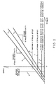
- plot line “a” reflects the maximum stimulus sensitivity of a stimulus responsive sensor while plot line “c” reflects the minimum stimulus sensitivity.
- Line “d” reflects the minimum realistic stimulus.
- the output at the maximum stimulus offset is shown at “e” and the output at the minimum stimulus output is shown at “f”.
- the output at "g” and “h” reflect the maximum and minimum excessive offset shift detection thresholds selected to avoid nuisance faults and to have maximum and minimum detection thresholds required to due to manufacturing tolerances.
- An example of a circuit made in accordance with the preceding description employs an analog ground voltage equal to 0.70 Vpwr.
- the partially signal conditioned signal which serves as the output stage inverting input, will nominally equal the analog ground following offset and gain compensation and at zero stimulus.
- a fault detecting circuit having a threshold of signals at the inverting input of the output stage greater than ⁇ 0.70 Vpwr- 0.05 Vpwr/Output stage voltage gain ⁇ will achieve detection of signals nominally 5% below the nominal output at zero stimulus following sensor calibration.
- a typical application may set the fault threshold at 3.667V plus a manufacturing tolerance of 10mV given Vpwr equal to 5.0V and an output stage voltage gain of-1.5V/V.
- Compensation for offset and gain enables the definition of the internal range of behavior of the electronics resulting in a known slope and offset of the conditioning signal and, in conjunction with pressure sensing applications, a reference voltage is selected to reflect zero absolute pressure, a pressure which can not be obtained.
- faults relating to a sense element electrical parameter such as 0.05 Vpwr/Output stage voltage gain, as well as faults in the conditioning electronics.
Landscapes
- Physics & Mathematics (AREA)
- General Physics & Mathematics (AREA)
- Measuring Fluid Pressure (AREA)
Abstract
Description
- This invention relates generally to the detection of excessive negative offset shift of a sensor signal, particularly, a signal conditioned sensor signal.
- Systems interpreting sensor outputs, herein simply called System, often can not detect if a sensor's output offset (i.e., sensor output at minimum stimulus input) has shifted negatively more than an acceptable amount due to one or both of the following:
- 1. The shifted sensor's output may be outside the System's input range, or
- 2. The sensor may clamp outputs below a certain level thereby masking the actual negative offset shift.
-
- An object of the invention is the provision of a sensor which overcomes the above noted prior art limitations. Another object is the provision of a method and apparatus for sensitively detecting negative offset shifts and providing a sensor output by the System indicative of a sensor fault. Yet another object is the provision of such a method and apparatus which provide detection of offset shifts due either to drift in the sensor per se or in the compensation of associated circuitry. Another object is the provision of a method and apparatus for sensitively detecting a negative offset shift of a piezoresistive Wheatstone sensor output and providing a sensor output by the System indicative of a fault.
- Briefly in accordance with the invention, the offset compensated signal within a signal conditioning circuit is compared to a reference voltage based on an unobtainable stimulus input condition to determine a fault status. In the event that the fault status is set, the output is driven to an output level interpreted by the System as a fault. The sensor electronic elements include a sense element coupled to an ASIC (application specific integrated circuit) having signal conditioning circuitry including offset and gain compensation.
- Although it is not necessary to compensate gain prior to the fault status comparison, superior negative offset drift detection sensitivity can be achieved by basing the comparison on a both offset and gain compensated signal due to ASIC tolerances (i.e., changes in ASIC gain may influence offset).
- Other objects, advantages and details of the novel and improved apparatus and method of the invention appear in the following description of the preferred embodiment of the invention, the detailed description referring to the drawings in which:
- Fig. 1 is a schematic diagram of a Wheatstone bridge sense element coupled to an ASIC in which is shown certain signal conditioning electronics, and an excessive negative offset shift detection circuit. The full Wheatstone bridge sense element outputs are inputs to the ASIC which provides offset compensation and gain compensation to yield an output with a specific output relation versus input stimulus.
- Fig. 2 is a plot of output vs. stimulus (e.g., pressure) and shows the variation in the output versus stimulus relation as well as the variation in the excessive negative offset shift detection circuit.
-
- A simplified circuit diagram showing one embodiment is shown in Fig. 1. A full Wheatstone
bridge 10 is shown as one form of a sensor element used for sensing a pressure stimulus to which the invention applies comprising piezoresistive resistors R1, R2 in one half bridge and R3, R4 in the other half bridge. The full Wheatstone bridge is the parallel connection of the two half bridges and the bridge is connected between a voltage supply VBRG and ground RTN and has first and second outputs INP, INM. Outputs INP, INM serve as inputs to an ASIC having signal conditioning circuitry including offset and gain compensation. As shown in Fig.1, ASIC inputs INP, INM are connected to a conventionaloffset compensation section 12 having a coarse adjustment 12a, a fineoffset adjustment section 12b, and ananalog ground 12c. Theoutput 14 ofsection 12 is connected to a conventionalgain compensation section 16 having a coarse gain setting 16a, a fine gain setting 16b andanalog ground 16c. - The output VX of
section 16 is connected to a selected voltage reference VREF1. The output of comparator Q1 is connected to a controllable switch such as FET M1. The compensated signal VX is also connected to resistor R5 which in turn is serially connected to the negative input to amplifier Q2. The positive input to amplifier Q2 is connected to a selected reference voltage VREF2 and the output of the amplifier is fed back to the negative input thereof through feedback resistor R6. The output of switch M1 is connected to the negative input of amplifier Q2. - In the circuit shown, compensation causes signal VX to equal an analog ground voltage at minimum input stimulus. A comparison between the voltage at VX and VREF1 determines the fault status. The reference voltage, VREF1 is equal to an analog voltage plus (for the circuit shown) a tolerance term delta, Δ. For the circuit shown, if the voltage VX exceeds a threshold value, VREF1, the output of Q1 will be a logic "1" which turns on controllable switch FET M1, which in turn pulls down the negative input to amplifier Q2 causing Q2 to drive the sensor output to the high supply rail, VPWR. The tolerance term delta, Δ, should be made as small as possible to maximize detection sensitivity without causing nuisance fault reporting. Although one specific embodiment has been shown, the invention relates to any sensor conditioning circuit that provides access to a voltage following offset trimming which is sufficiently within the supply rails to permit voltage comparisons between the offset corrected signal and a reference voltage between the initial offset corrected signal and supply rail.
- In Fig. 2, plot line "a" reflects the maximum stimulus sensitivity of a stimulus responsive sensor while plot line "c" reflects the minimum stimulus sensitivity. Line "d" reflects the minimum realistic stimulus. At zero stimulus the output at the maximum stimulus offset is shown at "e" and the output at the minimum stimulus output is shown at "f". The output at "g" and "h" reflect the maximum and minimum excessive offset shift detection thresholds selected to avoid nuisance faults and to have maximum and minimum detection thresholds required to due to manufacturing tolerances.
- An example of a circuit made in accordance with the preceding description employs an analog ground voltage equal to 0.70 Vpwr. The partially signal conditioned signal, which serves as the output stage inverting input, will nominally equal the analog ground following offset and gain compensation and at zero stimulus. A fault detecting circuit having a threshold of signals at the inverting input of the output stage greater than {0.70 Vpwr- 0.05 Vpwr/Output stage voltage gain} will achieve detection of signals nominally 5% below the nominal output at zero stimulus following sensor calibration. A typical application may set the fault threshold at 3.667V plus a manufacturing tolerance of 10mV given Vpwr equal to 5.0V and an output stage voltage gain of-1.5V/V.
- Compensation for offset and gain enables the definition of the internal range of behavior of the electronics resulting in a known slope and offset of the conditioning signal and, in conjunction with pressure sensing applications, a reference voltage is selected to reflect zero absolute pressure, a pressure which can not be obtained.
- It should be noted that the comparison between the voltage at VX and VREF1 is made prior to the output since the output is limited by certain factors, such as supply voltage and external load drive capability.
- Among the faults which can be detected by the invention are faults relating to a sense element electrical parameter, such as 0.05 Vpwr/Output stage voltage gain, as well as faults in the conditioning electronics.
- It will be understood that the invention can be used with sensors responsive to various stimuli in addition to pressure, such as acceleration and that the invention includes all modifications and equivalents of the described embodiment falling within the scope of the appended claims.
Claims (8)
- Apparatus for detection of excessive negative offset of a sensor comprising a sense element having a conditioning circuit with positive and negative power supply connections, an output node and connections to a sense element and capable of providing offset signal compensation comprising:a first comparator having a positive and a negative input and an output,a signal compensated by the offset and gain compensation circuits connected to the positive input of the comparator and a first reference voltage connected to the negative input of the comparator, the compensated signal also connected to a resistor which in turn is connected to the negative input of a second comparator,a controllable switch having an input connected to the output of the second comparator,the positive input of the second comparator connected to a second reference voltage and a feedback resistor connected between the output of the second comparator and the negative output thereof.
- Apparatus according to claim 1 in which the sense element comprises piezoresistive resistors.
- Apparatus according to claim 1 in which the sense element comprises a full Wheatstone bridge.
- Apparatus according to claim 1 in which the sense element is responsive to pressure and the first reference voltage is selected to provide an output indicative of zero absolute pressure.
- Apparatus according to claim 1 in which the controllable switch is an FET.
- Apparatus for detection of excessive negative offset of a sensor comprising a sense element, a signal conditioning circuit with positive and negative power supply connections, at least one output node and connections to the sense element, a comparator circuit for comparing a compensated sense element signal with a voltage reference signal whereby a sensor output indicative of a fault condition will be generated for a specific output polarity of the comparator circuit.
- A method for providing detection of excessive negative offset of a condition responsive sensor signal comprising the steps ofcompensating the signal for gain and offset,comparing the compensative sensor signal with a reference voltage selected to reflect an unobtainable condition; anddriving the compensated signal to a selected fault level when the compensated voltage exceeds the reference voltage.
- A method according to claim 7 in which the condition responsive sensor is responsive to pressure and the reference voltage is selected to indicate a sensed pressure of absolute zero.
Applications Claiming Priority (4)
| Application Number | Priority Date | Filing Date | Title |
|---|---|---|---|
| US23409200P | 2000-09-20 | 2000-09-20 | |
| US234092P | 2000-09-20 | ||
| US09/947,822 US6549138B2 (en) | 2000-09-20 | 2001-09-06 | Method and apparatus for providing detection of excessive negative offset of a sensor |
| US947822P | 2001-09-06 |
Publications (2)
| Publication Number | Publication Date |
|---|---|
| EP1213563A2 true EP1213563A2 (en) | 2002-06-12 |
| EP1213563A3 EP1213563A3 (en) | 2007-03-07 |
Family
ID=26927556
Family Applications (1)
| Application Number | Title | Priority Date | Filing Date |
|---|---|---|---|
| EP01307967A Withdrawn EP1213563A3 (en) | 2000-09-20 | 2001-09-19 | Method and apparatus for providing detection of excessive negative offset of a sensor |
Country Status (2)
| Country | Link |
|---|---|
| US (1) | US6549138B2 (en) |
| EP (1) | EP1213563A3 (en) |
Families Citing this family (5)
| Publication number | Priority date | Publication date | Assignee | Title |
|---|---|---|---|---|
| US6765391B2 (en) * | 2002-10-22 | 2004-07-20 | Texas Instruments Incorporated | Low cost asic architecture for safety critical applications monitoring an applied stimulus |
| DE102004056133B4 (en) * | 2004-02-20 | 2007-04-12 | Fraunhofer-Gesellschaft zur Förderung der angewandten Forschung e.V. | Method for detecting an offset drift in a Wheatstone measuring bridge |
| DE102004021863A1 (en) * | 2004-05-04 | 2005-12-01 | Infineon Technologies Ag | Sensor element for providing a sensor signal and method for operating a sensor element |
| US20060036481A1 (en) * | 2004-07-27 | 2006-02-16 | White Martin A | Electronic voter registration system and method |
| US20060284627A1 (en) * | 2005-06-17 | 2006-12-21 | Ford Greg E | Apparatus for correcting electrical signals |
Citations (3)
| Publication number | Priority date | Publication date | Assignee | Title |
|---|---|---|---|---|
| EP0723161A1 (en) | 1994-08-08 | 1996-07-24 | The Nippon Signal Co. Ltd. | Trouble monitor device for bridge circuit |
| DE19728381A1 (en) | 1997-07-03 | 1999-01-07 | Bosch Gmbh Robert | Method and circuit for monitoring the function of a sensor bridge |
| EP0967462A1 (en) | 1998-06-26 | 1999-12-29 | B. Braun Melsungen Ag | Bridge sensor and verification method |
Family Cites Families (5)
| Publication number | Priority date | Publication date | Assignee | Title |
|---|---|---|---|---|
| US4203324A (en) * | 1977-08-05 | 1980-05-20 | Joseph Baumoel | Sonic liquid level detector |
| JPS58189571A (en) * | 1982-04-28 | 1983-11-05 | West Electric Co Ltd | Ultrasonic range finding device |
| USRE33028E (en) * | 1983-07-12 | 1989-08-22 | Dresser Industries, Inc. | Electropneumatic transducer system |
| US4527583A (en) * | 1983-07-12 | 1985-07-09 | Dresser Industries, Inc. | Electropneumatic transducer system |
| US6353324B1 (en) * | 1998-11-06 | 2002-03-05 | Bridge Semiconductor Corporation | Electronic circuit |
-
2001
- 2001-09-06 US US09/947,822 patent/US6549138B2/en not_active Expired - Fee Related
- 2001-09-19 EP EP01307967A patent/EP1213563A3/en not_active Withdrawn
Patent Citations (3)
| Publication number | Priority date | Publication date | Assignee | Title |
|---|---|---|---|---|
| EP0723161A1 (en) | 1994-08-08 | 1996-07-24 | The Nippon Signal Co. Ltd. | Trouble monitor device for bridge circuit |
| DE19728381A1 (en) | 1997-07-03 | 1999-01-07 | Bosch Gmbh Robert | Method and circuit for monitoring the function of a sensor bridge |
| EP0967462A1 (en) | 1998-06-26 | 1999-12-29 | B. Braun Melsungen Ag | Bridge sensor and verification method |
Also Published As
| Publication number | Publication date |
|---|---|
| US6549138B2 (en) | 2003-04-15 |
| EP1213563A3 (en) | 2007-03-07 |
| US20020047716A1 (en) | 2002-04-25 |
Similar Documents
| Publication | Publication Date | Title |
|---|---|---|
| US6433554B1 (en) | Method and apparatus for in-range fault detection of condition responsive sensor | |
| US6518880B2 (en) | Physical-quantity detection sensor | |
| KR960006439B1 (en) | Circuit for converting analog signal into logic signal | |
| JP4296811B2 (en) | Physical quantity sensor device | |
| US5231351A (en) | Magnetoresistive speed sensor processing circuit utilizing a symmetrical hysteresis signal | |
| US6940290B2 (en) | Sensor output processing device having self-diagnosis function | |
| US20230314260A1 (en) | Method for Monitoring the Function of a Capacitive Pressure Measuring Cell | |
| JP2002311045A (en) | Acceleration sensor | |
| KR100422889B1 (en) | Pressure transducer, in particular for sensing a lateral collision in a motor vehicle | |
| JP2002174559A (en) | Physical quantity detector | |
| JP5278114B2 (en) | Sensor device | |
| US6549138B2 (en) | Method and apparatus for providing detection of excessive negative offset of a sensor | |
| JPH0777546A (en) | Current detector for control load and failure diagnostic unit employing it | |
| JP4711248B2 (en) | Method and apparatus for detecting excessive negative offset of a sensor | |
| JP2004144751A (en) | Wheatstone bridge conditioning circuit | |
| US20240235503A9 (en) | Physical quantity outputting circuit | |
| JP2737481B2 (en) | Semiconductor acceleration sensor | |
| US6181192B1 (en) | Constant voltage circuit comprising temperature dependent elements and a differential amplifier | |
| JP2001091373A (en) | Pressure sensor circuit | |
| JP2618822B2 (en) | Capacitance sensor | |
| US6188226B1 (en) | Electric potential sensor | |
| JPH10190463A (en) | Signal processing device | |
| JP4345207B2 (en) | Mechanical quantity detection sensor | |
| JP2001201413A (en) | Pressure sensor | |
| JP3888196B2 (en) | Sensor output characteristics adjustment method |
Legal Events
| Date | Code | Title | Description |
|---|---|---|---|
| PUAI | Public reference made under article 153(3) epc to a published international application that has entered the european phase |
Free format text: ORIGINAL CODE: 0009012 |
|
| AK | Designated contracting states |
Kind code of ref document: A2 Designated state(s): AT BE CH CY DE DK ES FI FR GB GR IE IT LI LU MC NL PT SE TR |
|
| AX | Request for extension of the european patent |
Free format text: AL;LT;LV;MK;RO;SI |
|
| PUAL | Search report despatched |
Free format text: ORIGINAL CODE: 0009013 |
|
| AK | Designated contracting states |
Kind code of ref document: A3 Designated state(s): AT BE CH CY DE DK ES FI FR GB GR IE IT LI LU MC NL PT SE TR |
|
| AX | Request for extension of the european patent |
Extension state: AL LT LV MK RO SI |
|
| RAP1 | Party data changed (applicant data changed or rights of an application transferred) |
Owner name: SENSATA TECHNOLOGIES, INC. |
|
| RIC1 | Information provided on ipc code assigned before grant |
Ipc: G01D 18/00 20060101ALI20070130BHEP Ipc: G01D 3/08 20060101AFI20020418BHEP |
|
| 17P | Request for examination filed |
Effective date: 20070606 |
|
| AKX | Designation fees paid |
Designated state(s): DE FR GB |
|
| 17Q | First examination report despatched |
Effective date: 20090915 |
|
| STAA | Information on the status of an ep patent application or granted ep patent |
Free format text: STATUS: THE APPLICATION IS DEEMED TO BE WITHDRAWN |
|
| 18D | Application deemed to be withdrawn |
Effective date: 20150313 |