EP1211766A2 - InGaAsP semiconductor laser device - Google Patents
InGaAsP semiconductor laser device Download PDFInfo
- Publication number
- EP1211766A2 EP1211766A2 EP01125890A EP01125890A EP1211766A2 EP 1211766 A2 EP1211766 A2 EP 1211766A2 EP 01125890 A EP01125890 A EP 01125890A EP 01125890 A EP01125890 A EP 01125890A EP 1211766 A2 EP1211766 A2 EP 1211766A2
- Authority
- EP
- European Patent Office
- Prior art keywords
- layer
- optical waveguide
- semiconductor laser
- laser device
- type
- Prior art date
- Legal status (The legal status is an assumption and is not a legal conclusion. Google has not performed a legal analysis and makes no representation as to the accuracy of the status listed.)
- Granted
Links
- 239000004065 semiconductor Substances 0.000 title claims abstract description 128
- 230000003287 optical effect Effects 0.000 claims abstract description 106
- 238000005253 cladding Methods 0.000 claims abstract description 68
- 229910001218 Gallium arsenide Inorganic materials 0.000 claims abstract description 54
- QAOWNCQODCNURD-UHFFFAOYSA-N Sulfuric acid Chemical compound OS(O)(=O)=O QAOWNCQODCNURD-UHFFFAOYSA-N 0.000 claims abstract description 48
- 239000000758 substrate Substances 0.000 claims abstract description 37
- VEXZGXHMUGYJMC-UHFFFAOYSA-N Hydrochloric acid Chemical compound Cl VEXZGXHMUGYJMC-UHFFFAOYSA-N 0.000 claims abstract description 30
- 238000000034 method Methods 0.000 claims abstract description 17
- 238000005530 etching Methods 0.000 claims description 49
- 230000002745 absorbent Effects 0.000 claims description 14
- 239000002250 absorbent Substances 0.000 claims description 14
- 238000009413 insulation Methods 0.000 claims description 9
- 238000002347 injection Methods 0.000 claims description 4
- 239000007924 injection Substances 0.000 claims description 4
- 238000010276 construction Methods 0.000 description 16
- 230000004888 barrier function Effects 0.000 description 8
- 239000011248 coating agent Substances 0.000 description 8
- 238000000576 coating method Methods 0.000 description 8
- 230000010355 oscillation Effects 0.000 description 8
- XAGFODPZIPBFFR-UHFFFAOYSA-N aluminium Chemical compound [Al] XAGFODPZIPBFFR-UHFFFAOYSA-N 0.000 description 7
- 229910052782 aluminium Inorganic materials 0.000 description 7
- 239000000203 mixture Substances 0.000 description 7
- 238000001459 lithography Methods 0.000 description 6
- 125000002524 organometallic group Chemical group 0.000 description 4
- 238000000927 vapour-phase epitaxy Methods 0.000 description 4
- 150000002500 ions Chemical class 0.000 description 3
- 238000004519 manufacturing process Methods 0.000 description 3
- 239000000463 material Substances 0.000 description 3
- 238000010521 absorption reaction Methods 0.000 description 2
- 239000000969 carrier Substances 0.000 description 2
- 239000013078 crystal Substances 0.000 description 2
- 230000003247 decreasing effect Effects 0.000 description 2
- 230000020169 heat generation Effects 0.000 description 2
- 230000031700 light absorption Effects 0.000 description 2
- 230000003647 oxidation Effects 0.000 description 2
- 238000007254 oxidation reaction Methods 0.000 description 2
- OAICVXFJPJFONN-UHFFFAOYSA-N Phosphorus Chemical compound [P] OAICVXFJPJFONN-UHFFFAOYSA-N 0.000 description 1
- 230000015572 biosynthetic process Effects 0.000 description 1
- 230000015556 catabolic process Effects 0.000 description 1
- 238000006243 chemical reaction Methods 0.000 description 1
- 238000006731 degradation reaction Methods 0.000 description 1
- 238000000151 deposition Methods 0.000 description 1
- 230000008021 deposition Effects 0.000 description 1
- 238000009792 diffusion process Methods 0.000 description 1
- 239000003814 drug Substances 0.000 description 1
- 238000005259 measurement Methods 0.000 description 1
- 238000001451 molecular beam epitaxy Methods 0.000 description 1
- 229910052698 phosphorus Inorganic materials 0.000 description 1
- 239000011574 phosphorus Substances 0.000 description 1
- 239000002994 raw material Substances 0.000 description 1
- 239000007787 solid Substances 0.000 description 1
- 239000000126 substance Substances 0.000 description 1
Images


Classifications
-
- H—ELECTRICITY
- H01—ELECTRIC ELEMENTS
- H01S—DEVICES USING THE PROCESS OF LIGHT AMPLIFICATION BY STIMULATED EMISSION OF RADIATION [LASER] TO AMPLIFY OR GENERATE LIGHT; DEVICES USING STIMULATED EMISSION OF ELECTROMAGNETIC RADIATION IN WAVE RANGES OTHER THAN OPTICAL
- H01S5/00—Semiconductor lasers
- H01S5/30—Structure or shape of the active region; Materials used for the active region
-
- H—ELECTRICITY
- H01—ELECTRIC ELEMENTS
- H01S—DEVICES USING THE PROCESS OF LIGHT AMPLIFICATION BY STIMULATED EMISSION OF RADIATION [LASER] TO AMPLIFY OR GENERATE LIGHT; DEVICES USING STIMULATED EMISSION OF ELECTROMAGNETIC RADIATION IN WAVE RANGES OTHER THAN OPTICAL
- H01S5/00—Semiconductor lasers
- H01S5/20—Structure or shape of the semiconductor body to guide the optical wave ; Confining structures perpendicular to the optical axis, e.g. index or gain guiding, stripe geometry, broad area lasers, gain tailoring, transverse or lateral reflectors, special cladding structures, MQW barrier reflection layers
- H01S5/22—Structure or shape of the semiconductor body to guide the optical wave ; Confining structures perpendicular to the optical axis, e.g. index or gain guiding, stripe geometry, broad area lasers, gain tailoring, transverse or lateral reflectors, special cladding structures, MQW barrier reflection layers having a ridge or stripe structure
- H01S5/223—Buried stripe structure
- H01S5/2231—Buried stripe structure with inner confining structure only between the active layer and the upper electrode
-
- B—PERFORMING OPERATIONS; TRANSPORTING
- B82—NANOTECHNOLOGY
- B82Y—SPECIFIC USES OR APPLICATIONS OF NANOSTRUCTURES; MEASUREMENT OR ANALYSIS OF NANOSTRUCTURES; MANUFACTURE OR TREATMENT OF NANOSTRUCTURES
- B82Y20/00—Nanooptics, e.g. quantum optics or photonic crystals
-
- H—ELECTRICITY
- H01—ELECTRIC ELEMENTS
- H01S—DEVICES USING THE PROCESS OF LIGHT AMPLIFICATION BY STIMULATED EMISSION OF RADIATION [LASER] TO AMPLIFY OR GENERATE LIGHT; DEVICES USING STIMULATED EMISSION OF ELECTROMAGNETIC RADIATION IN WAVE RANGES OTHER THAN OPTICAL
- H01S5/00—Semiconductor lasers
- H01S5/10—Construction or shape of the optical resonator, e.g. extended or external cavity, coupled cavities, bent-guide, varying width, thickness or composition of the active region
- H01S5/16—Window-type lasers, i.e. with a region of non-absorbing material between the active region and the reflecting surface
- H01S5/164—Window-type lasers, i.e. with a region of non-absorbing material between the active region and the reflecting surface with window regions comprising semiconductor material with a wider bandgap than the active layer
-
- H—ELECTRICITY
- H01—ELECTRIC ELEMENTS
- H01S—DEVICES USING THE PROCESS OF LIGHT AMPLIFICATION BY STIMULATED EMISSION OF RADIATION [LASER] TO AMPLIFY OR GENERATE LIGHT; DEVICES USING STIMULATED EMISSION OF ELECTROMAGNETIC RADIATION IN WAVE RANGES OTHER THAN OPTICAL
- H01S5/00—Semiconductor lasers
- H01S5/20—Structure or shape of the semiconductor body to guide the optical wave ; Confining structures perpendicular to the optical axis, e.g. index or gain guiding, stripe geometry, broad area lasers, gain tailoring, transverse or lateral reflectors, special cladding structures, MQW barrier reflection layers
- H01S5/2004—Confining in the direction perpendicular to the layer structure
-
- H—ELECTRICITY
- H01—ELECTRIC ELEMENTS
- H01S—DEVICES USING THE PROCESS OF LIGHT AMPLIFICATION BY STIMULATED EMISSION OF RADIATION [LASER] TO AMPLIFY OR GENERATE LIGHT; DEVICES USING STIMULATED EMISSION OF ELECTROMAGNETIC RADIATION IN WAVE RANGES OTHER THAN OPTICAL
- H01S5/00—Semiconductor lasers
- H01S5/30—Structure or shape of the active region; Materials used for the active region
- H01S5/34—Structure or shape of the active region; Materials used for the active region comprising quantum well or superlattice structures, e.g. single quantum well [SQW] lasers, multiple quantum well [MQW] lasers or graded index separate confinement heterostructure [GRINSCH] lasers
- H01S5/3403—Structure or shape of the active region; Materials used for the active region comprising quantum well or superlattice structures, e.g. single quantum well [SQW] lasers, multiple quantum well [MQW] lasers or graded index separate confinement heterostructure [GRINSCH] lasers having a strained layer structure in which the strain performs a special function, e.g. general strain effects, strain versus polarisation
-
- H—ELECTRICITY
- H01—ELECTRIC ELEMENTS
- H01S—DEVICES USING THE PROCESS OF LIGHT AMPLIFICATION BY STIMULATED EMISSION OF RADIATION [LASER] TO AMPLIFY OR GENERATE LIGHT; DEVICES USING STIMULATED EMISSION OF ELECTROMAGNETIC RADIATION IN WAVE RANGES OTHER THAN OPTICAL
- H01S5/00—Semiconductor lasers
- H01S5/30—Structure or shape of the active region; Materials used for the active region
- H01S5/34—Structure or shape of the active region; Materials used for the active region comprising quantum well or superlattice structures, e.g. single quantum well [SQW] lasers, multiple quantum well [MQW] lasers or graded index separate confinement heterostructure [GRINSCH] lasers
- H01S5/343—Structure or shape of the active region; Materials used for the active region comprising quantum well or superlattice structures, e.g. single quantum well [SQW] lasers, multiple quantum well [MQW] lasers or graded index separate confinement heterostructure [GRINSCH] lasers in AIIIBV compounds, e.g. AlGaAs-laser, InP-based laser
- H01S5/3434—Structure or shape of the active region; Materials used for the active region comprising quantum well or superlattice structures, e.g. single quantum well [SQW] lasers, multiple quantum well [MQW] lasers or graded index separate confinement heterostructure [GRINSCH] lasers in AIIIBV compounds, e.g. AlGaAs-laser, InP-based laser with a well layer comprising at least both As and P as V-compounds
-
- H—ELECTRICITY
- H01—ELECTRIC ELEMENTS
- H01S—DEVICES USING THE PROCESS OF LIGHT AMPLIFICATION BY STIMULATED EMISSION OF RADIATION [LASER] TO AMPLIFY OR GENERATE LIGHT; DEVICES USING STIMULATED EMISSION OF ELECTROMAGNETIC RADIATION IN WAVE RANGES OTHER THAN OPTICAL
- H01S5/00—Semiconductor lasers
- H01S5/30—Structure or shape of the active region; Materials used for the active region
- H01S5/34—Structure or shape of the active region; Materials used for the active region comprising quantum well or superlattice structures, e.g. single quantum well [SQW] lasers, multiple quantum well [MQW] lasers or graded index separate confinement heterostructure [GRINSCH] lasers
- H01S5/343—Structure or shape of the active region; Materials used for the active region comprising quantum well or superlattice structures, e.g. single quantum well [SQW] lasers, multiple quantum well [MQW] lasers or graded index separate confinement heterostructure [GRINSCH] lasers in AIIIBV compounds, e.g. AlGaAs-laser, InP-based laser
- H01S5/34346—Structure or shape of the active region; Materials used for the active region comprising quantum well or superlattice structures, e.g. single quantum well [SQW] lasers, multiple quantum well [MQW] lasers or graded index separate confinement heterostructure [GRINSCH] lasers in AIIIBV compounds, e.g. AlGaAs-laser, InP-based laser characterised by the materials of the barrier layers
- H01S5/34373—Structure or shape of the active region; Materials used for the active region comprising quantum well or superlattice structures, e.g. single quantum well [SQW] lasers, multiple quantum well [MQW] lasers or graded index separate confinement heterostructure [GRINSCH] lasers in AIIIBV compounds, e.g. AlGaAs-laser, InP-based laser characterised by the materials of the barrier layers based on InGa(Al)AsP
-
- H—ELECTRICITY
- H01—ELECTRIC ELEMENTS
- H01S—DEVICES USING THE PROCESS OF LIGHT AMPLIFICATION BY STIMULATED EMISSION OF RADIATION [LASER] TO AMPLIFY OR GENERATE LIGHT; DEVICES USING STIMULATED EMISSION OF ELECTROMAGNETIC RADIATION IN WAVE RANGES OTHER THAN OPTICAL
- H01S5/00—Semiconductor lasers
- H01S5/30—Structure or shape of the active region; Materials used for the active region
- H01S5/34—Structure or shape of the active region; Materials used for the active region comprising quantum well or superlattice structures, e.g. single quantum well [SQW] lasers, multiple quantum well [MQW] lasers or graded index separate confinement heterostructure [GRINSCH] lasers
- H01S5/343—Structure or shape of the active region; Materials used for the active region comprising quantum well or superlattice structures, e.g. single quantum well [SQW] lasers, multiple quantum well [MQW] lasers or graded index separate confinement heterostructure [GRINSCH] lasers in AIIIBV compounds, e.g. AlGaAs-laser, InP-based laser
- H01S5/34346—Structure or shape of the active region; Materials used for the active region comprising quantum well or superlattice structures, e.g. single quantum well [SQW] lasers, multiple quantum well [MQW] lasers or graded index separate confinement heterostructure [GRINSCH] lasers in AIIIBV compounds, e.g. AlGaAs-laser, InP-based laser characterised by the materials of the barrier layers
- H01S5/34386—Structure or shape of the active region; Materials used for the active region comprising quantum well or superlattice structures, e.g. single quantum well [SQW] lasers, multiple quantum well [MQW] lasers or graded index separate confinement heterostructure [GRINSCH] lasers in AIIIBV compounds, e.g. AlGaAs-laser, InP-based laser characterised by the materials of the barrier layers explicitly Al-free
Definitions
- the present invention relates to a semiconductor laser device having an end-facet window structure, and a process for producing such a semiconductor laser device.
- window structures are formed in the vicinities of end facets, i.e., crystals having a greater bandgap than an active layer are formed in the vicinities of the end facets, so as to prevent the light absorption in the vicinities of end facets.
- Kazushige Kawasaki et al. (“0.98 ⁇ m band ridge-type window structure semiconductor laser (1),” Digest 29a-PA-19, 1997 Spring JSAP Annual Meeting, The Japan Society of Applied Physics) disclose a semiconductor laser device in the 980 nm band, which has a window structure formed by injecting Si ions into end regions of a ridge structure and disordering an In 0.2 Ga 0.8 As quantum well by thermal diffusion.
- the process for producing the above semiconductor laser device is very complicated and long since the vicinities of end facets are required to be insulated by injection of H ions after the injection of the Si ions in the vicinity of the active layer in order to prevent a current flow in the vicinities of end facets.
- the reliability of the semiconductor laser device is decreased due to oxidation of aluminum.
- a window structure is formed by removing near-edge portions of the active layer and regrowing semiconductor layers in the near-edge portions, aluminum is exposed on the regrowth boundary. Therefore, the reliability of the semiconductor laser device is further decreased.
- An object of the present invention is to provide a semiconductor laser device which does not contain aluminum in an active layer, has a window structure being non-absorbent of light in vicinities of end facets, and is reliable in a wide output power range from low to high output power.
- Another object of the present invention is to provide a process which can produce, by a simple process, a semiconductor laser device which does not contain aluminum in an active layer, has a window structure being non-absorbent of light in vicinities of end facets, and is reliable in a wide output power range from low to high output power.
- each of the lower and upper cladding layers, the first and second lower optical waveguide layers, the upper optical waveguide layer, and the non-absorbent layer are assumed to have such a composition as to lattice-match with the active layer.
- the lattice matching is defined as follows.
- the first layer is lattice-matched with the second layer.
- the layer grown above the substrate is lattice-matched with the substrate.
- the first conductive type is different in polarity of carriers from the second conductive type. That is, when the first conductive type is p type, and the second conductive type is n type.
- the semiconductor laser device according to the first aspect of the present invention may also have one or any possible combination of the following additional features (i) to (v).
- the active layer and the tensile strain barrier layers satisfy the following inequalities, -0.25 nm ⁇ ⁇ a ⁇ da + 2 ⁇ b ⁇ db ⁇ 0.25 nm, where da and db are respectively the thicknesses of the active layer and each of the tensile strain barrier layers.
- each of the lower and upper cladding layers, the first and second lower optical waveguide layers, the upper optical waveguide layer, and the non-absorbent layer are assumed to have such a composition as to lattice-match with the active layer.
- the process according to the second aspect of the present invention may further comprise, between the steps (g) and (h), the steps of (m) forming a second cap layer made of GaAs, on the first cap layer; and (n) etching off near-edge portions of the second cap layer located in third vicinities of the two opposite end facets of the semiconductor laser device by using a sulfuric acid etchant so as to produce additional portions of the spaces.
- the second cap layer is used as a mask; and in the step (i), the second cap layer is etched off concurrently with the near-edge portions of the upper optical waveguide layer, the compressive strain active layer, and the second lower optical waveguide layer.
- FIGS. 1A to 1C are cross-sectional views of a semiconductor laser device as the first embodiment of the present invention.
- Fig. 1A shows a cross section parallel to the direction of light emitted from the semiconductor laser device
- Figs. 1B and 1C respectively show the A-A' and B-B' cross sections indicated in Fig. 1A.
- a plurality of semiconductor laser devices are concurrently manufactured on a semiconductor wafer of a substrate, and arranged side by side, a construction corresponding to only one semiconductor laser device is indicated in each of Figs. 1A to 1C for the sake of simplicity of illustration and better understanding.
- a resist is applied to the In 0.49 Ga 0.51 P cap layer 8, and predetermined stripe regions of the resist each having a width of about 40 micrometers and extending in the ⁇ 0 1 1> direction are removed by conventional lithography, where the locations of the stripe regions are determined so that the center of each of the stripe regions correspond to resonator surfaces of the plurality of semiconductor laser devices produced from the semiconductor wafer.
- the In 0.49 Ga 0.51 P cap layer 8 is etched with a hydrochloric acid etchant by using the remaining portions of the resist as a mask so that stripe areas of the In x2 Ga 1- x2 As 1-y2 P y2 first upper optical waveguide layer 7 are exposed (i.e., first stripe grooves are formed).
- the etching with the hydrochloric acid etchant automatically stops at the upper surface of the In x2 Ga 1-x2 As 1-y2 P y2 first upper optical waveguide layer 7.
- the remaining portions of the resist are removed, and the layered structure is etched with a sulfuric acid etchant until stripe areas of the In 0.49 Ga 0.51 P lower etching stop layer 4 are exposed.
- the etching with the sulfuric acid etchant automatically stops at the upper surface of the In 0.49 Ga 0.51 P lower etching stop layer 4.
- a p-type or i-type In x2 Ga 1-x2 As 1-y2 P y2 second upper optical waveguide layer 9, a p-type Al z1 Ga 1-z1 As first upper cladding layer 10, and a p-type GaAs first upper etching stop layer 11 having a thickness of about 10 nm are formed.
- an In 0.49 Ga 0.51 P second upper etching stop layer 12 having a thickness of about 10 nm, an n-type Al z2 Ga 1-z2 As current confinement layer 13 (z2>z1), and a GaAs cap layer 14 are formed.
- a resist is applied to the GaAs cap layer 14, and predetermined stripe regions of the resist each having a width of about 1 to 3 micrometers and extending in the ⁇ 011> direction (i.e., perpendicular to the above first stripe grooves) are removed.
- the GaAs cap layer 14 and the n-type Al z2 Ga 1-z2 As current confinement layer 13 are etched with a sulfuric acid etchant by using the remaining portions of the resist as a mask so that stripe areas of the In 0.49 Ga 0.51 P second upper etching stop layer 12 are exposed (i.e., second stripe grooves are formed).
- the etching with the sulfuric acid etchant automatically stops at the upper surface of the In 0.49 Ga 0.51 P second upper etching stop layer 12. Subsequently, the remaining portions of the resist are removed, and the stripe areas of the In 0.49 Ga 0.51 P second upper etching stop layer 12 are removed by etching with a hydrochloric acid etchant.
- a p-type Al z1 Ga 1-z1 As second upper cladding layer 15 and a p-type GaAs contact layer 16 are formed.
- a p electrode 17 is formed over the p-type GaAs contact layer 16, the exposed (opposite) surface of the substrate 1 is polished, and an n electrode 18 is formed on the polished surface of the substrate 1.
- the semiconductor wafer with the layered structure is cleaved at the positions of the end facets into laser array bars. Then, high-reflection coating and low-reflection coating are laid on the end facets of the laser array bars. Thereafter, the laser array bars are further cleaved into chips.
- the semiconductor laser device as the first embodiment of the present invention is obtained.
- the p-type Al z1 Ga 1-z1 As first upper cladding layer 10 is arranged to have such a thickness that oscillation in a fundamental transverse mode can be maintained even when the semiconductor laser device operates with high output power. That is, a difference in an equivalent refractive index between a portion of the active region under the second stripe groove and another portion of the active region which is not located under the second stripe groove is in a range from 1.5 X10 -3 to 7 X10 -3 .
- the n-type Al z1 Ga 1-z1 As lower cladding layer 2, the p-type Al z1 Ga 1-z1 As first upper cladding layer 10, and the p-type Al z1 Ga 1-z1 As second upper cladding layer 15 have such a composition as to have a greater bandgap than the n-type or i-type In x2 Ga 1-x2 As 1-y2 P y2 first lower optical waveguide layer 3, the In x2 Ga 1-x2 As 1-y2 P y2 first upper optical waveguide layer 7, and the p-type or i-type In x2 Ga 1- x2 As 1-y2 P y2 second upper optical waveguide layer 9 have.
- the n-type Al z1 Ga 1-z1 As lower cladding layer 2, the p-type Al z1 Ga 1-z1 As first upper cladding layer 10, and the p-type Al z1 Ga 1-z1 As second upper cladding layer 15 may be made of an InGaAlP or InGaAlAsP material which lattice-matches with the GaAs substrate 1.
- the thickness from the upper surface of the In 0.49 Ga 0.51 P cap layer 8 to the bottom of the i-type In x2 Ga 1-x2 As 1-y2 P y2 second lower optical waveguide layer 5 is removed, and the spaces produced by the removal are filled with the p-type or i-type In x2 Ga 1-x2 As 1-y2 P y2 second upper optical waveguide layer 9.
- the near-edge portions i.e., portions in vicinities of the end facets
- the near-edge portions may be removed as follows.
- a GaAs cap layer having a thickness of about 10 nm is formed on the In 0.49 Ga 0.51 P cap layer 8, and a resist is applied to the GaAs cap layer. Then, predetermined stripe regions of the resist each having a width of about 40 micrometers and extending in the ⁇ 0 1 1> direction are removed by conventional lithography, where the locations of the stripe regions are determined so that the center of each of the stripe regions correspond to resonator surfaces of the plurality of semiconductor laser devices produced from the semiconductor wafer.
- the GaAs cap layer is etched with a sulfuric acid etchant by using the remaining portions of the resist as a mask so that stripe areas of the In 0.49 Ga 0.51 P cap layer 8 are exposed. Then, the remaining portions of the resist are removed, and the In 0.49 Ga 0.51 P cap layer 8 is etched with a hydrochloric acid etchant by using the remaining portions of the GaAs cap layer as a mask so that stripe areas of the In x2 Ga 1-x2 As 1-y2 P y2 first upper optical waveguide layer 7 are exposed.
- the layered structure is etched with a sulfuric acid etchant so that the remaining portions of the GaAs cap layer are removed, and stripe areas of the In 0.49 Ga 0.51 P lower etching stop layer 4 are exposed.
- a sulfuric acid etchant it is possible to prevent deposition of organic substances or the like on a regrowth surface during the process for removing the near-edge portions.
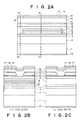
- Figs. 2A to 2C are cross-sectional views of a semiconductor laser device as a second embodiment of the present invention.
- Fig. 2A shows a cross section parallel to the direction of light emitted from the semiconductor laser device
- Figs. 2B and 2C respectively show the A-A' and B-B' cross sections indicated in Fig. 2A.
- a plurality of semiconductor laser devices are concurrently manufactured on a semiconductor wafer of a substrate, and arranged side by side, a construction corresponding to only one semiconductor laser device is indicated in each of Figs. 2A to 2C for the sake of simplicity of illustration and better understanding.
- the semiconductor laser device as the second embodiment of the present invention is different from the semiconductor laser device as the first embodiment of the present invention in only the formation of the contact layer as described below. Therefore, explanations of the same features as the first embodiment are not repeated.
- the p-type GaAs contact layer 16 stripe regions of the p-type GaAs contact layer 16 located above the aforementioned near-edge portions are removed, and the removed regions are covered with an insulation film 19. Subsequently, the p electrode 17 is formed over the remaining areas of the p-type GaAs contact layer 16 and the insulation film 19. Thereafter, the exposed (opposite) surface of the substrate 1 is polished, and the n electrode 18 is formed on the polished surface of the substrate 1.
- the current injected into the window structure can be greatly reduced. Therefore, the optical output power can be further increased.
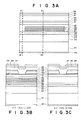
- FIGS. 3A to 3C are cross-sectional views of a semiconductor laser device as the third embodiment of the present invention.
- Fig. 3A shows a cross section parallel to the direction of light emitted from the semiconductor laser device
- Figs. 3B and 3C respectively show the A-A' and B-B' cross sections indicated in Fig. 3A.
- a plurality of semiconductor laser devices are concurrently manufactured on a semiconductor wafer of a substrate, and arranged side by side, a construction corresponding to only one semiconductor laser device is indicated in each of Figs. 3A to 3C for the sake of simplicity of illustration and better understanding.
- a resist is applied to the In 0.49 Ga 0.51 P cap layer 30, and predetermined stripe regions of the resist each having a width of about 40 micrometers and extending in the ⁇ 0 1 1> direction are removed by conventional lithography, where the locations of the stripe regions are determined so that the center of each of the stripe regions correspond to resonator surfaces of the plurality of semiconductor laser devices produced from the semiconductor wafer.
- the In 0.49 Ga 0.51 P cap layer 30 is etched with a hydrochloric acid etchant by using the remaining portions of the resist as a mask so that stripe areas of the In x2 Ga 1-x2 As 1-y2 P y2 first upper optical waveguide layer 29 are exposed (i.e., first stripe grooves are formed).
- the etching with the hydrochloric acid etchant automatically stops at the upper surface of the In x2 Ga 1-x2 As 1-y2 P y2 first upper optical waveguide layer 29.
- the remaining portions of the resist are removed, and the layered structure is etched with a sulfuric acid etchant until stripe areas of the In 0.49 Ga 0.51 P lower etching stop layer 24 are exposed.
- the etching with the sulfuric acid etchant automatically stops at the upper surface of the In 0.49 Ga 0.51 P lower etching stop layer 24.
- a p-type or i-type In x2 Ga 1-x2 As 1-y2 P y2 second upper optical waveguide layer 31 a p-type Al z1 Ga 1-z1 As first upper cladding layer 32, and a p-type GaAs first upper etching stop layer 33 having a thickness of about 10 nm are formed.
- an In 0.49 Ga 0.51 P second upper etching stop layer 34 having a thickness of about 10 nm, an n-type Al z2 Ga 1-z2 As current confinement layer 35 (z2>z1), and a GaAs cap layer 36 are formed.
- a resist is applied to the GaAs cap layer 36, and predetermined stripe regions of the resist each having a width of about 1 to 3 micrometers and extending in the ⁇ 011> direction (i.e., perpendicular to the above first stripe grooves) are removed.
- the GaAs cap layer 36 and the n-type Al z2 Ga 1-z2 As current confinement layer 35 are etched with a sulfuric acid etchant by using the remaining portions of the resist as a mask so that stripe areas of the In 0.49 Ga 0.51 P second upper etching stop layer 34 are exposed (i.e., second stripe grooves are formed).
- the etching with the sulfuric acid etchant automatically stops at the upper surface of the In 0.49 Ga 0.51 P second upper etching stop layer 34. Subsequently, the remaining portions of the resist are removed, and the stripe areas of the In 0.49 Ga 0.51 P second upper etching stop layer 34 are removed by etching with a hydrochloric acid etchant.
- a p-type Al z1 Ga 1-z1 As second upper cladding layer 37 and a p-type GaAs contact layer 38 are formed.
- a p electrode 39 is formed over the p-type GaAs contact layer 38, the exposed (opposite) surface of the substrate 21 is polished, and an n electrode 40 is formed on the polished surface of the substrate 21.
- the semiconductor wafer with the layered structure is cleaved at the positions of the end facets into laser array bars. Then, high-reflection coating and low-reflection coating are laid on the end facets of the laser array bars. Thereafter, the laser array bars are further cleaved into chips.
- the semiconductor laser device as the third embodiment of the present invention is obtained.
- the p-type Al z1 Ga 1-z1 As first upper cladding layer 32 is arranged to have such a thickness that oscillation in a fundamental transverse mode can be maintained even when the semiconductor laser device operates with high output power. That is, a difference in an equivalent refractive index between a portion of the active region under the second stripe groove and another portion of the active region which is not located under the second stripe groove is in a range from 1.5 X10 -3 to 7 X10 -3 .
- the n-type Al z1 Ga 1-z1 As lower cladding layer 22, the p-type Al z1 Ga 1-z1 As first upper cladding layer 32, and the p-type Al z1 Ga 1-z1 As second upper cladding layer 37 have such a composition as to have a greater bandgap than the n-type or i-type In x2 Ga 1-x2 As 1-y2 P y2 first lower optical waveguide layer 23, the In x2 Ga 1-x2 As 1-y2 P y2 first upper optical waveguide layer 29, and the p-type or i-type In x2 Ga 1- x2 As 1-y2 P y2 second upper optical waveguide layer 31 have.
- the n-type Al z1 Ga 1-z1 As lower cladding layer 22, the p-type Al z1 Ga 1-z1 As first upper cladding layer 32, and the p-type Al z1 Ga 1-z1 As second upper cladding layer 37 may be made of an InGaP, InGaAlP, or InGaAlAsP material which lattice-matches with the GaAs substrate 21.
- the thickness from the upper surface of the In 0.49 Ga 0.51 P cap layer 30 to the bottom of the i-type In x2 Ga 1-x2 As 1-y2 P y2 second lower optical waveguide layer 25 is removed, and the spaces produced by the removal are filled with the p-type or i-type In x2 Ga 1-x2 As 1-y2 P y2 second upper optical waveguide layer 31.
- the compressive strain quantum well active layer may include more than one quantum well.
- the absolute value of the sum of the product of the strain and the thickness of the compressive strain quantum well active layer and the product of the strain and the total thickness of the tensile strain barrier layers is equal to or smaller than 0.25 nm.
- the semiconductor laser device as the third embodiment of the present invention can emit laser light with high output power while maintaining the oscillation in a single transverse mode.
- the semiconductor laser device as the third embodiment is designed for oscillation in a single transverse mode
- the above process used for production of the semiconductor laser device as the third embodiment can also be applied to broad-stripe index-guided semiconductor laser devices each of which oscillates in multiple modes.
- FIGS. 4A to 4C are cross-sectional views of a semiconductor laser device as the fourth embodiment of the present invention.
- Fig. 4A shows a cross section parallel to the direction of light emitted from the semiconductor laser device
- Figs. 4B and 4C respectively show the A-A' and B-B' cross sections indicated in Fig. 4A.
- a plurality of semiconductor laser devices are concurrently manufactured on a semiconductor wafer of a substrate, and arranged side by side, a construction corresponding to only one semiconductor laser device is indicated in each of Figs. 4A to 4C for the sake of simplicity of illustration and better understanding.
- a resist is applied to the In 0.49 Ga 0.51 P cap layer 48, and predetermined stripe regions of the resist each having a width of about 40 micrometers and extending in the ⁇ 0 1 1> direction are removed by conventional lithography, where the locations of the stripe regions are determined so that the center of each of the stripe regions correspond to resonator surfaces of the plurality of semiconductor laser devices produced from the semiconductor wafer.
- the In 0.49 Ga 0.51 P cap layer 48 is etched with a hydrochloric acid etchant by using the remaining portions of the resist as a mask so that stripe areas of the In x2 Ga 1-x2 As 1-y2 P y2 first upper optical waveguide layer 47 are exposed (i.e., first stripe grooves are formed).
- the etching with the hydrochloric acid etchant automatically stops at the upper surface of the In x2 Ga 1-x2 As 1-y2 P y2 first upper optical waveguide layer 47.
- the remaining portions of the resist are removed, and the layered structure is etched with a sulfuric acid etchant until stripe areas of the In 0.49 Ga 0.51 P lower etching stop layer 44 are exposed.
- the etching with the sulfuric acid etchant automatically stops at the upper surface of the In 0.49 Ga 0.51 P lower etching stop layer 44.
- a p-type or i-type In x2 Ga 1-x2 As 1-y2 P y2 second upper optical waveguide layer 49, a p-type Al z1 Ga 1-z1 As first upper cladding layer 50, and a p-type In 0.49 Ga 0.51 P first upper etching stop layer 51 having a thickness of about 10 nm are formed.
- a p-type GaAs second upper etching stop layer 52 having a thickness of about 10 nm, an n-type In 0.49 Ga 0.51 P current confinement layer 53, and a GaAs cap layer 54 are formed.
- a resist is applied to the GaAs cap layer 54, and predetermined stripe regions of the resist each having a width of about 1 to 3 micrometers and extending in the ⁇ 011> direction (i.e., perpendicular to the above first stripe grooves) are removed.
- the GaAs cap layer 54 is etched with a sulfuric acid etchant by using the remaining portions of the resist as a mask so that stripe areas of the n-type In 0.49 Ga 0.51 P current confinement layer 53 are exposed.
- the etching with the sulfuric acid etchant automatically stops at the upper surface of the n-type In 0.49 Ga 0.51 P current confinement layer 53.
- a p-type Al z1 Ga 1-z1 As second upper cladding layer 55 and a p-type GaAs contact layer 56 are formed.
- a p electrode 57 is formed over the p-type GaAs contact layer 56, the exposed (opposite) surface of the substrate 41 is polished, and an n electrode 58 is formed on the polished surface of the substrate 41.
- the semiconductor wafer with the layered structure is cleaved at the positions of the end facets into laser array bars. Then, high-reflection coating and low-reflection coating are laid on the end facets of the laser array bars. Thereafter, the laser array bars are further cleaved into chips.
- the semiconductor laser device as the fourth embodiment of the present invention is obtained.
- the p-type Al z1 Ga 1-z1 As first upper cladding layer 50 is arranged to have such a composition and a thickness that oscillation in a fundamental transverse mode can be maintained even when the semiconductor laser device operates with high output power. That is, a difference in an equivalent refractive index between a portion of the active region under the second stripe groove and another portion of the active region which is not located under the second stripe groove is in a range from 1.5 X10 -3 to 7 X10 -3 .
- the n-type Al z1 Ga 1-z1 As lower cladding layer 42, the p-type Al z1 Ga 1-z1 As first upper cladding layer 50, and the p-type Al z1 Ga 1-z1 As second upper cladding layer 55 have such a composition as to have a greater bandgap than the n-type or i - type In x2 Ga 1-x2 As 1-y2 P y2 first lower optical waveguide layer 43, the In x2 Ga 1-x2 As 1-y2 P y2 first upper optical waveguide layer 47, and the p-type or i-type In x2 Ga 1- x2 As 1-y2 P y2 second upper optical waveguide layer 49 have.
- the n-type Al z1 Ga 1-z1 As lower cladding layer 42, the p-type Al z1 Ga 1-z1 As first upper cladding layer 50, and the p-type Al z1 Ga 1-z1 As second upper cladding layer 55 may be made of an InGaAlP or InGaAlAsP material which lattice-matches with the GaAs substrate 41.
- the thickness from the upper surface of the In 0.49 Ga 0.51 P cap layer 48 to the bottom of the i-type In x2 Ga 1-x2 As 1-y2 P y2 second lower optical waveguide layer 45 is removed, and the spaces produced by the removal are filled with the p-type or i-type In x2 Ga 1-x2 As 1-y2 P y2 second upper optical waveguide layer 49.
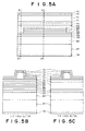
- FIGS. 5A to 5C are cross-sectional views of a semiconductor laser device as the fifth embodiment of the present invention.
- Fig. 5A shows a cross section parallel to the direction of light emitted from the semiconductor laser device
- Figs. 5B and 5C respectively show the A-A' and B-B' cross sections indicated in Fig. 5A.
- a plurality of semiconductor laser devices are concurrently manufactured on a semiconductor wafer of a substrate, and arranged side by side, a construction corresponding to only one semiconductor laser device is indicated in each of Figs. 5A to 5C for the sake of simplicity of illustration and better understanding.
- an n-type Al z1 Ga 1-z1 As lower cladding layer 62, an n-type or i-type (intrinsic) In x2 Ga 1-x2 As 1-y2 P y2 first lower optical waveguide layer 63 (0 ⁇ x2 ⁇ 0.3, x2 0.49y2), an i-type In 0.49 Ga 0.51 P lower etching stop layer 64 having a thickness of about 5 nm, an i-type In x2 Ga 1-x2 As 1-y2 P y2 second lower optical waveguide layer 65 having a thickness of about 10 nm, an In x1 Ga 1-x1 As 1-y1 P y1 compressive strain quantum well active layer 66 (0 ⁇ x1 ⁇ 0.4, 0 ⁇ y1 ⁇ 0.1), a p-type or i-type In x2 Ga 1-x2 As 1-y2 P y2 first upper optical waveguide layer 67 having a thickness of about 10 nm, and an In 0.49 Ga 0.51 P cap
- a resist is applied to the In 0.49 Ga 0.51 P cap layer 68, and predetermined stripe regions of the resist each having a width of about 40 micrometers and extending in the ⁇ 0 1 1> direction are removed by conventional lithography, where the locations of the stripe regions are determined so that the center of each of the stripe regions correspond to resonator surfaces of the plurality of semiconductor laser devices produced from the semiconductor wafer.
- the In 0.49 Ga 0.51 P cap layer 68 is etched with a hydrochloric acid etchant by using the remaining portions of the resist as a mask so that stripe areas of the In x2 Ga 1-x2 As 1-y2 P y2 first upper optical waveguide layer 67 are exposed (i.e., first stripe grooves are formed).
- the etching with the hydrochloric acid etchant automatically stops at the upper surface of the In x2 Ga 1-x2 As 1-y2 P y2 first upper optical waveguide layer 67.
- the remaining portions of the resist are removed, and the layered structure is etched with a sulfuric acid etchant until stripe areas of the In 0.49 Ga 0.51 P lower etching stop layer 64 are exposed.
- the etching with the sulfuric acid etchant automatically stops at the upper surface of the In 0.49 Ga 0.51 P lower etching stop layer 64.
- an insulation film is formed on the GaAs contact layer 73, and the insulation film except for predetermined stripe regions each having a width of about 1 to 3 micrometers and extending in the ⁇ 011> direction (i.e., perpendicular to the above first stripe grooves) is removed.
- the GaAs contact layer 73 and the p-type Al z1 Ga 1-z1 As second upper cladding layer 72 are etched with a sulfuric acid etchant by using the remaining portions of the insulation film as a mask so that a ridge is formed.
- another insulation film 74 is formed over the layered structure formed as above, and the insulation films on the top of the ridge are removed by conventional lithography.
- a p electrode 75 is formed over the layered structure formed above, the exposed (opposite) surface of the substrate 61 is polished, and an n electrode 76 is formed on the polished surface of the substrate 61.
- the semiconductor wafer with the layered structure is cleaved at the positions of the end facets into laser array bars. Then, high-reflection coating and low-reflection coating are laid on the end facets of the laser array bars. Thereafter, the laser array bars are further cleaved into chips.
- the semiconductor laser device as the fifth embodiment of the present invention is obtained.
- the p-type Al z1 Ga 1-z1 As first upper cladding layer 70 is arranged to have such a thickness that oscillation in a fundamental transverse mode can be maintained even when the semiconductor laser device operates with high output power. That is, a difference in an equivalent refractive index between a portion of the active region under the ridge and another portion of the active region which is not located under the ridge is in a range from 1.5 X10 -3 to 7 X10 -3 .
- the thickness from the upper surface of the In 0.49 Ga 0.51 P cap layer 68 to the bottom of the i-type In x2 Ga 1-x2 As 1-y2 P y2 second lower optical waveguide layer 65 is removed, and the spaces produced by the removal are filled with the p-type or i-type In x2 Ga 1-x2 As 1-y2 P y2 second upper optical waveguide layer 69.
- the semiconductor laser devices according to the present invention is reliable in operation with high output power, the semiconductor laser devices according to the present invention can be used as a light source for exciting a solid-state laser element or a wavelength conversion element.
Landscapes
- Physics & Mathematics (AREA)
- Optics & Photonics (AREA)
- Nanotechnology (AREA)
- Engineering & Computer Science (AREA)
- Chemical & Material Sciences (AREA)
- General Physics & Mathematics (AREA)
- Electromagnetism (AREA)
- Condensed Matter Physics & Semiconductors (AREA)
- Life Sciences & Earth Sciences (AREA)
- Biophysics (AREA)
- Crystallography & Structural Chemistry (AREA)
- Geometry (AREA)
- Semiconductor Lasers (AREA)
Abstract
Description
Claims (7)
- A semiconductor laser device comprising:a GaAs substrate of a first conductive type;a lower cladding layer of said first conductive type, formed on said GaAs substrate;a first lower optical waveguide layer made of Inx2Ga1-x2As1-y2Py2 having a first bandgap, and formed on said lower cladding layer, where 0≤x2≤0.3 and x2=0.49y2;an intermediate layer made of Inx5Ga1-x5P and formed on said first lower optical waveguide layer, where 0<x5<1;a second lower optical waveguide layer made of Inx2Ga1-x2As1-y2Py2 having said first bandgap, and formed on said intermediate layer except for near-edge areas of said first intermediate layer located in first vicinities of opposite end facets of said semiconductor laser device so as to leave first portions of spaces in the first vicinities of opposite end facets, where 0 ≤ x2 ≤ 0.3 and x2=0.49y2;a compressive strain active layer made of Inx1Ga1-x1As1-y1Py1 having a second bandgap smaller than said first bandgap, and formed on said second lower optical waveguide layer so as to leave second portions of said spaces in second vicinities of opposite end facets, where 0<x1≤0.4 and 0≤y1≤0.1;an upper optical waveguide layer made of Inx2Ga1- x2As1-y2Py2 having said first bandgap, and formed on said compressive strain active layer so as to leave third portions of said spaces in third vicinities of opposite end facets, where 0≤x2≤0.3 and x2=0.49y2;a cap layer made of Inx5Ga1-x5P and formed on said upper optical waveguide layer so as to leave fourth portions of said spaces in fourth vicinities of opposite end facets, where 0<x5<1;a non-absorbent layer made of Inx6Ga1-x6As1-y6Py6 having a third bandgap greater than said second bandgap, and formed over said cap layer so that said spaces are filled with the non-absorbent layer, where 0 ≤x6≤0.3 and x6=0.49y6;an upper cladding layer of a second conductive type, formed on said non-absorbent layer; anda contact layer of said second conductive type, formed on said upper cladding layer.
- A semiconductor laser device according to claim 1, wherein said contact layer is formed on said upper cladding layer except for near-edge areas of said upper cladding layer located in fifth vicinities of said end facets of said semiconductor laser device, and an insulation layer is formed on said near-edge areas of said upper cladding layer so as to prevent current injection through the near-edge areas of said upper cladding layer.
- A semiconductor laser device according to claim 1, wherein each of said lower and upper cladding layers is made of one of Alz1Ga1-z1As and Inx3(Alz3Ga1-z3)1-x3As1-y3Py3, where 0.2≤z1≤0.8, x3=0.49y3, 0.9<y3≤1, and 0≤z3≤1.
- A semiconductor laser device according to claim 1, wherein regions of said semiconductor laser device above at least a mid-thickness of said upper cladding layer except for a stripe region of said semiconductor laser device are removed so as to form a ridge and realize index guidance of light.
- A semiconductor laser device according to claim 1, further comprising a current confinement layer made of one of Alz2Ga1-z2As and In0.49Ga0.51P which lattice-match with GaAs, and formed above said upper optical waveguide layer so as to form an internal current confinement structure realizing index guidance of light, where 0.2<z2<1.
- A process for producing a semiconductor light emitting device, comprising the steps of:(a) forming above a GaAs substrate of a first conductive type a lower cladding layer of the first conductive type;(b) forming above said lower cladding layer a first lower optical waveguide layer made of Inx2Ga1-x2As1-y2Py2, where 0≤x2≤0.3 and x2=0.49y2;(c) forming above said first lower optical waveguide layer an intermediate layer made of Inx5Ga1-x5P, where 0<x5<1;(d) forming above said intermediate layer a second lower optical waveguide layer made of Inx2Ga1-x2As1-y2Py2, where 0≤x2≤0.3 and x2=0.49y2;(e) forming above said second lower optical waveguide layer a compressive strain active layer made of Inx1Ga1-x1As1-y1Py1, where 0<x1≤0.4 and 0≤y1≤0.1;(f) forming above said compressive strain active layer a first upper optical waveguide layer made of Inx2Ga1- x2As1-y2Py2, where 0≤x2≤0.3 and x2=0.49y2;(g) forming above said first upper optical waveguide layer a first cap layer made of Inx5Ga1-x5P, where 0<x5<1;(h) etching off near-edge portions of said first cap layer located in first vicinities of two opposite end facets of said semiconductor laser device with a hydrochloric acid etchant so as to produce first portions of spaces in the first vicinities of said two opposite end facets of said semiconductor laser device;(i) etching off near-edge portions of said upper optical waveguide layer, said compressive strain active layer, and said second lower optical waveguide layer, located in second vicinities of said two opposite end facets of said semiconductor laser device, by using a sulfuric acid etchant and said first cap layer as a mask, so as to produce second portions of said spaces in second vicinities of two opposite end facets of said semiconductor laser device;(j) forming a second upper optical waveguide layer made of Inx2Ga1-x2As1-y2Py2 over said first cap layer so that said spaces are filed with the second upper optical waveguide layer, where 0≤x2≤0.3 and x2=0.49y2;(k) forming an upper cladding layer of a second conductive type over said second upper optical waveguide layer; and(l) forming a GaAs contact layer of said second conductive type above said upper cladding layer.
- A process according to claim 6, further comprising, between said steps (g) and (h), the steps of:(m) forming a second cap layer made of GaAs, on said first cap layer; and(n) etching off near-edge portions of said second cap layer located in third vicinities of said two opposite end facets of said semiconductor laser device by using a sulfuric acid etchant so as to produce additional portions of said spaces;in said step (h), said second cap layer is used as a mask; andin said step (i), said second cap layer is etched off concurrently with said near-edge portions of said upper optical waveguide layer, said compressive strain active layer, and said second lower optical waveguide layer.
Applications Claiming Priority (2)
| Application Number | Priority Date | Filing Date | Title |
|---|---|---|---|
| JP2000331657 | 2000-10-31 | ||
| JP2000331657A JP2002141610A (en) | 2000-10-31 | 2000-10-31 | Semiconductor laser element and its fabricating method |
Publications (3)
| Publication Number | Publication Date |
|---|---|
| EP1211766A2 true EP1211766A2 (en) | 2002-06-05 |
| EP1211766A3 EP1211766A3 (en) | 2004-01-14 |
| EP1211766B1 EP1211766B1 (en) | 2006-01-25 |
Family
ID=18807968
Family Applications (1)
| Application Number | Title | Priority Date | Filing Date |
|---|---|---|---|
| EP01125890A Expired - Lifetime EP1211766B1 (en) | 2000-10-31 | 2001-10-30 | InGaAsP semiconductor laser device |
Country Status (5)
| Country | Link |
|---|---|
| US (1) | US6546033B2 (en) |
| EP (1) | EP1211766B1 (en) |
| JP (1) | JP2002141610A (en) |
| KR (1) | KR100771082B1 (en) |
| DE (1) | DE60116827T2 (en) |
Cited By (1)
| Publication number | Priority date | Publication date | Assignee | Title |
|---|---|---|---|---|
| EP1263100A3 (en) * | 2001-05-28 | 2005-02-09 | Fuji Photo Film Co., Ltd. | Semiconductor laser device and method of manufacture thereof |
Families Citing this family (7)
| Publication number | Priority date | Publication date | Assignee | Title |
|---|---|---|---|---|
| US6580738B2 (en) * | 1999-12-08 | 2003-06-17 | Fuji Photo Film Co., Ltd. | High-power semiconductor laser device in which near-edge portions of active layer are removed |
| EP1583187B1 (en) * | 2000-10-12 | 2007-07-04 | FUJIFILM Corporation | Semiconductor laser device with a current non-injection region near a resonator end face |
| JP2002305352A (en) * | 2001-04-05 | 2002-10-18 | Fuji Photo Film Co Ltd | Semiconductor laser element |
| JP2003069148A (en) * | 2001-08-27 | 2003-03-07 | Fuji Photo Film Co Ltd | Semiconductor laser device |
| US20030235225A1 (en) * | 2002-06-22 | 2003-12-25 | Rick Glew | Guided self-aligned laser structure with integral current blocking layer |
| KR100785772B1 (en) * | 2005-12-08 | 2007-12-18 | 한국전자통신연구원 | Semiconductor laser diode using change of energy band structure |
| US11824322B2 (en) * | 2021-02-16 | 2023-11-21 | Ii-Vi Delaware, Inc. | Laser device with non-absorbing mirror, and method |
Family Cites Families (7)
| Publication number | Priority date | Publication date | Assignee | Title |
|---|---|---|---|---|
| US4802182A (en) * | 1987-11-05 | 1989-01-31 | Xerox Corporation | Monolithic two dimensional waveguide coupled cavity laser/modulator |
| JP3183683B2 (en) * | 1991-09-06 | 2001-07-09 | シャープ株式会社 | Window type semiconductor laser device |
| US5412678A (en) * | 1992-09-22 | 1995-05-02 | Xerox Corporation | Multi-beam, orthogonally-polarized emitting monolithic quantum well lasers |
| JP3714430B2 (en) * | 1996-04-15 | 2005-11-09 | シャープ株式会社 | Distributed feedback semiconductor laser device |
| RO116694B1 (en) * | 1997-06-09 | 2001-04-30 | Iulian Basarab Petrescu-Prahova | Diode-like high power laser-effect device and process for making the same |
| JP3317335B2 (en) * | 1998-02-10 | 2002-08-26 | 富士写真フイルム株式会社 | Semiconductor laser device |
| JP2000031585A (en) * | 1998-07-15 | 2000-01-28 | Rohm Co Ltd | Semiconductor laser device |
-
2000
- 2000-10-31 JP JP2000331657A patent/JP2002141610A/en not_active Withdrawn
-
2001
- 2001-10-24 KR KR1020010065584A patent/KR100771082B1/en not_active Expired - Fee Related
- 2001-10-30 EP EP01125890A patent/EP1211766B1/en not_active Expired - Lifetime
- 2001-10-30 DE DE60116827T patent/DE60116827T2/en not_active Expired - Lifetime
- 2001-10-31 US US09/984,852 patent/US6546033B2/en not_active Expired - Fee Related
Cited By (1)
| Publication number | Priority date | Publication date | Assignee | Title |
|---|---|---|---|---|
| EP1263100A3 (en) * | 2001-05-28 | 2005-02-09 | Fuji Photo Film Co., Ltd. | Semiconductor laser device and method of manufacture thereof |
Also Published As
| Publication number | Publication date |
|---|---|
| US20020051477A1 (en) | 2002-05-02 |
| EP1211766B1 (en) | 2006-01-25 |
| DE60116827D1 (en) | 2006-04-13 |
| DE60116827T2 (en) | 2006-11-02 |
| EP1211766A3 (en) | 2004-01-14 |
| JP2002141610A (en) | 2002-05-17 |
| KR20020033524A (en) | 2002-05-07 |
| KR100771082B1 (en) | 2007-10-29 |
| US6546033B2 (en) | 2003-04-08 |
Similar Documents
| Publication | Publication Date | Title |
|---|---|---|
| JPH11220224A (en) | Semiconductor laser | |
| US6580738B2 (en) | High-power semiconductor laser device in which near-edge portions of active layer are removed | |
| US6396863B1 (en) | High-power semiconductor laser device having index-guided structure with InAlGaP current confinement layer | |
| EP1211766B1 (en) | InGaAsP semiconductor laser device | |
| EP1220393B1 (en) | Semiconductor laser device having InGaAs compressive-strain active layer, GaAsP tensile-strain barrier layers and InGaP optical waveguide layers | |
| US6400743B1 (en) | High-power semiconductor laser device having current confinement structure and index-guided structure | |
| JP3859839B2 (en) | Refractive index semiconductor laser device | |
| US6621845B2 (en) | Semiconductor laser device which includes AlGaAs optical waveguide layer being formed over internal stripe groove and having controlled refractive index | |
| US6973109B2 (en) | Semiconductor laser device having strain buffer layer between compressive-strain quantum well layer and tensile-strain barrier layer | |
| US6856636B2 (en) | Semiconductor laser device | |
| US20010017871A1 (en) | High-power semiconductor laser device in which near-edge portions of active layer are removed | |
| US6816524B2 (en) | InGaAsP or InGaAs semiconductor laser element in which near-edge portion of active layer is substituted with GaAs optical waveguide layer having greater bandgap than active layer | |
| US6600770B2 (en) | High-power semiconductor laser device having current confinement structure and index-guided structure and stably oscillating in single mode | |
| US6795469B2 (en) | Semiconductor laser element | |
| JP2001223436A (en) | Semiconductor laser device | |
| US6873637B2 (en) | Semiconductor laser element including optical waveguide layers which have gradually varying bandgaps so as to reduce electrical resistance at interfaces | |
| JP2001053382A (en) | Semiconductor laser | |
| EP1251609B1 (en) | High-power semiconductor window laser device | |
| EP1263100A2 (en) | Semiconductor laser device and method of manufacture thereof | |
| JP2003198066A (en) | Semiconductor laser device | |
| JP2001267689A (en) | Semiconductor laser element | |
| JP2003142782A (en) | Semiconductor laser element | |
| JP2001053383A (en) | Semiconductor laser and manufacture thereof | |
| JP2001053390A (en) | Semiconductor laser and manufacture thereof | |
| JP2003069157A (en) | Semiconductor laser element |
Legal Events
| Date | Code | Title | Description |
|---|---|---|---|
| PUAI | Public reference made under article 153(3) epc to a published international application that has entered the european phase |
Free format text: ORIGINAL CODE: 0009012 |
|
| AK | Designated contracting states |
Kind code of ref document: A2 Designated state(s): AT BE CH CY DE DK ES FI FR GB GR IE IT LI LU MC NL PT SE TR |
|
| AX | Request for extension of the european patent |
Free format text: AL;LT;LV;MK;RO;SI |
|
| PUAL | Search report despatched |
Free format text: ORIGINAL CODE: 0009013 |
|
| AK | Designated contracting states |
Kind code of ref document: A3 Designated state(s): AT BE CH CY DE DK ES FI FR GB GR IE IT LI LU MC NL PT SE TR |
|
| AX | Request for extension of the european patent |
Extension state: AL LT LV MK RO SI |
|
| 17P | Request for examination filed |
Effective date: 20040302 |
|
| 17Q | First examination report despatched |
Effective date: 20040428 |
|
| AKX | Designation fees paid |
Designated state(s): CH DE FR GB LI |
|
| GRAP | Despatch of communication of intention to grant a patent |
Free format text: ORIGINAL CODE: EPIDOSNIGR1 |
|
| GRAS | Grant fee paid |
Free format text: ORIGINAL CODE: EPIDOSNIGR3 |
|
| GRAA | (expected) grant |
Free format text: ORIGINAL CODE: 0009210 |
|
| AK | Designated contracting states |
Kind code of ref document: B1 Designated state(s): CH DE FR GB LI |
|
| REG | Reference to a national code |
Ref country code: GB Ref legal event code: FG4D |
|
| REG | Reference to a national code |
Ref country code: CH Ref legal event code: EP |
|
| REF | Corresponds to: |
Ref document number: 60116827 Country of ref document: DE Date of ref document: 20060413 Kind code of ref document: P |
|
| REG | Reference to a national code |
Ref country code: CH Ref legal event code: NV Representative=s name: BOVARD AG PATENTANWAELTE |
|
| ET | Fr: translation filed | ||
| PLBE | No opposition filed within time limit |
Free format text: ORIGINAL CODE: 0009261 |
|
| STAA | Information on the status of an ep patent application or granted ep patent |
Free format text: STATUS: NO OPPOSITION FILED WITHIN TIME LIMIT |
|
| 26N | No opposition filed |
Effective date: 20061026 |
|
| REG | Reference to a national code |
Ref country code: GB Ref legal event code: 732E |
|
| REG | Reference to a national code |
Ref country code: CH Ref legal event code: PFA Owner name: FUJI PHOTO FILM CO., LTD. Free format text: FUJI PHOTO FILM CO., LTD.#210 NAKANUMA,#MINAMI-ASHIGARA-SHI, KANAGAWA-KEN (JP) -TRANSFER TO- FUJI PHOTO FILM CO., LTD.#210 NAKANUMA,#MINAMI-ASHIGARA-SHI, KANAGAWA-KEN (JP) |
|
| REG | Reference to a national code |
Ref country code: CH Ref legal event code: PFA Owner name: FUJIFILM HOLDINGS CORPORATION Free format text: FUJI PHOTO FILM CO., LTD.#210 NAKANUMA,#MINAMI-ASHIGARA-SHI, KANAGAWA-KEN (JP) -TRANSFER TO- FUJIFILM HOLDINGS CORPORATION#210 NAKANUMA,#MINAMI-ASHIGARA-SHI, KANAGAWA-KEN (JP) Ref country code: CH Ref legal event code: PUE Owner name: FUJIFILM CORPORATION Free format text: FUJIFILM HOLDINGS CORPORATION#210 NAKANUMA,#MINAMI-ASHIGARA-SHI, KANAGAWA-KEN (JP) -TRANSFER TO- FUJIFILM CORPORATION#26-30, NISHIAZABU 2-CHOME MINATO-KU#TOKYO (JP) |
|
| REG | Reference to a national code |
Ref country code: CH Ref legal event code: PUE Owner name: NICHIA CORPORATION Free format text: FUJIFILM CORPORATION#26-30, NISHIAZABU 2-CHOME MINATO-KU#TOKYO (JP) -TRANSFER TO- NICHIA CORPORATION#491 OKA, KAMINAKA-CHO ANAN-SHI#TOKUSHIMA 774-8601 (JP) |
|
| REG | Reference to a national code |
Ref country code: DE Ref legal event code: R082 Ref document number: 60116827 Country of ref document: DE Representative=s name: KLUNKER, SCHMITT-NILSON, HIRSCH, DE |
|
| REG | Reference to a national code |
Ref country code: CH Ref legal event code: NV Representative=s name: BOVARD AG |
|
| REG | Reference to a national code |
Ref country code: DE Ref legal event code: R082 Ref document number: 60116827 Country of ref document: DE Representative=s name: KLUNKER, SCHMITT-NILSON, HIRSCH, DE Effective date: 20120521 Ref country code: DE Ref legal event code: R081 Ref document number: 60116827 Country of ref document: DE Owner name: NICHIA CORP., ANAN-SHI, JP Free format text: FORMER OWNER: FUJIFILM CORP., TOKIO/TOKYO, JP Effective date: 20120521 |
|
| REG | Reference to a national code |
Ref country code: GB Ref legal event code: 732E Free format text: REGISTERED BETWEEN 20120621 AND 20120627 |
|
| REG | Reference to a national code |
Ref country code: FR Ref legal event code: TP Owner name: NICHIA CORPORATION, JP Effective date: 20120806 Ref country code: FR Ref legal event code: CD Owner name: NICHIA CORPORATION, JP Effective date: 20120806 |
|
| PGFP | Annual fee paid to national office [announced via postgrant information from national office to epo] |
Ref country code: FR Payment date: 20121018 Year of fee payment: 12 Ref country code: CH Payment date: 20121012 Year of fee payment: 12 |
|
| PGFP | Annual fee paid to national office [announced via postgrant information from national office to epo] |
Ref country code: GB Payment date: 20131030 Year of fee payment: 13 |
|
| REG | Reference to a national code |
Ref country code: CH Ref legal event code: PL |
|
| PG25 | Lapsed in a contracting state [announced via postgrant information from national office to epo] |
Ref country code: CH Free format text: LAPSE BECAUSE OF NON-PAYMENT OF DUE FEES Effective date: 20131031 Ref country code: LI Free format text: LAPSE BECAUSE OF NON-PAYMENT OF DUE FEES Effective date: 20131031 |
|
| REG | Reference to a national code |
Ref country code: FR Ref legal event code: ST Effective date: 20140630 |
|
| PG25 | Lapsed in a contracting state [announced via postgrant information from national office to epo] |
Ref country code: FR Free format text: LAPSE BECAUSE OF NON-PAYMENT OF DUE FEES Effective date: 20131031 |
|
| PGFP | Annual fee paid to national office [announced via postgrant information from national office to epo] |
Ref country code: DE Payment date: 20141023 Year of fee payment: 14 |
|
| GBPC | Gb: european patent ceased through non-payment of renewal fee |
Effective date: 20141030 |
|
| PG25 | Lapsed in a contracting state [announced via postgrant information from national office to epo] |
Ref country code: GB Free format text: LAPSE BECAUSE OF NON-PAYMENT OF DUE FEES Effective date: 20141030 |
|
| REG | Reference to a national code |
Ref country code: DE Ref legal event code: R119 Ref document number: 60116827 Country of ref document: DE |
|
| PG25 | Lapsed in a contracting state [announced via postgrant information from national office to epo] |
Ref country code: DE Free format text: LAPSE BECAUSE OF NON-PAYMENT OF DUE FEES Effective date: 20160503 |