EP1211764A2 - System for optically pumping a long wavelength laser using a short wavelength laser - Google Patents
System for optically pumping a long wavelength laser using a short wavelength laser Download PDFInfo
- Publication number
- EP1211764A2 EP1211764A2 EP01114657A EP01114657A EP1211764A2 EP 1211764 A2 EP1211764 A2 EP 1211764A2 EP 01114657 A EP01114657 A EP 01114657A EP 01114657 A EP01114657 A EP 01114657A EP 1211764 A2 EP1211764 A2 EP 1211764A2
- Authority
- EP
- European Patent Office
- Prior art keywords
- wavelength laser
- output
- long wavelength
- long
- optical
- Prior art date
- Legal status (The legal status is an assumption and is not a legal conclusion. Google has not performed a legal analysis and makes no representation as to the accuracy of the status listed.)
- Granted
Links
Images


Classifications
-
- H—ELECTRICITY
- H01—ELECTRIC ELEMENTS
- H01S—DEVICES USING THE PROCESS OF LIGHT AMPLIFICATION BY STIMULATED EMISSION OF RADIATION [LASER] TO AMPLIFY OR GENERATE LIGHT; DEVICES USING STIMULATED EMISSION OF ELECTROMAGNETIC RADIATION IN WAVE RANGES OTHER THAN OPTICAL
- H01S5/00—Semiconductor lasers
- H01S5/02—Structural details or components not essential to laser action
- H01S5/022—Mountings; Housings
- H01S5/02208—Mountings; Housings characterised by the shape of the housings
- H01S5/02212—Can-type, e.g. TO-CAN housings with emission along or parallel to symmetry axis
-
- H—ELECTRICITY
- H01—ELECTRIC ELEMENTS
- H01S—DEVICES USING THE PROCESS OF LIGHT AMPLIFICATION BY STIMULATED EMISSION OF RADIATION [LASER] TO AMPLIFY OR GENERATE LIGHT; DEVICES USING STIMULATED EMISSION OF ELECTROMAGNETIC RADIATION IN WAVE RANGES OTHER THAN OPTICAL
- H01S5/00—Semiconductor lasers
- H01S5/02—Structural details or components not essential to laser action
- H01S5/022—Mountings; Housings
- H01S5/0225—Out-coupling of light
- H01S5/02251—Out-coupling of light using optical fibres
-
- H—ELECTRICITY
- H01—ELECTRIC ELEMENTS
- H01S—DEVICES USING THE PROCESS OF LIGHT AMPLIFICATION BY STIMULATED EMISSION OF RADIATION [LASER] TO AMPLIFY OR GENERATE LIGHT; DEVICES USING STIMULATED EMISSION OF ELECTROMAGNETIC RADIATION IN WAVE RANGES OTHER THAN OPTICAL
- H01S5/00—Semiconductor lasers
- H01S5/04—Processes or apparatus for excitation, e.g. pumping, e.g. by electron beams
- H01S5/041—Optical pumping
-
- H—ELECTRICITY
- H01—ELECTRIC ELEMENTS
- H01S—DEVICES USING THE PROCESS OF LIGHT AMPLIFICATION BY STIMULATED EMISSION OF RADIATION [LASER] TO AMPLIFY OR GENERATE LIGHT; DEVICES USING STIMULATED EMISSION OF ELECTROMAGNETIC RADIATION IN WAVE RANGES OTHER THAN OPTICAL
- H01S5/00—Semiconductor lasers
- H01S5/10—Construction or shape of the optical resonator, e.g. extended or external cavity, coupled cavities, bent-guide, varying width, thickness or composition of the active region
- H01S5/18—Surface-emitting [SE] lasers, e.g. having both horizontal and vertical cavities
- H01S5/183—Surface-emitting [SE] lasers, e.g. having both horizontal and vertical cavities having only vertical cavities, e.g. vertical cavity surface-emitting lasers [VCSEL]
- H01S5/18361—Structure of the reflectors, e.g. hybrid mirrors
- H01S5/18369—Structure of the reflectors, e.g. hybrid mirrors based on dielectric materials
-
- H—ELECTRICITY
- H01—ELECTRIC ELEMENTS
- H01S—DEVICES USING THE PROCESS OF LIGHT AMPLIFICATION BY STIMULATED EMISSION OF RADIATION [LASER] TO AMPLIFY OR GENERATE LIGHT; DEVICES USING STIMULATED EMISSION OF ELECTROMAGNETIC RADIATION IN WAVE RANGES OTHER THAN OPTICAL
- H01S5/00—Semiconductor lasers
- H01S5/30—Structure or shape of the active region; Materials used for the active region
- H01S5/32—Structure or shape of the active region; Materials used for the active region comprising PN junctions, e.g. hetero- or double- heterostructures
- H01S5/323—Structure or shape of the active region; Materials used for the active region comprising PN junctions, e.g. hetero- or double- heterostructures in AIIIBV compounds, e.g. AlGaAs-laser, InP-based laser
- H01S5/3235—Structure or shape of the active region; Materials used for the active region comprising PN junctions, e.g. hetero- or double- heterostructures in AIIIBV compounds, e.g. AlGaAs-laser, InP-based laser emitting light at a wavelength longer than 1000 nm, e.g. InP-based 1300 nm and 1500 nm lasers
- H01S5/32358—Structure or shape of the active region; Materials used for the active region comprising PN junctions, e.g. hetero- or double- heterostructures in AIIIBV compounds, e.g. AlGaAs-laser, InP-based laser emitting light at a wavelength longer than 1000 nm, e.g. InP-based 1300 nm and 1500 nm lasers containing very small amounts, usually less than 1%, of an additional III or V compound to decrease the bandgap strongly in a non-linear way by the bowing effect
- H01S5/32366—(In)GaAs with small amount of N
Definitions
- the present invention relates generally to optoelectronic devices, and, more particularly, to an optical subassembly used to convert a short wavelength laser output into a long wavelength laser output.
- Light emitting diodes LED's
- lasers lasers
- VCSELs vertical cavity surface emitting lasers
- light emitting devices are widely used in many applications such as communications systems, medical systems, and display systems.
- These light emitting devices are commonly fabricated with epitaxial materials formed on a substrate, the epitaxial materials having a p-n junction, and an active or light generation region, formed therein and typically include at least one Bragg reflector.
- a Bragg reflector is a fundamental building block of many light emitting devices and is used to reflect and direct the light output of a semiconductor laser.
- the laser For lasers used in communication systems, and particularly for optical communications systems, it is desirable for the laser to emit a relatively long wavelength light on the order of approximately 1.3-1.55 micrometers ( ⁇ m) and, in some applications, emit that light in a single spatial mode and in a single longitudinal mode.
- Laser emission at a single spatial mode and at a single longitudinal mode results in laser emission at single frequency.
- a long wavelength, single frequency output allows the laser emission to be focused into an optical fiber and to perform well in communications systems in which very high communication rates over long distances are required.
- Most optical fiber communication systems in use today operate either at the dispersion minimum of 1.3 ⁇ m or at the loss minimum of 1.55 ⁇ m.
- long wavelength VCSELs have been achieved by optically pumping a long wavelength VCSEL cavity with a short wavelength laser.
- the short wavelength laser was combined with the long wavelength laser using techniques such as wafer bonding, or using optical adhesive to join the two lasers.
- wafer bonding One problem with wafer bonding is that it is costly and adds at least one additional processing step. Also, there is always the possibility of damage when exposing the material to the high temperature and pressures associated with wafer bonding. Similarly, using an optical adhesive to join the two lasers increases cost and adds processing steps.
- Another problem associated with joining a short wavelength laser with a long wavelength laser is that the output of the long wavelength laser also includes a short wavelength output component. That is, the prior art long wavelength laser devices emit both long wavelength light and short wavelength light. This is problematic in optical communications systems particularly over short distances because the short wavelength emission obscures the information contained in the long wavelength signal for distances which are not sufficient to fully attenuate the shorter wavelength signal.
- Another problem is the thermal interaction between the wafers that have been bonded or joined by an adhesive.
- the heat generated during the absorption process needs to be removed as it may limit the performance of the long wavelength output.
- the heat generated by the short wavelength laser will dramatically affect the performance of the long wavelength output.
- the invention provides an optical subassembly that includes an optimized electrically pumped short wavelength VCSEL and an optimized optically pumped long wavelength VCSEL.
- the two independently optimized VCSELs are integrated at the packaging step to form a device having a long wavelength output.
- the present invention may be conceptualized as an optical assembly, comprising a prefabricated short wavelength laser having a short wavelength output, the short wavelength laser located within the optical assembly and optimized for a short wavelength output.
- the optical assembly also includes a prefabricated long wavelength laser optimized for a long wavelength laser output and an optical subassembly designed to accommodate the prefabricated long wavelength laser in an optical path of the short wavelength laser so that an output of the short wavelength laser is applied to the long wavelength laser.
- This arrangement provides a selectable long wavelength (1.3-1.55 ⁇ m) laser output from a short wavelength input pump.
- the present invention may also be conceptualized as providing a method for forming an optical assembly, comprising the steps of locating a prefabricated short wavelength laser in the optical assembly, locating a long wavelength laser in an optical subassembly, and placing the optical subassembly containing the long wavelength laser in a light output path of the short wavelength laser, such that an output of the short wavelength laser is directed into the optical subassembly and optically pumps the long wavelength laser resulting in a long wavelength laser output.
- the invention has numerous advantages, a few of which are delineated, hereafter, as merely examples.
- An advantage of the invention is that the separation of the design, fabrication and testing of a short wavelength laser from a long wavelength laser allows each laser to be independently optimized.
- Another advantage of the invention is that it simplifies the fabrication of an optical assembly and is capable of emitting a long wavelength laser output.
- Another advantage of the invention is that it eliminates the need to wafer bond two laser devices.
- Another advantage is that the thermal interaction between the devices has been effectively eliminated, thereby reducing the wavelength variation of the long-wavelength output with respect to the short-wavelength laser bias and temperature.
- the long wavelength laser cavity extracts the heat rise associated with the absorption of the energy from the short wavelength laser.
- Another advantage of the invention is that it allows a long wavelength laser to be modularly packaged with a short wavelength laser.
- Another advantage of the invention is that it allows the ability to use the same short wavelength product assembly, and near to end of the packaging step, determine whether the final product is to be a short wavelength laser or a long wavelength laser.
- the optical subassembly for long wavelength conversion may be inserted at the end of the packaging process.
- Another advantage of the invention is that it is simple in design and easily implemented on a mass scale for commercial production.
- Fig. 1 is a cross-sectional schematic view illustrating an optical assembly constructed in accordance with the present invention
- Fig. 2 is a simplified cross-sectional view illustrating the short wavelength laser of Fig. 1;
- Fig. 3 is a simplified cross-sectional view illustrating the long wavelength laser of Fig. 1;
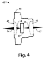
- Fig. 4 is a cross-sectional schematic view illustrating the optical subassembly of Fig. 1.
- the optical subassembly for wavelength conversion is particularly useful for converting the output of a short-wavelength vertical-cavity surface-emitting laser (VCSEL) into a long wavelength laser output.
- VCSEL vertical-cavity surface-emitting laser
- the present invention is applicable to both single spatial mode laser output and to multi-mode laser output.
- Fig. 1 is a cross sectional schematic view illustrating an optical assembly 10 constructed in accordance with an aspect of the invention.
- Optical assembly 10 includes optical assembly housing 18 in which TO package 11 and optical subassembly 40 reside.
- Optical assembly housing 18 may be, for example, an optical component that may be soldered, or otherwise assembled to a circuit board, or may be an optical connector to which may be attached a fiber optic connector 12, which connects a fiber optic cable to the optical assembly 10.
- TO package 11 may be a typical TO-46 header package as known in the art.
- TO package 11 may be any standard package containing short wavelength laser 20.
- short-wavelength laser 20 may not necessarily be packaged in a TO package and may be mounted directly into the optical assembly 10.
- short wavelength laser 20 is preferably a VCSEL.
- Short wavelength laser 20 may be independently optimized, assembled, tested and packaged into TO package 11. The optimization of the short-wavelength laser includes maximizing the wallplug efficiency and adjusting the beam divergence to optimize coupling to the long-wavelength laser.
- the wallplug efficiency is defined as the ratio of optical output power to electrical input power to the device.
- electrical connection 19 short-wavelength laser 20 is electrically pumped, or driven by an appropriate laser driver.
- Optical assembly housing 18 also includes optical subassembly 40.
- Optical subassembly 40 includes long-wavelength laser 30, which may be a vertical-cavity surface-emitting laser.
- Short-wavelength laser 20 preferably emits light at a wavelength of approximately 850 to 1200 nm
- long-wavelength laser 30 preferably emits light at a wavelength of approximately 1300 nm to 1550 nm.
- the conversion efficiency between the short wavelength laser 20 and the long wavelength laser 40 can be improved if the short wavelength laser 20 can be located as close to the long wavelength laser 40 as possible without interfering with the optimization of the long wavelength laser 40. Locating the short wavelength laser 20 close to the long wavelength laser 40 improves the transfer of photon energy between the two lasers.
- the long-wavelength laser 30 may be independently optimized, assembled, tested and installed within optical subassembly 40.
- the long-wavelength laser optimization may include maximizing the absorption of the short wavelength light originating from the short-wavelength laser, minimizing the threshold power, maximizing the output efficiency, and adjusting the cavity for either single or multiple transverse mode operation.
- Optical subassembly 40 is modular in that it may be inserted into optical assembly housing 18 and easily removed. For example, optical subassembly 40 may be snapped into place. Alternatively, optical subassembly may be permanently affixed within optical assembly housing 18.
- Long wavelength laser 30 is electrically passive, meaning that no electrical pumping is necessary. Short wavelength laser 20 optically pumps long wavelength laser 30. Consequently, long wavelength laser 30 requires no electrical connections.
- TO package 11 can be installed within optical housing 18.
- long wavelength laser 30 can be independently optimized and installed in optical subassembly 40.
- Optical subassembly 40 may be installed within optical assembly housing 18 thus completing optical assembly 10.
- short wavelength laser 20 emits short wavelength laser output 14, which is directed toward optical subassembly 40.
- Optical subassembly 40 optionally includes a plurality of optical elements, to be described in detail with reference to Fig. 2. If included, at least one of the optional optical elements focuses the short wavelength laser output 14 onto long wavelength laser 30. Another optical element focuses the long wavelength output 17 of long wavelength laser 30 into fiber optic connector 12.
- optical subassembly 40 When installed within optical assembly housing 18, optical subassembly 40 should be aligned with TO package 11 such that the short wavelength laser output 14 is optimally focused onto optical subassembly 40, and thus long wavelength laser 30, such that the spot size of short wavelength laser output 14 produces maximum efficiency in the long-wavelength output.
- the short wavelength laser spot size is optimally chosen to yield a single mode output for the long wavelength laser.
- the alignment and focus between the short wavelength laser 20 and the long wavelength laser 30 can be realized by specially designed mechanical guides or any manner in which the optical subassembly 40 can be precisely located within the optical assembly housing 18 and with respect to the short wavelength laser 20.
- the optical subassembly 40 is colinearly located in the optical assembly housing 18.
- Optional optics can improve the ability to focus the short wavelength output 14 onto the optical subassembly 40, which contains the long wavelength laser 30.
- the optical subassembly 40 is mounted such that the short wavelength laser output 14 is focused to a desired spot size on the long wavelength laser 30.
- the optical subassembly 40 can be glued, soldered or mechanically held in place using, for example, a retainer ring, in the optical assembly housing 18. Alternatively, the optical subassembly 40 can be removably mounted within the optical assembly housing 18.
- the short wavelength laser output 14 is absorbed by the long wavelength laser 30, which causes the long wavelength laser to generate electron-hole pairs in the absorbing layers in the long wavelength laser 30.
- the electron-hole pairs are funnelled into the active region of the long wavelength laser 30 where these electron-hole pairs recombine emitting light at the longer wavelength as long wavelength laser output 17.
- Long wavelength laser output 17 is preferably of a single longitudinal mode and a single spatial mode for optical communications, resulting in a single frequency output that may be efficiently focused into an optical fiber.
- the long wavelength laser output may be multi-mode for other applications.
- Short wavelength laser 20 generally includes a first mirror 24 located upon a substrate 22, an active layer 26, a second mirror 27, and electrical contacts 21 and 28.
- the two mirrors 24 and 27, as known in the art, may be comprised of multiple layers of aluminum-gallium arsenide (AlGaAs) alloy with alternating composition values in order to produce a structure with layers of alternating values of the refractive index.
- AlGaAs aluminum-gallium arsenide
- the composition of the alloy varies from layer to layer in such a way that the refractive index of the layers varies from high to low, and vice versa.
- Such layered mirrors 24 and 27 are sometimes referred to as Bragg mirrors, or distributed Brag reflectors (DBRs).
- the ratio between the refractive indexes of the high-index and the low index-layer together with the number of layers determines the reflectivity of the mirror.
- the thickness of each low-index and high-index layer in such a mirror is ⁇ /4n (or odd multiples thereof), where ⁇ is the in-vacuum wavelength of light that the laser is designed to emit, and n is the refractive index of the material. Note that any odd integer multiple of ⁇ /4n may be used. For example, material thickness of 3 ⁇ /4n or 5 ⁇ /4n may also be used.
- Typical material choice for the short wavelength VCSEL 20 shown in Fig.2 is aluminum-gallium arsenide with two different compositions because the refractive index varies with the aluminum composition.
- DBR 24 has maximum high reflectivity (approaching 99.9%) because light will be emitted opposite from the substrate 22.
- Active layer 26 is grown over the DBR 24.
- Active layer 26 comprises alternating layers of gallium arsenide (GaAs), aluminum-gallium arsenide (AlGaAs), indium-gallium arsenide (InGaAs) or aluminum-indium-gallium arsenide (AlInGaAs), for example, forming multiple quantum wells.
- GaAs gallium arsenide
- AlGaAs aluminum-gallium arsenide
- InGaAs indium-gallium arsenide
- AlInGaAs aluminum-indium-gallium arsenide
- the output DBR 27 is grown over the active layer 26. While also comprising multiple layers of aluminum-gallium arsenide, DBR 27 has a smaller number of layers to provide a typically lower reflectivity required of the output mirror. The reflectivity of DBR 27 is optimized for maximum laser speed and efficiency.
- Light output 14 indicates the light output of short wavelength laser 20.
- DBR 27 is more transmissive than DBR 24 for the reason that light will be emitted through DBR 27 in the direction indicated by light output 14.
- the DBR mirrors 24 and 27 are designed and doped accordingly to present a low resistance, thus enabling current to flow to the active region 26 as known to those having ordinary skill in the art.
- Electrode 21 is applied to substrate 22 and electrode 28 is applied to active region 26. Current flowing between electrode 21 and electrode 28 electrically pumps active region 26 resulting in the desired short wavelength output 14. It should be noted that only the major portions of short wavelength laser 20 have been described and that the description above is merely one technique for developing a short wavelength laser. Many other techniques may be employed, which remain within the scope of the invention.
- Fig. 3 is a simplified cross-sectional view illustrating the long wavelength laser 30 of Fig. 1.
- Long wavelength laser 30 includes two mirrors 34 and 37 between which is located active layer 36.
- the two mirrors of the long-wavelength laser 30 are comprised of multiple layers with alternating refractive index values, similar in construction to the mirrors 24 and 27 of the short-wavelength VCSEL 20.
- the laser cavity, formed by the two mirrors 34 and 37 and the active layer 36, of laser 30 are tuned to a longer wavelength, in the range of 1300 nm to 1600 nm.
- the material choices for the mirrors 34 and 37 include semiconductors, such as, aluminum-indium-gallium arsenide alloys (AlInGaAs), aluminum-gallium arsenide antimonide alloys (AlGaAsSb) or indium-gallium arsenide phosphide (InGaAsP) alloys, which are latticed matched to indium phosphide (InP). Because no electrical current passes through mirrors 34 and 37, they can be made of unintentionally doped semiconducting layers. Typically a gas having the desired dopant (such as zinc or silicon) is introduced with the other gases needed to grow the semiconductor.
- AlInGaAs aluminum-indium-gallium arsenide alloys
- AlGaAsSb aluminum-gallium arsenide antimonide alloys
- InGaAsP indium-gallium arsenide phosphide
- a gas having the desired dopant such as zinc or
- Unintentional doping means that no dopant species are introduced during the growth of the semiconductor.
- An unintentionally doped semiconductor will exhibit high resistance and lower free carrier absorption. This allows for very low loss mirrors since absorption due to free-carrier absorption (introduced by doping the semiconductors) has been eliminated.
- DBR 37 may also be realized using amorphous dielectric combinations, such as silicon dioxide, titanium dioxide, tantalum pentoxide and similar materials. If amorphous dielectrics are used, due to their larger refractive index ratio between the high-index and low-index materials, the mirrors will typically require fewer layers than the semiconductor alloy combinations to achieve comparable reflectivity.
- Active layer 36 is grown over DBR 34.
- Active layer 36 comprises, for example, alternating layers of indium gallium-arsenide phosphide (InGaAsP) and indium phosphide (InP) or aluminum-indium-gallium arsenide (AlInGaAs forming multiple quantum wells.
- the material choice and its composition may vary depending on the desired wavelength output of the device.
- Other choices of suitable active layers which are lattice matched to gallium arsenide substrates (GaAs), such as indium-gallium-arsenide nitrides (InGaAsN) and gallium-arsenide-antimonide alloys (GaAsSb), may also be used.
- Active layers grown on GaAs may use the higher reflectivity mirrors obtainable using the aluminum-gallium arsenide (AlGaAs) alloys due to their higher index contrast.
- DBR 37 is grown over active layer 36.
- DBR 37 is similar in structure to DBR 34.
- the light output 17 indicates the light output of long-wavelength laser 30.
- DBR 37 is less reflective than DBR 34 because light will be emitted through DBR 37 in the direction indicated by light output 17.
- Other means of creating the long wavelength cavity may also be implemented such as wafer bonding the active layer 36 to either semiconductor or dielectric mirrors; or etching holes in the substrate and depositing dielectric DBR mirrors on both sides of the active region to form the optical cavity.
- Long-wavelength laser 30 is optically pumped by short wavelength light 14 that emanates from the short-wavelength laser 20, and emits long wavelength light output 17.
- the long-wavelength laser cavity is designed to absorb short-wavelength light 14 incident upon it, and emit long-wavelength light 17. This is done by designing the active layer 36 to efficiently absorb short-wavelength light and by designing the mirror 34 to transmit the short-wavelength light 14 into the long-wavelength cavity to be absorbed by the active layer 36.
- the output mirror 37 may, but need not, be designed to reflect the short-wavelength light back into the cavity to be further absorbed in the active layer 36, and also to prevent short wavelength emission through to the long-wavelength output 17.
- the two mirrors 34 and 37 should be highly reflective for long-wavelength light to provide low threshold and high efficiency for long-wavelength emission.
- the orientation of the long-wavelength laser regarding which side is pumped and which side emits the long-wavelength light is arbitrary. Namely, the long-wavelength laser may be pumped from the substrate side, as shown in Fig. 3, or from the opposite side. Similarly the long-wavelength light output may be taken out from either side as well. It will be clear to persons skilled in the art that these variations are within the scope of the invention.
- Fig. 4 is a cross-sectional schematic view illustrating the optical subassembly 40 of Fig. 1.
- Optical subassembly 40 includes optical subassembly housing 48 in which long wavelength laser 30 is housed.
- Long wavelength laser 30 may, but need not, include a heat-sinking metallization pattern on its surface to aid in the dissipating of the heat generated through the absorption of short wavelength laser output 14.
- the long wavelength laser 30 is fixed within housing 48 by a thermally conducting adhesive or may include metallized contacts, which can be used to solder the long wavelength laser 30 to the housing 48. This allows the heat generated in the long wavelength laser 30 to be extracted through the housing 48.
- optical subassembly 40 optionally includes first optical element 41 and second optical element 42.
- First optical element 41 focuses the short wavelength laser output 14 from short wavelength laser 20 (Fig. 1) onto long wavelength laser 30 as illustrated.
- the short wavelength laser light 14 is focused onto long wavelength laser 30 with a spot size optimized for lowest threshold power and highest output efficiency of the long-wavelength laser 30.
- the presence of the optical elements 41 and 42 in the assembly is optional and may be used to improve the mutual coupling of light between the short wavelength laser 20, the long wavelength laser 30, and the optical fiber into which the long-wavelength light 17 will ultimately be focused.
- the short wavelength laser light 14 is absorbed by long wavelength laser 30, which generates electron-hole pairs. These electron-hole pairs recombine to generate light at the longer wavelength, at which the cavity of the long wavelength laser 30 has maximum gain.
- This light is emitted from long wavelength laser 40 as long wavelength laser light 17 towards second optical element 42, if present.
- Second optical element 42 helps focus the long wavelength laser light 17 and aids in minimizing the spot size of the long wavelength light output 17.
- Long wavelength light output 17 may now be focused into, for example, an optical fiber connector 12 (Fig. 1) to which is connected an optical fiber for transmission over a fiber optics communications system.
- optical subassembly 40 within optical assembly housing 18 in optical communication with short wavelength laser 20 allows each laser device to be independently optimized, packaged and tested, and most importantly, used for independent purposes. If short wavelength output is desired then only the short wavelength assembly 20 is used. If a long wavelength output is desired, then the optical subassembly 40 is combined within the optical assembly 10 to provide a long wavelength light output.
- the long-wavelength optical subassembly 30 may be manufactured as an independent optical element which may be inserted into the laser assembly 10 in such a way that it is positioned in the light output path of the short-wavelength laser 20.
- the long-wavelength output 17 of long wavelength laser 30 couples into the fiber, which is brought into proximity by the help of a connector guide as known to those skilled in the art.
- the short-wavelength laser output optically pumps the long-wavelength laser, which then emits light into the fiber.
Landscapes
- Physics & Mathematics (AREA)
- Condensed Matter Physics & Semiconductors (AREA)
- General Physics & Mathematics (AREA)
- Electromagnetism (AREA)
- Optics & Photonics (AREA)
- Semiconductor Lasers (AREA)
Abstract
Description
Claims (10)
- An optical assembly (10), comprising:a housing (18);a prefabricated short wavelength laser (20) located in the housing (18) and optimized for a short wavelength laser output (14);a prefabricated long wavelength laser (30) optimized for a long wavelength laser output (17); andan optical subassembly (40) structured to accommodate the prefabricated long wavelength laser (30) and located within the housing (18) in a position at which the output (14) of the short wavelength laser (20) is applied to the long wavelength laser (30).
- The optical assembly (10) of claim 1, wherein the optical subassembly (40) is removably mounted in the housing (18).
- The optical assembly (10) of claim 1 or 2, wherein the short wavelength laser (20) optically pumps the long wavelength laser (30) to produce a long wavelength laser output (17).
- The optical assembly (10) of one of the preceding claims, wherein the short wavelength laser output (14) is excluded from the long wavelength laser output (17)
- The optical assembly (10) of one of the preceding claims, wherein the housing (18) is structured to locate the optical subassembly (40) and the prefabricated short wavelength laser (20) in a predetermined position.
- A method for forming an optical assembly (10), comprising the steps of:locating a prefabricated short wavelength laser (20) in a housing (18);locating a long wavelength laser (30) in an optical subassembly (40); andplacing the optical subassembly (40) containing the long wavelength laser (30) in the housing (18) and in a light output path of the short wavelength laser (20), such that an output (14) of the short wavelength laser (20) is directed into the optical subassembly (40) and optically pumps the long wavelength laser (30) resulting in a long wavelength laser output (17).
- The method of claim 6, wherein the long wavelength laser output (17) excludes the short wavelength laser output (14).
- The method of claim 6 or 7, wherein the optical subassembly (40) is removably mounted in the housing (18).
- The method of one of claims 6 - 8, further comprising the step of including a first optical element (41) in the optical subassembly (40), the first optical element (41) located in the light output path of the short wavelength laser (20).
- The method of claim 9, further comprising the step of focusing the output (14) of the short wavelength laser (20) through the optical element (41) in order to form an input to the long wavelength laser (30).
Applications Claiming Priority (2)
| Application Number | Priority Date | Filing Date | Title |
|---|---|---|---|
| US703389 | 2000-10-31 | ||
| US09/703,389 US6553051B1 (en) | 2000-10-31 | 2000-10-31 | System for optically pumping a long wavelength laser using a short wavelength laser |
Publications (3)
| Publication Number | Publication Date |
|---|---|
| EP1211764A2 true EP1211764A2 (en) | 2002-06-05 |
| EP1211764A3 EP1211764A3 (en) | 2003-05-14 |
| EP1211764B1 EP1211764B1 (en) | 2005-08-31 |
Family
ID=24825179
Family Applications (1)
| Application Number | Title | Priority Date | Filing Date |
|---|---|---|---|
| EP01114657A Expired - Lifetime EP1211764B1 (en) | 2000-10-31 | 2001-06-19 | System for optically pumping a long wavelength laser using a short wavelength laser |
Country Status (4)
| Country | Link |
|---|---|
| US (1) | US6553051B1 (en) |
| EP (1) | EP1211764B1 (en) |
| JP (1) | JP4246942B2 (en) |
| DE (1) | DE60113041T2 (en) |
Cited By (2)
| Publication number | Priority date | Publication date | Assignee | Title |
|---|---|---|---|---|
| EP1643603A1 (en) * | 2004-09-29 | 2006-04-05 | Wavelight Laser Technologie AG | Lasersystem with solid state laser heads |
| EP1848073A1 (en) * | 2006-04-19 | 2007-10-24 | Multitel ASBL | Switchable laser device and method for operating said device |
Families Citing this family (7)
| Publication number | Priority date | Publication date | Assignee | Title |
|---|---|---|---|---|
| AU2001286614A1 (en) * | 2000-08-22 | 2002-03-04 | The Regents Of The University Of California | A method for aperturing vertical-cavity surface-emitting lasers (vscels) |
| US6845114B2 (en) * | 2002-10-16 | 2005-01-18 | Eastman Kodak Company | Organic laser that is attachable to an external pump beam light source |
| TW595013B (en) * | 2002-11-04 | 2004-06-21 | Arima Optoelectronics Corp | Semiconductor laser using asymmetric quantum well structure |
| US7433381B2 (en) * | 2003-06-25 | 2008-10-07 | Finisar Corporation | InP based long wavelength VCSEL |
| CN101652711A (en) * | 2007-03-30 | 2010-02-17 | 柯尼卡美能达精密光学株式会社 | Second harmonic light generating device and manufacturing method thereof |
| US9124062B2 (en) | 2012-03-22 | 2015-09-01 | Palo Alto Research Center Incorporated | Optically pumped surface emitting lasers incorporating high reflectivity/bandwidth limited reflector |
| JP2014093437A (en) * | 2012-11-05 | 2014-05-19 | Ricoh Co Ltd | Laser pumped laser device and process of manufacturing the same |
Family Cites Families (10)
| Publication number | Priority date | Publication date | Assignee | Title |
|---|---|---|---|---|
| US4462103A (en) | 1982-03-23 | 1984-07-24 | The United States Of America As Represented By The Secretary Of The Air Force | Tunable CW semiconductor platelet laser |
| US4731795A (en) * | 1986-06-26 | 1988-03-15 | Amoco Corporation | Solid state laser |
| US4947402A (en) | 1988-04-25 | 1990-08-07 | Lightwave Electronics Corporation | Two-mirror shaping of a non-circular optical pumping beam and lasers using same |
| DE3925201A1 (en) * | 1989-07-29 | 1991-02-07 | Messerschmitt Boelkow Blohm | OPTICAL BENCH FOR MOUNTING OPTICAL, ELECTRICAL AND OTHERS COMPONENTS |
| JP3265173B2 (en) * | 1995-01-10 | 2002-03-11 | 三菱電機株式会社 | Solid state laser device |
| US5513204A (en) | 1995-04-12 | 1996-04-30 | Optical Concepts, Inc. | Long wavelength, vertical cavity surface emitting laser with vertically integrated optical pump |
| DE19523267A1 (en) * | 1995-06-27 | 1997-01-02 | Bosch Gmbh Robert | Vertical cavity surface emitting laser module for transmitter in long wavelength region |
| US5754578A (en) | 1996-06-24 | 1998-05-19 | W. L. Gore & Associates, Inc. | 1250-1650 nm vertical cavity surface emitting laser pumped by a 700-1050 nm vertical cavity surface emitting laser |
| CA2242670A1 (en) * | 1997-07-14 | 1999-01-14 | Mitel Semiconductor Ab | Field modulated vertical cavity surface-emitting laser with internal optical pumping |
| US6289031B1 (en) * | 1999-05-14 | 2001-09-11 | Raytheon Company | Integrated lightweight optical bench and miniaturized laser transmitter using same |
-
2000
- 2000-10-31 US US09/703,389 patent/US6553051B1/en not_active Expired - Lifetime
-
2001
- 2001-06-19 EP EP01114657A patent/EP1211764B1/en not_active Expired - Lifetime
- 2001-06-19 DE DE60113041T patent/DE60113041T2/en not_active Expired - Lifetime
- 2001-10-30 JP JP2001332027A patent/JP4246942B2/en not_active Expired - Fee Related
Cited By (4)
| Publication number | Priority date | Publication date | Assignee | Title |
|---|---|---|---|---|
| EP1643603A1 (en) * | 2004-09-29 | 2006-04-05 | Wavelight Laser Technologie AG | Lasersystem with solid state laser heads |
| WO2006034783A1 (en) * | 2004-09-29 | 2006-04-06 | Wavelight Laser Technologie Ag | Laser system with solid laser heads |
| EP1848073A1 (en) * | 2006-04-19 | 2007-10-24 | Multitel ASBL | Switchable laser device and method for operating said device |
| EP1848074A1 (en) * | 2006-04-19 | 2007-10-24 | Multitel ASBL | Switchable laser device and method for operating the same |
Also Published As
| Publication number | Publication date |
|---|---|
| EP1211764A3 (en) | 2003-05-14 |
| JP4246942B2 (en) | 2009-04-02 |
| DE60113041T2 (en) | 2006-05-18 |
| DE60113041D1 (en) | 2005-10-06 |
| EP1211764B1 (en) | 2005-08-31 |
| JP2002151783A (en) | 2002-05-24 |
| US6553051B1 (en) | 2003-04-22 |
Similar Documents
| Publication | Publication Date | Title |
|---|---|---|
| US5978401A (en) | Monolithic vertical cavity surface emitting laser and resonant cavity photodetector transceiver | |
| KR100229051B1 (en) | Long wavelength vertical cavity surface emitting laser with vertically integrated optical pump | |
| US6252896B1 (en) | Long-Wavelength VCSEL using buried bragg reflectors | |
| US5812571A (en) | High-power vertical cavity surface emitting laser cluster | |
| US7288421B2 (en) | Method for forming an optoelectronic device having an isolation layer | |
| RU2623663C2 (en) | Surface-emitting laser device with vertical external resonator with optical pumping | |
| EP1309051A1 (en) | Resonant reflector for improved optoelectronic device performance and enhanced applicability | |
| JP2004503118A (en) | VCSEL and VCSEL array with integrated microlenses for use in semiconductor laser pumped solid-state laser systems | |
| EP1461850A1 (en) | Integral vertical cavity surface emitting laser and power monitor | |
| EP3557706B1 (en) | Communication system employing surface-coupled optical devices | |
| US6845118B1 (en) | Encapsulated optoelectronic devices with controlled properties | |
| US6553051B1 (en) | System for optically pumping a long wavelength laser using a short wavelength laser | |
| JP2967057B2 (en) | Surface type optical multifunctional element | |
| US6963061B2 (en) | Orthogonal coupled transceiver | |
| US11949211B2 (en) | Broadband active mirror architecture for high power optically pumped semiconductor disk lasers | |
| CA2366583C (en) | Encapsulated optoelectronic devices with controlled properties | |
| US7339971B2 (en) | Optical element and optical module | |
| JP2002252418A (en) | Optical communication system | |
| Warren et al. | Integration of diffractive lenses with addressable vertical-cavity laser arrays | |
| EP1163711A1 (en) | Encapsulated optoelectronic devices with controlled properties | |
| WO2026071166A1 (en) | Vertical cavity surface emitting laser device system and vertical cavity surface emitting laser device array | |
| Demaria | Layer Design of Highly Efficient Optically Pumped Semiconductor Disk Lasers | |
| Halbritter et al. | Properties of micromechanically tunable VCSELs |
Legal Events
| Date | Code | Title | Description |
|---|---|---|---|
| PUAI | Public reference made under article 153(3) epc to a published international application that has entered the european phase |
Free format text: ORIGINAL CODE: 0009012 |
|
| AK | Designated contracting states |
Kind code of ref document: A2 Designated state(s): AT BE CH CY DE DK ES FI FR GB GR IE IT LI LU MC NL PT SE TR |
|
| AX | Request for extension of the european patent |
Free format text: AL;LT;LV;MK;RO;SI |
|
| PUAL | Search report despatched |
Free format text: ORIGINAL CODE: 0009013 |
|
| AK | Designated contracting states |
Designated state(s): AT BE CH CY DE DK ES FI FR GB GR IE IT LI LU MC NL PT SE TR |
|
| AX | Request for extension of the european patent |
Extension state: AL LT LV MK RO SI |
|
| 17P | Request for examination filed |
Effective date: 20031015 |
|
| AKX | Designation fees paid |
Designated state(s): DE FR GB |
|
| 17Q | First examination report despatched |
Effective date: 20040128 |
|
| GRAP | Despatch of communication of intention to grant a patent |
Free format text: ORIGINAL CODE: EPIDOSNIGR1 |
|
| GRAS | Grant fee paid |
Free format text: ORIGINAL CODE: EPIDOSNIGR3 |
|
| GRAA | (expected) grant |
Free format text: ORIGINAL CODE: 0009210 |
|
| AK | Designated contracting states |
Kind code of ref document: B1 Designated state(s): DE FR GB |
|
| REG | Reference to a national code |
Ref country code: GB Ref legal event code: FG4D |
|
| REF | Corresponds to: |
Ref document number: 60113041 Country of ref document: DE Date of ref document: 20051006 Kind code of ref document: P |
|
| ET | Fr: translation filed | ||
| PGFP | Annual fee paid to national office [announced via postgrant information from national office to epo] |
Ref country code: FR Payment date: 20060620 Year of fee payment: 6 |
|
| PGFP | Annual fee paid to national office [announced via postgrant information from national office to epo] |
Ref country code: GB Payment date: 20060626 Year of fee payment: 6 |
|
| PLBE | No opposition filed within time limit |
Free format text: ORIGINAL CODE: 0009261 |
|
| STAA | Information on the status of an ep patent application or granted ep patent |
Free format text: STATUS: NO OPPOSITION FILED WITHIN TIME LIMIT |
|
| REG | Reference to a national code |
Ref country code: GB Ref legal event code: 732E |
|
| 26N | No opposition filed |
Effective date: 20060601 |
|
| GBPC | Gb: european patent ceased through non-payment of renewal fee |
Effective date: 20070619 |
|
| REG | Reference to a national code |
Ref country code: FR Ref legal event code: ST Effective date: 20080229 |
|
| PG25 | Lapsed in a contracting state [announced via postgrant information from national office to epo] |
Ref country code: GB Free format text: LAPSE BECAUSE OF NON-PAYMENT OF DUE FEES Effective date: 20070619 |
|
| PG25 | Lapsed in a contracting state [announced via postgrant information from national office to epo] |
Ref country code: FR Free format text: LAPSE BECAUSE OF NON-PAYMENT OF DUE FEES Effective date: 20070702 |
|
| REG | Reference to a national code |
Ref country code: DE Ref legal event code: R082 Ref document number: 60113041 Country of ref document: DE Representative=s name: DILG HAEUSLER SCHINDELMANN PATENTANWALTSGESELL, DE |
|
| REG | Reference to a national code |
Ref country code: DE Ref legal event code: R081 Ref document number: 60113041 Country of ref document: DE Owner name: AVAGO TECHNOLOGIES GENERAL IP (SINGAPORE) PTE., SG Free format text: FORMER OWNER: AVAGO TECHNOLOGIES FIBER IP (SINGAPORE) PTE. LTD., SINGAPORE, SG Effective date: 20130628 Ref country code: DE Ref legal event code: R082 Ref document number: 60113041 Country of ref document: DE Representative=s name: DILG HAEUSLER SCHINDELMANN PATENTANWALTSGESELL, DE Effective date: 20130628 |
|
| REG | Reference to a national code |
Ref country code: DE Ref legal event code: R082 Ref document number: 60113041 Country of ref document: DE Representative=s name: DILG, HAEUSLER, SCHINDELMANN PATENTANWALTSGESE, DE Ref country code: DE Ref legal event code: R081 Ref document number: 60113041 Country of ref document: DE Owner name: BROADCOM INTERNATIONAL PTE. LTD., SG Free format text: FORMER OWNER: AVAGO TECHNOLOGIES GENERAL IP (SINGAPORE) PTE. LTD., SINGAPORE, SG Ref country code: DE Ref legal event code: R082 Ref document number: 60113041 Country of ref document: DE Representative=s name: DILG HAEUSLER SCHINDELMANN PATENTANWALTSGESELL, DE Ref country code: DE Ref legal event code: R081 Ref document number: 60113041 Country of ref document: DE Owner name: AVAGO TECHNOLOGIES INTERNATIONAL SALES PTE. LT, SG Free format text: FORMER OWNER: AVAGO TECHNOLOGIES GENERAL IP (SINGAPORE) PTE. LTD., SINGAPORE, SG |
|
| PGFP | Annual fee paid to national office [announced via postgrant information from national office to epo] |
Ref country code: DE Payment date: 20190627 Year of fee payment: 19 |
|
| REG | Reference to a national code |
Ref country code: DE Ref legal event code: R082 Ref document number: 60113041 Country of ref document: DE Representative=s name: DILG, HAEUSLER, SCHINDELMANN PATENTANWALTSGESE, DE Ref country code: DE Ref legal event code: R081 Ref document number: 60113041 Country of ref document: DE Owner name: BROADCOM INTERNATIONAL PTE. LTD., SG Free format text: FORMER OWNER: AVAGO TECHNOLOGIES INTERNATIONAL SALES PTE. LTD., SINGAPUR, SG |
|
| REG | Reference to a national code |
Ref country code: DE Ref legal event code: R119 Ref document number: 60113041 Country of ref document: DE |
|
| PG25 | Lapsed in a contracting state [announced via postgrant information from national office to epo] |
Ref country code: DE Free format text: LAPSE BECAUSE OF NON-PAYMENT OF DUE FEES Effective date: 20210101 |