TECHNICAL FIELD
The present invention relates to a film forming
method using magnetron sputtering, a magnetron type
sputtering apparatus used to form a film such as a
titanium nitride film or the like, and a magnetron unit
used for the sputtering apparatus.
BACKGROUND ART
The sputtering method is known as one film
formation technique in semiconductor manufacturing
processes. The sputtering method refers to a method in
which film formation is accomplished by bombarding the
surface of a target constituting a cathode with
positive ions of a treatment gas, ordinarily argon ions,
in a plasma, and depositing target particles (hereafter
referred to as "sputtered particles") that are
sputtered from this surface on a semiconductor wafer on
the anode side.
Furthermore, such sputtering methods include a
method known as the reactive sputtering method, which
is used to form thin films of compounds such as TiN
films. This reactive sputtering method is a method in
which a thin film of such a compound is formed by
introducing an inert gas (e. g., nitrogen gas) into the
chamber in addition to argon gas, ionizing this inert
gas by means of a plasma, and reacting [this ionized
gas] with the sputtered particles (e. g., titanium) on
the surface of the wafer.
In a film forming apparatus which utilizes such
a sputtering method, i. e., a sputtering apparatus, a
so-called magnetron system (magnetron sputtering) is
widely employed in order to improve the sputtering
efficiency by increasing the plasma density in the
vicinity of the surface of the target. In this system,
a magnetron unit which has a plurality of magnet units
is disposed on the back surface side of the target, and
a magnetic field is generated in the vicinity of the
target inside the vacuum chamber. Since those lines of
magnetic force in this magnetic field that intersect
the electric field between the target and the wafer
confine the electrons from the target into a region
located in the vicinity of the target, the plasma
density in this region is increased.
A conventional magnetron unit comprises a
circular base plate which is disposed parallel to and
coaxially with the target on the back surface side of
the target, and magnet units which are fastened to the
undersurface of this base plate. The base plate is
connected to a driving source that rotationally drives
the base plate, so that the magnetic field formed by
the magnet units moves in the circumferential direction.
In cases where sputtering is performed using a
magnetron type sputtering apparatus, the internal
stress of the resulted thin film may be a strong
compressive stress. In particular, it has been
confirmed that the internal stress reaches considerable
levels in the case of remote (long throw) sputtering.
Here, the term "remote sputtering method" refers
to a method in which the distance between the target
and the semiconductor wafer is longer than in a
conventional standard sputtering apparatus. In this
method, sputtered particles that advance at a large
angle relative to the semiconductor wafer reach regions
outside the wafer, and only sputtered particles that
advance in more or less the perpendicular direction are
deposited on the wafer. Accordingly, in this method,
overhang in hole entrance parts can be prevented, so
that finer wiring patterns can be handled.
If the internal stress of the thin film exceeds
a standard value (this standard value fluctuates in
processes preceding and following the process in
question), fine cracks might be generated in the thin
film as a result of warping of the semiconductor wafer;
consequently, there is a danger that problems will
occur in the focusing of the subsequent exposure
process or the like.
With the foregoing in view, it is an object of
the present invention to provide means for reducing the
internal stress of thin films formed by the sputtering
method.
DISCLOSURE OF THE INVENTION
The present inventors conducted various
investigations in order to achieve the abovementioned
object; as a result, the inventors discovered that the
magnetic field formed by the magnetron unit has an
effect on the internal stress of the thin film. To
describe this in greater detail, in cases where the
component of the lines of magnetic force in the
magnetic field formed by the magnetron unit that is
oriented toward the semiconductor wafer is greater than
the component that is parallel to the target, the
electrons in the plasma are drawn out toward the
semiconductor wafer, so that a self-bias is generated
at the surface of the wafer. As a result, it appears
that the positive ions in the plasma bombard the film
on the semiconductor wafer, so that the compressive
internal stress in the film increases. Especially in
the case of remote sputtering, since the distance to
the semiconductor wafer is long, the ions directed
toward the semiconductor wafer are accelerated and have
a high kinetic energy; as a result, the compressive
internal stress is further increased.
Accordingly, the film forming method using
magnetron sputtering in accordance with the present
invention is a film forming method in which a
sputtering target and a substrate to be treated facing
this sputtering target are placed inside a chamber, a
process gas is introduced into the chamber, and a film
is formed on the surface of the substrate by generating
a plasma on the erosion surface of the sputtering
target by means of a magnetron unit, this method being
characterized in that sputtering is performed in a
state in which the component of the lines of magnetic
force of the magnetic field formed by the magnetron
unit that leaves this magnetron unit and is directed
toward the substrate is reduced compared to the
component that leaves the magnetron unit and then again
returns to the magnetron unit.
As a result of the use of such a method, there
is a decrease in the lines of magnetic force that are
directed toward the substrate being treated from the
sputtering target, so that the self-bias on the
substrate being treated can be suppressed to a low
value or to zero. Accordingly, the effect of ion
bombardment on the substrate being treated can be
reduced, so that an increase in internal stress can be
prevented.
Furthermore, in the abovementioned film forming
method, the sputtering target is constructed so that
this target contains at least titanium, and the process
gas contains at least nitrogen; accordingly, this
method is especially effective for forming a titanium
nitride film on the surface of the substrate.
In this way, a titanium nitride film can be
formed on the surface of the substrate, and the
compressive internal stress in the titanium nitride
film thus formed can be reduced.
Furthermore, another aspect of the present
invention is directed to the magnetron unit, and this
magnetron unit is a magnetron unit formed by attaching
a plurality of magnet units for forming a magnetic
field in the vacuum chamber of the sputtering apparatus
to a base plate, which is characterized in that a
construction is used in which the lines of magnetic
force between adjacent magnet units are in equilibrium.
Furthermore, a state in which the component of
the lines of magnetic force of the magnetic field
formed by the magnetron unit that leaves this magnetron
unit and is directed toward the substrate is
sufficiently smaller than the component that leaves the
magnetron unit and then again returns to this magnetron
unit is referred to as an "equilibrium".
In such a construction, there is a decrease in
the lines of magnetic force that are directed toward
the substrate to be treated (i. e., the semiconductor
wafer) from the target of the sputtering apparatus, so
that the self-bias on the substrate being treated can
be suppressed to a low value or to zero. Accordingly,
the effect of ion bombardment on the substrate can be
reduced, so that an increase in internal stress can be
prevented.
In the abovementioned magnetron unit, the magnet
units are attached on the base plate, and have two
magnetic pole ends of different polarity that are
oriented in the same direction, and that are disposed
with a predetermined gap between these magnetic pole
ends. A construction can be used in which the magnet
units are attached to the base plate in a state in
which the respective magnetic pole ends are oriented in
the opposite direction from the base plate.
With this arrangement of the magnet units, it is
possible to handle the respective magnet units as an
integral whole, so that handling is easy. Furthermore,
the disposition of the respective magnet units can be
selected in a favorable manner on the base plate.
Furthermore, it is preferable to construct a
first annular array of magnet units in which the magnet
units are disposed such that the magnet units surround
a predetermined point, and such that one magnetic pole
end of each magnet unit faces in the centripetal
direction, while the other magnetic pole end of each
magnet unit faces in the centrifugal direction, and to
construct a second annular array of magnet units in
which the second array is arranged such that one
magnetic pole ends of the magnet units in the second
array face in the centripetal direction, the one
magnetic pole ends being of opposite polarity from the
magnetic pole ends in the magnet units of the first
array that face in the centrifugal direction, while the
other magnetic pole ends of the second array face in
the centrifugal direction.
As a result of first and second arrays of magnet
units thus being constructed, the magnet units
constituting the first array is located on the side
that faces in the centripetal direction, and the magnet
units constituting the second array is located on the
side that faces in the centrifugal direction, so that
the respective magnet units are disposed adjacent to
each other. In this case, since the magnetic
polarities of two magnet units that are adjacent to
each other are different, a closed magnetic circuit is
formed between these magnet units, so that the lines of
magnetic force that are directed toward the substrate
are reduced.
Furthermore, the magnet units can also be
constructed from flat-plate-form yoke members that make
of a ferromagnet, and bar magnets that are fixed on
both ends of these yoke members such that a
substantially U-shaped part is formed.
The leakage of lines of magnetic force to the
back surface side of the yoke members can be
sufficiently reduced by constructing the yoke members
of the magnet units from a ferromagnetic material.
Furthermore, it is preferable to attach the
magnet units on the base plate in a manner that allows
the magnet units to be removed.
As a result of using a construction in which the
magnet units can be removed from the base plate, the
arrangement of the magnet units on the base plate can
easily be altered, and the units themselves can easily
be replaces in cases where (for example) the strength
of the magnetic field is altered.
Furthermore, the present invention is directed
to a sputtering apparatus, and this sputtering
apparatus comprises a vacuum chamber, holding means for
the substrate inside the vacuum chamber, a target
disposed with an erosion surface facing the substrate
that is held by the holding means, pressure reduction
means for reducing the pressure inside the vacuum
chamber, gas supplying means for supplying a process
gas to the interior of the vacuum chamber, plasma
generating means for converting the process gas
supplied to the interior of the vacuum chamber into a
plasma, and a magnetron unit of the abovementioned
construction which is disposed on the opposite side of
the target from the erosion surface.
In this construction of the sputtering apparatus,
it is possible to perform sputtering in a state in
which the component of the lines of magnetic force of
the magnetic field formed by the magnetron unit that
leaves this magnetron unit and is directed toward the
substrate is sufficiently reduced compared to the
component that leaves the magnetron unit and then again
returns to this magnetron unit, i. e., it is possible
to perform sputtering in an equilibrium state.
Accordingly, the self-bias on the substrate being
treated can be suppressed to a low value or to zero,
and as a result of this action, the effect of ion
bombardment on the substrate can be reduced, so that an
increase in internal stress can be prevented.
Furthermore, a sputtering apparatus according
to an aspect of the present invention comprises a
chamber, holding means for holding the substrate to be
treated inside the chamber, a target disposed with an
erosion surface facing the substrate, and a magnetron
unit disposed on the opposite side of the target from
the erosion surface, this sputtering apparatus being
characterized in that the magnetron unit comprises a
base plate; a first magnet having a first polarity, the
first magnet being disposed in an annular configuration
on the base plate which is centered on a point that is
offset from the center of rotation of the base plate; a
second magnet having a second polarity which is
different from the first polarity, the second magnet
being disposed on the base plate such that the second
magnet surrounds the first magnet in an annular
configuration; a third magnet having the first polarity,
the third magnet being disposed on the base plate such
that the third magnet surrounds the second magnet in an
annular configuration; and a fourth magnet having the
second polarity, the fourth magnet being disposed on
the base plate such that the fourth magnet surrounds
the third magnet in an annular configuration.
The first to fourth magnets can be constructed,
for example, by arranging a plurality of rod-shaped
sub-magnets, respectively. Alternatively, the first to
fourth magnets may also include magnets in which the
magnets themselves are formed with an annular shape.
Construction of the magnetron unit in this
manner results in a state in which the first magnets
are disposed closest to the predetermined point, with
the second through fourth magnets being successively
disposed further in the centrifugal direction.
Furthermore, in the case of respective magnets arranged
in this manner, magnets that are adjacent on the
centripetal and centrifugal sides have different
polarities, so that closed magnetic circuits can be
formed between these magnets. Moreover, as a result of
this action, a magnetron unit can be constructed in an
equilibrium state in which the component of the lines
of magnetic force that leaves the magnetron unit and is
directed toward the substrate is sufficiently smaller
than the component of the lines of magnetic force that
leaves the magnetron unit and then again returns to the
magnetron unit.
The above and other features and advantages of
the present invention will become more apparent by
reading the following detailed description to those
skilled in the art, while referring to the attached
drawings.
BRIEF DESCRIPTION OF THE DRAWINGS
Fig. 1 is a schematic explanatory view showing a
preferred embodiment of the present invention;
Fig. 2 shows the magnetron unit in Fig. 1 as
viewed from below;
Fig. 3 is a sectional view along line III-III in
Fig. 2, showing the construction of the magnet units
used in the magnetron unit; and
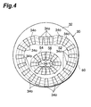
Fig. 4 is a view of another embodiment of the
present invention, showing the magnetron unit as viewed
from below.
BEST MODE FOR CARRYING OUT THE INVENTION
Preferred embodiments of the present invention
will be described in detail below with reference to the
attached figures.
Fig. 1 schematically shows a magnetron type
sputtering apparatus in accordance with the present
invention. The sputtering apparatus 10 in the present
embodiment is used to form a TiN film (titanium nitride
film) on the surface of a semiconductor wafer W which
is a substrate to be treated. This sputtering
apparatus 10 comprises a housing 14 which has a vacuum
chamber 12 formed therein, and a disk-form target 16
which is disposed such that the target closes an upper
opening portion of the housing 14. The target 16 is
constructed from titanium. The housing 14 and the
target 16 are both conductive, and an insulating member
15 is sandwiched between the housing 14 and the target
16. The circular undersurface of the target 16 is
equivalent to an erosion surface whose entire area is
subjected to erosion by sputtering.
A pedestal (holding means) 18 for holding the
semiconductor wafer W on the upper surface thereof is
disposed inside the vacuum chamber 12. The upper
surface of the pedestal 18 is positioned parallel to
and facing the undersurface of the target 16.
Therefore, the wafer W held in a specified position on
the pedestal 18 is parallel to and coaxial with the
undersurface of the target 16. In the shown embodiment,
the dimensions of the target 16 and the gap between the
pedestal 18 and the target 16 are set at values that
are greater than those in a conventional standard
sputtering apparatus, and a remote sputtering method is
applied.
An exhaust port 20 is formed in the housing 14.
A vacuum pump (not shown) such as a cryopump or the
like is connected to this exhaust port 20, and the
pressure inside the vacuum chamber 12 is reduced by
operating this vacuum pump. Specifically, the exhaust
port 20 and vacuum pump constitute pressure reduction
means for reducing the pressure inside the vacuum
chamber 12. Furthermore, a mixed gas including argon
gas and nitrogen gas is supplied to the interior of the
vacuum chamber 12 as a process gas via a port 22 from
gas supplying means (not shown).
The cathode of a direct-current power supply 24
as plasma forming means is connected to the target 16,
and the anode of the direct-current power supply 24 and
the pedestal 18 (i. e., the wafer W) are grounded.
When the mixed gas of argon gas and nitrogen gas is
introduced into the interior of the vacuum chamber 12,
and the direct-current power supply 24 is switched on
so that a voltage is applied between the target 16 and
pedestal 18, a glow discharge is generated so that a
plasma state results. When the argon ions generated by
this discharge strike the undersurface of the target 16,
titanium particles (sputtered particles) or target
atoms are expelled, and these titanium particles are
deposited on the wafer W. Furthermore, the nitrogen
ions in the plasma are directed toward the anode
pedestal 18, and react with the titanium on the wafer W
to form a TiN film.
A magnetron unit 30 for increasing the plasma
density in the vicinity of the target 16 is disposed on
the opposite side of the target 16 from the
undersurface, i. e., above the target 16. As is shown
in Fig. 2, the magnetron unit 30 comprises a circular
base plate 32, and a plurality of magnet units 34 which
are attached on the base plate 32 in a specified
arrangement. The base plate 32 is positioned coaxially
with the target 16 above the target 16, and the
rotating shaft 38 of a driving motor 36 is connected to
the center C of the upper surface of the base plate 32.
Accordingly, when the driving motor 36 is actuated to
rotate the base plate 32, the respective magnet units
34 rotate along the upper surface of the target 16 so
as to prevent the magnetic fields generated by the
respective magnet units from becoming static in one
place.
As seen in Fig. 3, each magnet unit 34 is
constructed from a flat-plate-form yoke member 40 made
of a ferromagnet, and bar magnets 42 and 44 which are
fixed on the end portions of the yoke member 40,
respectively. The two bar magnets 42 and 44 extend in
the same direction. Accordingly, the overall shape of
each magnet unit 34 is substantially U-shaped.
Furthermore, the free end of one bar magnet 42 is an S
pole, while the free end of the other bar magnet 44 is
an N pole. In this embodiment, the areas of the end
surfaces of the respective bar magnets 42 and 44 are
substantially equal. As a result, in the respective
magnet units 34, the lines of magnetic force that
extend between the magnetic pole end surfaces of the
bar magnets 42 and 44 are substantially in equilibrium
(see the broken lines in Fig. 3). Specifically, in
each magnet unit 34, closed magnetic circuit via the
bar magnets 42 and 44 is formed, and the lines of
magnetic force directed to the outside of the magnetic
circuit are considerably reduced. Furthermore, in the
regions of the bar magnets 42 and 44 on the opposite
sides from the end surfaces, the magnetic circuit is
formed through the yoke member 40 of ferromagnet;
accordingly, almost no leakage magnetic flux is
generated.
The magnet units 34 are mounted on the base
plate 32 by appropriate fastening means such as screws
46 with the back surfaces of the yoke members 40
contacting the base plate 32. In such a construction,
the mounting position of the magnet unit 34 can be
freely changed.
In the shown embodiment, the magnet units 34 are
arranged in the double annular arrangement as shown in
Fig. 2. A first array of the magnet units which is
located on the inside surrounds a predetermined point D.
One magnetic pole end (the N pole in Fig. 2) of each
magnet unit 34i (the appended character i indicates the
inside annular array) constituting this first magnet
unit array faces in the centripetal direction (toward
the point D), while the other magnetic pole end (the S
pole in Fig. 2) faces in the centrifugal direction
(away from the point D). Furthermore, the second
magnet unit array which is located on the outside
surrounds the first magnet unit array, and one magnetic
pole end (the N pole in Fig. 2) of each magnet unit 34o
(the appended character o indicates the outside annular
row) constituting this second magnet row faces in the
centripetal direction, while the other magnetic pole
end (the S pole in Fig. 2) faces in the centrifugal
direction. With such an annular arrangement, it is
preferable that the shape of the magnet units 34 as
seen in a plan view (the shape shown in Fig. 2) be
trapezoidal in order to avoid any great difference
between the inside and outside in the gap between
adjacent magnet units in the same row, and in order to
facilitate attachment.
As mentioned above, a tunnel-shape magnetic
field is formed in each of the magnet units 34.
Furthermore, in this embodiment, adjacent magnetic pole
ends of a magnet unit 34i and a magnet unit 34o in the
first unit array and the second unit array have
different polarities. Accordingly, the lines of
magnetic force between these adjacent magnet units 34i
and 34o are in a state of equilibrium (see Fig. 3).
Specifically, most of the component in the magnetic
fields formed by adjacent magnet units 34i and 34o is
substantially horizontal along the undersurface of the
target 16, with very few lines of magnetic force being
oriented toward the pedestal 18. In the more concrete,
closed magnetic circuits are formed between adjacent
magnetic poles among the magnet units 34i and 34o, thus
resulting in a state in which there is a considerable
decrease in lines of magnetic force that are directed
toward the outside of these magnetic circuits.
Accordingly, after a plasma has been generated
inside the sputtering apparatus 10, the secondary
electrons from the target 16 and electrons in the
plasma that are directed toward the pedestal 18 are
reduced to an extremely small amount, so that the self-bias
at the surface level of the semiconductor wafer W
on the pedestal 18 is either zero or a very small value.
As a result, the quantity of ions impacting against the
TiN film on the surface of the semiconductor wafer W is
reduced, so that the compressive internal stress in the
TiN film is suppressed to a low value. Furthermore,
since the self-bias on the semiconductor wafer W is
either zero or an extremely small value, the kinetic
energy of the ions directed toward the semiconductor
wafer W keeps a small value, in spite of the fact that
this embodiment uses remote sputtering. The ion
bombardment effect is limited by this as well.
It should be noted that the annular arrays of
magnet units 34 shown in Fig. 2 are not perfectly
circular, and the position of the point D for these
arrays is not disposed at the center C of the base
plate 32. This arrangement is adopted in consideration
of the fact that the base plate 32 is rotationally
driven by the driving unit 28, and the magnetic fields
are also caused to move by this movement.
A preferred embodiment of the present invention
was described above in detail; however, it goes without
saying that the present invention is not limited to the
abovementioned embodiment.
For example, as long as the arrangement and
construction of the magnet units 34 in the magnetron
unit 30 are such that the magnetic fields formed by
these magnet units 34 are in an equilibrium state, i.
e., are such that the component of the lines of
magnetic force in the magnetic fields that is directed
toward the semiconductor wafer is reduced, any such
arrangement and construction are included in the
present invention. For example, besides a construction
in which the magnet units 34 are independently disposed
in an annular configuration as shown in Fig. 2, the
magnet configuration could also consist of a
configuration in which the same magnetic pole ends of a
plurality of magnet units 34i and 34o are connected by
ferromagnetic bodies 50, 52, 54 and 56 as shown by the
dotted lines in Fig. 4. Alternatively, it would also
be possible to abandon magnet units 34 altogether, and
to dispose a plurality of annular magnets of different
diameters in a concentric configuration as shown by the
dotted lines in Fig. 4.
Furthermore, the abovementioned embodiment
related to an apparatus for remote sputtering; however,
the present invention is not necessarily limited to
remote sputtering. Similarly, the present invention is
not limited to reactive sputtering for the purpose of
forming a TiN film. The reason for this is that one of
the characteristics of the present invention is the
prevention of an increase in the compressive internal
stress of the film due to the effect of lines of
magnetic force that are directed toward the substrate
such as a semiconductor wafer or the like.
INDUSTRIAL APPLICABILITY
As described in detail above, the present
invention makes it possible to reduce the internal
stress in a thin film formed by sputtering.
Accordingly, the generation of fine cracks in the
sputtered film caused by warping of the substrate, and
problems arising in focusing in subsequent exposure
processes and the like, can be avoided, so that
semiconductor devices and the like can be manufactured
with a high yield.
As a result, the present invention makes it
possible to handle increased device performance in the
field of manufacturing electro-microdevices such as
semiconductor device and the like.