EP1211218A2 - Micro-device assembly with electrical capabilities - Google Patents
Micro-device assembly with electrical capabilities Download PDFInfo
- Publication number
- EP1211218A2 EP1211218A2 EP01127498A EP01127498A EP1211218A2 EP 1211218 A2 EP1211218 A2 EP 1211218A2 EP 01127498 A EP01127498 A EP 01127498A EP 01127498 A EP01127498 A EP 01127498A EP 1211218 A2 EP1211218 A2 EP 1211218A2
- Authority
- EP
- European Patent Office
- Prior art keywords
- micro
- ribbon
- hinge
- layer
- invention according
- Prior art date
- Legal status (The legal status is an assumption and is not a legal conclusion. Google has not performed a legal analysis and makes no representation as to the accuracy of the status listed.)
- Granted
Links
Images


Classifications
-
- B—PERFORMING OPERATIONS; TRANSPORTING
- B81—MICROSTRUCTURAL TECHNOLOGY
- B81B—MICROSTRUCTURAL DEVICES OR SYSTEMS, e.g. MICROMECHANICAL DEVICES
- B81B7/00—Microstructural systems ; Auxiliary parts of microstructural devices or systems
- B81B7/0006—Interconnects
-
- B—PERFORMING OPERATIONS; TRANSPORTING
- B81—MICROSTRUCTURAL TECHNOLOGY
- B81B—MICROSTRUCTURAL DEVICES OR SYSTEMS, e.g. MICROMECHANICAL DEVICES
- B81B2203/00—Basic microelectromechanical structures
- B81B2203/05—Type of movement
- B81B2203/058—Rotation out of a plane parallel to the substrate
Definitions
- the present invention is directed to assemblies configured using micro-electromechanical systems (MEMS) and micro-systems technology, and more particularly to improved micro-assemblies which have electrical capabilities.
- MEMS micro-electromechanical systems
- micro-hinges has become prevalent with the increased utilization and complexity of surface micro-machined components and systems.
- the micro-hinge is usually fabricated in a minimum two-layer, though typically three-layer, polysilicon process.
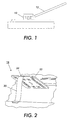
- Such a hinge known as a staple hinge, is illustrated in FIGURE 1 integrally connected with micro-mirror 12, and is used to attain out-of-plane motion.
- the multi-step fabrication process includes depositing a layer which is then patterned and etched.
- a second layer is deposited, patterned and etched in such a way that after removing any filling material, the first layer is free to move in a prescribed path, while being held in place by the second layer.
- This structure creates a rotating joint implemented in MEMS or micro-systems to permit for the mechanical movement required for out-of-plane or vertically oriented devices.
- FIGURE 1 While the described staple hinge provides a useful mechanical function, a drawback is the difficulty to incorporate electrical connections between the hinges and the micro-element to which it is attached.
- FIGURE 1 where it is shown that the lifted structure, i.e. micro-mirror 12 is floating above substrate 14. Providing an electrical connection between these physically separated elements raises significant obstacles to implementing a three-dimensional electrically actuated MEMs device such as an electrostatically driven micro-mirror.
- a three-dimensional electrically actuated MEMs device such as an electrostatically driven micro-mirror.
- a micro-electromechanical assembly including a micro-device formed in the device layer of a silicon-on-insulator substrate.
- a ribbon structure is formed in the same device layer, where the ribbon structure is less than the thickness of the micro-device.
- a connection interface provides a connection point between a first end of the micro-device and a first end of a ribbon structure, wherein the ribbon structure and micro-device are integrated as a single assembly.
- An electrical conductor is formed extending from on end of the ribbon structure to the micro-device tethered at the other end.
- the device layer is formed as part of a silicon-on-insulator wafer, including at least the device layer and a buried oxide layer.
- the ribbon structure has at least one of a width or thickness which is less than at least one of a width or thickness of the out-of-plane device.
- the ribbon hinge is configured with a mechanical integrity which permits application of a lifting out-of-plane mechanical torque to lift the out-of-plane device from 0° which is in the horizontal plane, to 90° or more out of the horizontal plane.
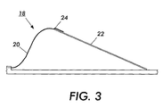
- FIGURES 2 and 3 illustrate a micro-assembly 18 having a ribbon hinge 20 integrated with micro-device 22, such as a micro-mirror.
- micro-device 22 such as a micro-mirror.
- the micro-mirror device 22 has been moved from an inplane position to an angle of approximately 30°. Movement of the mirror is achievable by a variety of mechanisms, including the use of a micro-probe or an actuator.
- Ribbon hinge 20 is, therefore, designed to replace the widely used polysilicon staple-hinge design illustrated in FIGURE 1.
- Ribbon hinge 20 is a single-crystal-silicon (SCS) component which has mechanical stability, and which is configured using a simplified processing procedure.
- SCS single-crystal-silicon
- ribbon hinge 20 of the present invention provides a flexible mechanism as opposed to the jointed staple-hinge of FIGURE 1.
- Ribbon hinge 20 is formed from the device layer of a silicon-on-insulator wafer, which has been thinned down to allow increased mechanical flexibility. This design produces a high quality mechanical structure having sufficient strength for its intended purpose.
- FIGURES 2 and 3 emphasize the flexibility of ribbon hinge 20.
- ribbon hinge 20 is approximately 500nm thick, approximately 50 ⁇ m wide and approximately 140 ⁇ m in length.
- Micro-assembly 18, including ribbon hinge 20 and mirror 22 is fabricated using a silicon-on-insulator (SOI) wafer with a device layer thickness of approximately 3 ⁇ m and a buried oxide (BOX) layer thickness of approximately 2 ⁇ m.
- SOI silicon-on-insulator
- BOX buried oxide
- the bulk area around mirror 22 and other protected areas is etched in a time-etch process leaving approximately 500nm of the device layer silicon.
- the ribbon hinge is then patterned and the exposed surrounding 500nm thick silicon (Si) device layer material is removed in a dry-etch process. This leaves the mirror structure, protected by an oxide layer, and the thin silicon ribbon hinge 20 resting on the sacrificial BOX layer.
- processing e.g. BOX and Hydrofluoric Acid (HF) 49% processing
- HF Hydrofluoric Acid
- a micro-assembly having a ribbon hinge and an integrated micro-device is a two-step process in the sense that in the first step a micro-device, such as mirror 22 is patterned and etched. Then a second procedure is used for thinning down and forming ribbon hinge 20. It is of course possible to inverse these processes by thinning the ribbon layer first and then processing the out-of-plane device area. An issue in this regard is that the micro-device and ribbon hinge are all formed from the same material layer. The difference between the ribbon hinge and micro-device is the geometry of the patterning, and the physical thickness of the areas. Etching ribbon hinge 20 to a much thinner cross-section than micro-device 22, permits increased flexibility of the ribbon hinge 20. The flexibility of ribbon hinge 20 is illustrated by its almost S-shape.
- the methodology that incorporates fabrication of the ribbon hinge structure in the same material as the out-of-plane device such as the mirror, has many advantages over existing hinge technologies, including a simplified fabrication process. For example, since the hinge is fabricated using the same material layer as that of the micro-device, there is no adhesive joint or holding structure necessary between the hinge and the attached micro-device. Such a design accommodates the high mechanical torque and forces delivered by the attached micro-device without comprising the integrity of connection point 24.
- a further advantage of the ribbon hinge configuration discussed above is to use the ribbon hinges for an electrical connection between the ribbon hinge to the micro-device.
- having ribbon hinge and micro-device formed from the same device layer of the silicon-on-insulator wafer allows for the implementation of a three-dimensional electrically actuated MEMs or micro-assembly.
- the fabrication process which permits the placement of an electrical connector from a ribbon hinge to a micro-device is set out in more detail particularly in connection with FIGURES 4-8.
- FIGURE 4 illustrated is a process flow for fabrication of a single crystal silicon ribbon hinge integrated with a micro-device, and having an electrical conductor running from ribbon hinge and to the micro-device, according to the present invention.
- the process begins with a clean silicon-on-insulator (SOI) wafer 30 having a single crystal silicon device layer 32, a buried oxide layer 34, and a substrate layer 36.
- SOI silicon-on-insulator
- a photo-resist layer 40 is deposited on device layer 32 using standard lithographic processes. Photo-resist layer 40 is patterned in such a way as to expose the area to be thinned into the ribbon hinge 42.
- a wet etching process is undertaken such as wet etching with a potassium-hydroxide (KOH) 45% solution at 60°C.
- KOH potassium-hydroxide
- the wet etching causes the exposed ribbon hinge area 42 of device layer 32 to be removed to a thickness of approximately 500nm.
- step 46 previously applied resist layer 40 is removed prior to a repatterning for etching of the out-of-plane device, an island area, an anchor structure and an isolation groove.
- second resist layer 48 is applied on the top surface of SOI 30.
- a dry etching process is undertaken on the exposed silicon of device layer 32 to form the out-of-plane device 52, as well as the island area 54, anchor structure 56 and isolation region or groove 57.
- FIGURE 5 set forth is a top view of step 58 of FIGURE 4.
- Ribbon hinge 42 is shown connected to anchor portion 56 at a first end and to micro-device 52 at a second end.
- Patterned within micro-device 52 is an isolation region 57.
- isolation region 57 is patterned within micro-device 52 to isolate an electrical conductor to be deposited therein from the remainder of micro-device 52.
- an isolation groove may also be patterned within the ribbon structure 42 and anchor 56.
- the additional areas where isolation grooves may be etched are shown in FIGURE 6, which may be considered a further embodiment of the etching process shown in FIGURE 4.
- two isolation regions 57A and 57B are etched into micro-device 52.
- Isolation regions 57C and 57D are also to be etched within ribbon structure 42 through anchor 56.
- FIGURE 6 emphasizes that multiple conductor lines may be processed on a single ribbon hinge 42 and/or micro-device 52. It is also to be understood that multiple ribbon hinges may be attached to a single micro-device.
- step 58 the second layer of photo-resist 48 has been removed, and an etching process is started to begin etching the exposed buried oxide layer 60, using a Hydrofluoric Acid (HF) 49% solution.
- HF Hydrofluoric Acid
- step 62 the third and final layer of photo-resist 64 is deposited and patterned on the SOI wafer 30.
- This final photo-resist layer 64 is to be used during the buried oxide-release (BOX) operation, wherein ribbon hinge 42 and micro-device 52 are released by etching all unprotected buried oxide.
- a depositing step deposits an electrical conductive material 65 within isolation region 57 and on ribbon structure 42. It is to be understood that same conductive material may be deposited within the isolation regions 57A-57D of FIGURE 6.
- the buried oxide release (BOX) operation is undertaken, whereafter, as shown in step 66 of FIGURE 4, the only remaining buried oxide layer material 68 and 70 is under the island structure 54 and the anchor section 56.
- the remaining buried oxide material is removed such that a separation layer 72 and separation edge 74 are void of such material. Removal of the buried oxide allows for the movement of the micro-device 52 and ribbon hinge 42.
- step 68 it is noted that all remaining photo-resist is removed, for example by a dry O 2 plasma-etch process.
- step 68 depicts the original SOI wafer 30 as a micro-device and hinge assembly, with a conductor.
- FIGURE 8 set forth is a completed micro-assembly 80 according to the teachings of the present invention. More particularly, a ribbon hinge 42 as described in the foregoing, is integrally attached at a first end to a micro-device 52 and at a second end to an anchor portion 56.
- Micro-device 52 includes an etched isolation region 57. Deposited within isolation region 57 is a conductive material 65 which is also deposited on ribbon hinge 42 and within an isolation groove of anchor 56.
- An electronic device 76 is in operational connection to the electrical conductor material 65 within isolation region 57.
- a power source 78 is in connection with the electrical conductor material 65, at an opposite end by anchor portion 56. Electronic device 76 may be activated upon application of electrical power from electrical power source 78. Further, electrical device 76 may be any one of a number of devices such as an actuator to assist in movement of micro-device 52.
Landscapes
- Engineering & Computer Science (AREA)
- Computer Hardware Design (AREA)
- Microelectronics & Electronic Packaging (AREA)
- Micromachines (AREA)
- Pressure Sensors (AREA)
- Mechanical Light Control Or Optical Switches (AREA)
Abstract
Description
Claims (10)
- A hinge for use in a micro-assembly employing electrical power supplied from an electrical power source, the hinge comprising:a silicon-on-insulator wafer including a bottom substrate layer, a middle buried oxide layer and a single crystal silicon device layer;a ribbon hinge structure formed in the device layer of the silicon-on-insulator wafer, wherein the ribbon hinge structure is flexible and capable of movement out of the plane of the device layer; andan electrical conductor carried on at least a portion of a surface of the ribbon hinge.
- The invention according to claim 1 wherein the out-of-plane device is fabricated from a silicon-on-insulator wafer which has an initial uniform device layer thickness.
- The invention according to claim 1 wherein the ribbon is configured with a mechanical integrity which permits application of a side-twisting mechanical torque sufficient to twist the ribbon hinge to 90° or more from an initial 0° twisted position.
- The invention according to claim 1 wherein the ribbon structure has at least one of a width or thickness which is less than at least one of a width or thickness of the out-of-plane device.
- The invention according to claim 1 wherein the ribbon hinge has at least one of (i) an isolation region formed within the ribbon hinge, and within which is deposited the electrical conduction material, or (ii) an area of insulation material which has been deposited and then patterned on the ribbon hinge area, wherein conductors can then be placed on top of the insulator material.
- A micro-assembly comprising:a micro-device formed on or in the device layer of a single crystal silicon substrate;a ribbon hinge formed on the device layer, the ribbon structure having been thinned to a thickness which is less than the thickness of the micro-device;a connection interface providing a connection point between a first end of the out-of-plane device and a first end of the ribbon hinge; andan electrical conductor material extending along the ribbon structure toward the micro-device.
- The invention according to claim 6 further including an anchor portion holding one end of the ribbon hinge in a secure position.
- The invention according to claim 7 where the anchor portion is formed with an isolation groove, within which is deposited the isolation region of the anchor portion.
- The invention according to claim 6 wherein the micro-device includes an isolation region, formed within the micro-device, and in which the electrical conductive material is deposited.
- The invention according to claim 6 further including an isolation region formed within the ribbon hinge, and within which is deposited the electrical conductive material.
Applications Claiming Priority (2)
| Application Number | Priority Date | Filing Date | Title |
|---|---|---|---|
| US09/725,836 US6756545B2 (en) | 2000-11-29 | 2000-11-29 | Micro-device assembly with electrical capabilities |
| US725836 | 2000-11-29 |
Publications (3)
| Publication Number | Publication Date |
|---|---|
| EP1211218A2 true EP1211218A2 (en) | 2002-06-05 |
| EP1211218A3 EP1211218A3 (en) | 2003-01-08 |
| EP1211218B1 EP1211218B1 (en) | 2007-08-15 |
Family
ID=24916152
Family Applications (1)
| Application Number | Title | Priority Date | Filing Date |
|---|---|---|---|
| EP01127498A Expired - Lifetime EP1211218B1 (en) | 2000-11-29 | 2001-11-28 | Micro-device assembly with electrical capabilities |
Country Status (4)
| Country | Link |
|---|---|
| US (1) | US6756545B2 (en) |
| EP (1) | EP1211218B1 (en) |
| JP (1) | JP2002219698A (en) |
| DE (1) | DE60129914T2 (en) |
Families Citing this family (2)
| Publication number | Priority date | Publication date | Assignee | Title |
|---|---|---|---|---|
| US7190854B1 (en) * | 2000-05-24 | 2007-03-13 | Active Optical Networks, Inc. | Methods for forming an array of MEMS optical elements |
| JP6467347B2 (en) * | 2013-11-07 | 2019-02-13 | 住友精密工業株式会社 | Semiconductor device |
Family Cites Families (21)
| Publication number | Priority date | Publication date | Assignee | Title |
|---|---|---|---|---|
| US5490034A (en) | 1989-01-13 | 1996-02-06 | Kopin Corporation | SOI actuators and microsensors |
| US5245504A (en) | 1989-02-28 | 1993-09-14 | United Technologies Corporation | Methodology for manufacturing hinged diaphragms for semiconductor sensors |
| US5006487A (en) | 1989-07-27 | 1991-04-09 | Honeywell Inc. | Method of making an electrostatic silicon accelerometer |
| US5069742A (en) | 1990-02-05 | 1991-12-03 | Bleil Carl E | Method and apparatus for crystal ribbon growth |
| US5311360A (en) | 1992-04-28 | 1994-05-10 | The Board Of Trustees Of The Leland Stanford, Junior University | Method and apparatus for modulating a light beam |
| US5369544A (en) | 1993-04-05 | 1994-11-29 | Ford Motor Company | Silicon-on-insulator capacitive surface micromachined absolute pressure sensor |
| US5629790A (en) | 1993-10-18 | 1997-05-13 | Neukermans; Armand P. | Micromachined torsional scanner |
| US5962949A (en) * | 1996-12-16 | 1999-10-05 | Mcnc | Microelectromechanical positioning apparatus |
| US5903380A (en) | 1997-05-01 | 1999-05-11 | Rockwell International Corp. | Micro-electromechanical (MEM) optical resonator and method |
| US5870007A (en) | 1997-06-16 | 1999-02-09 | Roxburgh Ltd. | Multi-dimensional physical actuation of microstructures |
| US6074890A (en) | 1998-01-08 | 2000-06-13 | Rockwell Science Center, Llc | Method of fabricating suspended single crystal silicon micro electro mechanical system (MEMS) devices |
| US6046659A (en) * | 1998-05-15 | 2000-04-04 | Hughes Electronics Corporation | Design and fabrication of broadband surface-micromachined micro-electro-mechanical switches for microwave and millimeter-wave applications |
| US6153839A (en) * | 1998-10-22 | 2000-11-28 | Northeastern University | Micromechanical switching devices |
| US6243194B1 (en) | 1998-12-18 | 2001-06-05 | Eastman Kodak Company | Electro-mechanical grating device |
| US6236491B1 (en) * | 1999-05-27 | 2001-05-22 | Mcnc | Micromachined electrostatic actuator with air gap |
| US6229683B1 (en) * | 1999-06-30 | 2001-05-08 | Mcnc | High voltage micromachined electrostatic switch |
| US6057520A (en) * | 1999-06-30 | 2000-05-02 | Mcnc | Arc resistant high voltage micromachined electrostatic switch |
| US6275320B1 (en) * | 1999-09-27 | 2001-08-14 | Jds Uniphase, Inc. | MEMS variable optical attenuator |
| US6267605B1 (en) | 1999-11-15 | 2001-07-31 | Xerox Corporation | Self positioning, passive MEMS mirror structures |
| US6303885B1 (en) * | 2000-03-03 | 2001-10-16 | Optical Coating Laboratory, Inc. | Bi-stable micro switch |
| US6456420B1 (en) | 2000-07-27 | 2002-09-24 | Mcnc | Microelectromechanical elevating structures |
-
2000
- 2000-11-29 US US09/725,836 patent/US6756545B2/en not_active Expired - Fee Related
-
2001
- 2001-11-22 JP JP2001356891A patent/JP2002219698A/en active Pending
- 2001-11-28 DE DE60129914T patent/DE60129914T2/en not_active Expired - Lifetime
- 2001-11-28 EP EP01127498A patent/EP1211218B1/en not_active Expired - Lifetime
Also Published As
| Publication number | Publication date |
|---|---|
| EP1211218B1 (en) | 2007-08-15 |
| EP1211218A3 (en) | 2003-01-08 |
| US20020063339A1 (en) | 2002-05-30 |
| DE60129914T2 (en) | 2007-12-06 |
| US6756545B2 (en) | 2004-06-29 |
| DE60129914D1 (en) | 2007-09-27 |
| JP2002219698A (en) | 2002-08-06 |
Similar Documents
| Publication | Publication Date | Title |
|---|---|---|
| US7083997B2 (en) | Bonded wafer optical MEMS process | |
| US6563106B1 (en) | Micro-electro-mechanical-system (MEMS) mirror device and methods for fabricating the same | |
| AU7389900A (en) | Microelectromechanical optical switch and method of manufacture thereof | |
| US6887391B1 (en) | Fabrication and controlled release of structures using etch-stop trenches | |
| TW201034933A (en) | Microelectromechanical device with isolated microstructures and method of producing same | |
| CN1296191A (en) | Integrated photoelectronic device with ejected reflection mirror and foration and operation method | |
| CN101917175B (en) | Micro-electro-mechanical-system (mems) resonator and manufacturing method thereof | |
| CN1278326A (en) | Microelectromechanical positioning apparatus | |
| JP2007535797A (en) | Beam for micromachine technology (MEMS) switches | |
| JP5579118B2 (en) | Mechanical switch with curved bilayer | |
| US7253550B2 (en) | Torsional electrostatic actuator | |
| US6654155B2 (en) | Single-crystal-silicon ribbon hinges for micro-mirror and MEMS assembly on SOI material | |
| CN101597021B (en) | Method for structuring a device layer of a substrate | |
| US6756545B2 (en) | Micro-device assembly with electrical capabilities | |
| JP2010228094A (en) | Micro-channel device and method for forming micro-channel device layer | |
| US20130273683A1 (en) | Method of Fabricating An Electromechanical Structure Including at Least One Mechanical Reinforcing Pillar | |
| JP2003260697A (en) | Out-of-plane operating method for thermal mems actuator and thermal mems actuator | |
| EP1333008B1 (en) | Systems and methods for thermal isolation of a silicon structure | |
| EP1640334B1 (en) | An integrated lid formed on mems device | |
| US6727436B2 (en) | Interconnect bus crossover for MEMS |
Legal Events
| Date | Code | Title | Description |
|---|---|---|---|
| PUAI | Public reference made under article 153(3) epc to a published international application that has entered the european phase |
Free format text: ORIGINAL CODE: 0009012 |
|
| AK | Designated contracting states |
Kind code of ref document: A2 Designated state(s): AT BE CH CY DE DK ES FI FR GB GR IE IT LI LU MC NL PT SE TR |
|
| AX | Request for extension of the european patent |
Free format text: AL;LT;LV;MK;RO;SI |
|
| PUAL | Search report despatched |
Free format text: ORIGINAL CODE: 0009013 |
|
| AK | Designated contracting states |
Kind code of ref document: A3 Designated state(s): AT BE CH CY DE DK ES FI FR GB GR IE IT LI LU MC NL PT SE TR |
|
| AX | Request for extension of the european patent |
Free format text: AL;LT;LV;MK;RO;SI |
|
| 17P | Request for examination filed |
Effective date: 20030708 |
|
| AKX | Designation fees paid |
Designated state(s): DE FR GB |
|
| 17Q | First examination report despatched |
Effective date: 20040211 |
|
| GRAP | Despatch of communication of intention to grant a patent |
Free format text: ORIGINAL CODE: EPIDOSNIGR1 |
|
| GRAS | Grant fee paid |
Free format text: ORIGINAL CODE: EPIDOSNIGR3 |
|
| GRAA | (expected) grant |
Free format text: ORIGINAL CODE: 0009210 |
|
| AK | Designated contracting states |
Kind code of ref document: B1 Designated state(s): DE FR GB |
|
| REG | Reference to a national code |
Ref country code: GB Ref legal event code: FG4D |
|
| REF | Corresponds to: |
Ref document number: 60129914 Country of ref document: DE Date of ref document: 20070927 Kind code of ref document: P |
|
| ET | Fr: translation filed | ||
| PLBE | No opposition filed within time limit |
Free format text: ORIGINAL CODE: 0009261 |
|
| STAA | Information on the status of an ep patent application or granted ep patent |
Free format text: STATUS: NO OPPOSITION FILED WITHIN TIME LIMIT |
|
| 26N | No opposition filed |
Effective date: 20080516 |
|
| PGFP | Annual fee paid to national office [announced via postgrant information from national office to epo] |
Ref country code: DE Payment date: 20141023 Year of fee payment: 14 Ref country code: GB Payment date: 20141024 Year of fee payment: 14 |
|
| PGFP | Annual fee paid to national office [announced via postgrant information from national office to epo] |
Ref country code: FR Payment date: 20141124 Year of fee payment: 14 |
|
| REG | Reference to a national code |
Ref country code: DE Ref legal event code: R119 Ref document number: 60129914 Country of ref document: DE |
|
| GBPC | Gb: european patent ceased through non-payment of renewal fee |
Effective date: 20151128 |
|
| REG | Reference to a national code |
Ref country code: FR Ref legal event code: ST Effective date: 20160729 |
|
| PG25 | Lapsed in a contracting state [announced via postgrant information from national office to epo] |
Ref country code: DE Free format text: LAPSE BECAUSE OF NON-PAYMENT OF DUE FEES Effective date: 20160601 Ref country code: GB Free format text: LAPSE BECAUSE OF NON-PAYMENT OF DUE FEES Effective date: 20151128 |
|
| PG25 | Lapsed in a contracting state [announced via postgrant information from national office to epo] |
Ref country code: FR Free format text: LAPSE BECAUSE OF NON-PAYMENT OF DUE FEES Effective date: 20151130 |