EP1209959A2 - Multilayer circuit board and method of manufacturing the same - Google Patents
Multilayer circuit board and method of manufacturing the same Download PDFInfo
- Publication number
- EP1209959A2 EP1209959A2 EP01126948A EP01126948A EP1209959A2 EP 1209959 A2 EP1209959 A2 EP 1209959A2 EP 01126948 A EP01126948 A EP 01126948A EP 01126948 A EP01126948 A EP 01126948A EP 1209959 A2 EP1209959 A2 EP 1209959A2
- Authority
- EP
- European Patent Office
- Prior art keywords
- layer
- multilayer circuit
- substrate
- conductive layer
- set forth
- Prior art date
- Legal status (The legal status is an assumption and is not a legal conclusion. Google has not performed a legal analysis and makes no representation as to the accuracy of the status listed.)
- Withdrawn
Links
Images


Classifications
-
- H—ELECTRICITY
- H05—ELECTRIC TECHNIQUES NOT OTHERWISE PROVIDED FOR
- H05K—PRINTED CIRCUITS; CASINGS OR CONSTRUCTIONAL DETAILS OF ELECTRIC APPARATUS; MANUFACTURE OF ASSEMBLAGES OF ELECTRICAL COMPONENTS
- H05K3/00—Apparatus or processes for manufacturing printed circuits
- H05K3/46—Manufacturing multilayer circuits
-
- H—ELECTRICITY
- H05—ELECTRIC TECHNIQUES NOT OTHERWISE PROVIDED FOR
- H05K—PRINTED CIRCUITS; CASINGS OR CONSTRUCTIONAL DETAILS OF ELECTRIC APPARATUS; MANUFACTURE OF ASSEMBLAGES OF ELECTRICAL COMPONENTS
- H05K1/00—Printed circuits
- H05K1/18—Printed circuits structurally associated with non-printed electric components
- H05K1/182—Printed circuits structurally associated with non-printed electric components associated with components mounted in the printed circuit board, e.g. insert mounted components [IMC]
- H05K1/183—Components mounted in and supported by recessed areas of the printed circuit board
-
- H—ELECTRICITY
- H05—ELECTRIC TECHNIQUES NOT OTHERWISE PROVIDED FOR
- H05K—PRINTED CIRCUITS; CASINGS OR CONSTRUCTIONAL DETAILS OF ELECTRIC APPARATUS; MANUFACTURE OF ASSEMBLAGES OF ELECTRICAL COMPONENTS
- H05K1/00—Printed circuits
- H05K1/02—Details
- H05K1/11—Printed elements for providing electric connections to or between printed circuits
- H05K1/119—Details of rigid insulating substrates therefor, e.g. three-dimensional details
-
- H—ELECTRICITY
- H05—ELECTRIC TECHNIQUES NOT OTHERWISE PROVIDED FOR
- H05K—PRINTED CIRCUITS; CASINGS OR CONSTRUCTIONAL DETAILS OF ELECTRIC APPARATUS; MANUFACTURE OF ASSEMBLAGES OF ELECTRICAL COMPONENTS
- H05K3/00—Apparatus or processes for manufacturing printed circuits
- H05K3/40—Forming printed elements for providing electric connections to or between printed circuits
- H05K3/403—Edge contacts; Windows or holes in the substrate having plural connections on the walls thereof
-
- H—ELECTRICITY
- H05—ELECTRIC TECHNIQUES NOT OTHERWISE PROVIDED FOR
- H05K—PRINTED CIRCUITS; CASINGS OR CONSTRUCTIONAL DETAILS OF ELECTRIC APPARATUS; MANUFACTURE OF ASSEMBLAGES OF ELECTRICAL COMPONENTS
- H05K3/00—Apparatus or processes for manufacturing printed circuits
- H05K3/46—Manufacturing multilayer circuits
- H05K3/4697—Manufacturing multilayer circuits having cavities, e.g. for mounting components
-
- B—PERFORMING OPERATIONS; TRANSPORTING
- B29—WORKING OF PLASTICS; WORKING OF SUBSTANCES IN A PLASTIC STATE IN GENERAL
- B29L—INDEXING SCHEME ASSOCIATED WITH SUBCLASS B29C, RELATING TO PARTICULAR ARTICLES
- B29L2031/00—Other particular articles
- B29L2031/34—Electrical apparatus, e.g. sparking plugs or parts thereof
- B29L2031/3493—Moulded interconnect devices, i.e. moulded articles provided with integrated circuit traces
-
- H—ELECTRICITY
- H05—ELECTRIC TECHNIQUES NOT OTHERWISE PROVIDED FOR
- H05K—PRINTED CIRCUITS; CASINGS OR CONSTRUCTIONAL DETAILS OF ELECTRIC APPARATUS; MANUFACTURE OF ASSEMBLAGES OF ELECTRICAL COMPONENTS
- H05K1/00—Printed circuits
- H05K1/02—Details
- H05K1/0284—Details of three-dimensional rigid printed circuit boards
-
- H—ELECTRICITY
- H05—ELECTRIC TECHNIQUES NOT OTHERWISE PROVIDED FOR
- H05K—PRINTED CIRCUITS; CASINGS OR CONSTRUCTIONAL DETAILS OF ELECTRIC APPARATUS; MANUFACTURE OF ASSEMBLAGES OF ELECTRICAL COMPONENTS
- H05K2201/00—Indexing scheme relating to printed circuits covered by H05K1/00
- H05K2201/09—Shape and layout
- H05K2201/09009—Substrate related
- H05K2201/09036—Recesses or grooves in insulating substrate
-
- H—ELECTRICITY
- H05—ELECTRIC TECHNIQUES NOT OTHERWISE PROVIDED FOR
- H05K—PRINTED CIRCUITS; CASINGS OR CONSTRUCTIONAL DETAILS OF ELECTRIC APPARATUS; MANUFACTURE OF ASSEMBLAGES OF ELECTRICAL COMPONENTS
- H05K2201/00—Indexing scheme relating to printed circuits covered by H05K1/00
- H05K2201/09—Shape and layout
- H05K2201/09009—Substrate related
- H05K2201/09045—Locally raised area or protrusion of insulating substrate
-
- H—ELECTRICITY
- H05—ELECTRIC TECHNIQUES NOT OTHERWISE PROVIDED FOR
- H05K—PRINTED CIRCUITS; CASINGS OR CONSTRUCTIONAL DETAILS OF ELECTRIC APPARATUS; MANUFACTURE OF ASSEMBLAGES OF ELECTRICAL COMPONENTS
- H05K2201/00—Indexing scheme relating to printed circuits covered by H05K1/00
- H05K2201/09—Shape and layout
- H05K2201/09009—Substrate related
- H05K2201/09118—Moulded substrate
-
- H—ELECTRICITY
- H05—ELECTRIC TECHNIQUES NOT OTHERWISE PROVIDED FOR
- H05K—PRINTED CIRCUITS; CASINGS OR CONSTRUCTIONAL DETAILS OF ELECTRIC APPARATUS; MANUFACTURE OF ASSEMBLAGES OF ELECTRICAL COMPONENTS
- H05K2201/00—Indexing scheme relating to printed circuits covered by H05K1/00
- H05K2201/09—Shape and layout
- H05K2201/09145—Edge details
- H05K2201/0919—Exposing inner circuit layers or metal planes at the side edge of the PCB or at the walls of large holes
-
- H—ELECTRICITY
- H05—ELECTRIC TECHNIQUES NOT OTHERWISE PROVIDED FOR
- H05K—PRINTED CIRCUITS; CASINGS OR CONSTRUCTIONAL DETAILS OF ELECTRIC APPARATUS; MANUFACTURE OF ASSEMBLAGES OF ELECTRICAL COMPONENTS
- H05K2201/00—Indexing scheme relating to printed circuits covered by H05K1/00
- H05K2201/09—Shape and layout
- H05K2201/09209—Shape and layout details of conductors
- H05K2201/095—Conductive through-holes or vias
- H05K2201/09645—Patterning on via walls; Plural lands around one hole
-
- H—ELECTRICITY
- H05—ELECTRIC TECHNIQUES NOT OTHERWISE PROVIDED FOR
- H05K—PRINTED CIRCUITS; CASINGS OR CONSTRUCTIONAL DETAILS OF ELECTRIC APPARATUS; MANUFACTURE OF ASSEMBLAGES OF ELECTRICAL COMPONENTS
- H05K3/00—Apparatus or processes for manufacturing printed circuits
- H05K3/02—Apparatus or processes for manufacturing printed circuits in which the conductive material is applied to the surface of the insulating support and is thereafter removed from such areas of the surface which are not intended for current conducting or shielding
- H05K3/027—Apparatus or processes for manufacturing printed circuits in which the conductive material is applied to the surface of the insulating support and is thereafter removed from such areas of the surface which are not intended for current conducting or shielding the conductive material being removed by irradiation, e.g. by photons, alpha or beta particles
-
- H—ELECTRICITY
- H05—ELECTRIC TECHNIQUES NOT OTHERWISE PROVIDED FOR
- H05K—PRINTED CIRCUITS; CASINGS OR CONSTRUCTIONAL DETAILS OF ELECTRIC APPARATUS; MANUFACTURE OF ASSEMBLAGES OF ELECTRICAL COMPONENTS
- H05K3/00—Apparatus or processes for manufacturing printed circuits
- H05K3/46—Manufacturing multilayer circuits
- H05K3/4644—Manufacturing multilayer circuits by building the multilayer layer by layer, i.e. build-up multilayer circuits
-
- Y—GENERAL TAGGING OF NEW TECHNOLOGICAL DEVELOPMENTS; GENERAL TAGGING OF CROSS-SECTIONAL TECHNOLOGIES SPANNING OVER SEVERAL SECTIONS OF THE IPC; TECHNICAL SUBJECTS COVERED BY FORMER USPC CROSS-REFERENCE ART COLLECTIONS [XRACs] AND DIGESTS
- Y10—TECHNICAL SUBJECTS COVERED BY FORMER USPC
- Y10T—TECHNICAL SUBJECTS COVERED BY FORMER US CLASSIFICATION
- Y10T29/00—Metal working
- Y10T29/49—Method of mechanical manufacture
- Y10T29/49002—Electrical device making
- Y10T29/49117—Conductor or circuit manufacturing
- Y10T29/49124—On flat or curved insulated base, e.g., printed circuit, etc.
- Y10T29/49155—Manufacturing circuit on or in base
Definitions
- the present invention relates to a multilayer circuit board, and particularly a molded interconnect device (MID) having a multilayer circuit of a reduced thickness, in which a layer-to-layer connection(s) is formed with high reliability, and a method of manufacturing the same.
- MID molded interconnect device
- a molded interconnect device obtained by three-dimensionally forming circuit patterns on an injection-molded substrate receives attention from the viewpoint of reductions in weight and size of electronic devices, and for the purpose of improving a degree of flexibility in circuit design and achieving high-density wiring.
- Japanese Patent Early Publication No. 7-170077 discloses a method of manufacturing injection-molded circuit parts.
- a plurality of injection-molded circuit members (1P, 2P) are previously produced.
- Each of the circuit members has conductive circuit patterns (5P, 6P) on its top and bottom surfaces.
- each of the circuit members has a positioning hole 10P, spacing projections 11P and recesses 12P for receiving the spacing projections.
- These circuit members are laminated such that the spacing projection 11P of the circuit member 1P is inserted into the corresponding recess 12P of the adjacent circuit member 2P, to obtain a multilayer circuit structure.
- Positions of the respective circuit members in the multilayer circuit structure are determined by allowing a positioning pin 14P to pass through the positioning holes 10P.
- a clearance between adjacent circuit members (1P, 2P) of the multilayer circuit structure is filled with an insulating resin 20P, and an electrically conductive film 30P is formed in a through-hole obtained by removing the pin 14P from the positioning holes 10P to obtain a layer-to-layer connection in the multilayer circuit structure, as shown in FIG. 19B.
- Japanese Patent Early Publication No. 7-249873 discloses a multilayer-circuit molded article and a method of manufacturing the same.
- a resin-molded inner substrate 1S having protrusions 2S on its top and bottom surfaces is formed.
- first circuit patterns (3S, 4S) are formed at required regions on the top and bottom surfaces of the inner substrate 1S by electroless plating.
- a resin-molded outer substrate 5S is formed on the inner substrate 1S by injection molding such that only the first circuit patterns on the top surfaces of the protrusions 2S of the inner substrate 1S are exposed outside, as shown in FIG. 20B.
- second circuit patterns 8S are formed at required regions on the outer substrate 5S by electroless plating.
- the second circuit patterns 8S can be connected to the first circuit patterns ( 3S , 4S ) on the protrusions 2S to make a layer-to-layer connection between the inner and outer substrates ( 1S , 5S ).
- an electrical connection between the second circuit patterns 8S on the top and bottom surfaces of the outer substrate 5S can be made by a through-hole plating 6S .
- a concern of the present invention is to provide a multilayer circuit board, and particularly a molded interconnect device (MID) having a multilayer circuit of a reduced thickness, in which a layer-to-layer connection(s) is formed with high reliability.
- MID molded interconnect device
- the multilayer circuit board of the present invention comprises:
- the second surface of the substrate is a side surface of a projection on the first surface.
- the substrate has a third surface extending at a different level from the first surface and a fourth surface extending from the other end of the first surface to an end of the third surface, and the multilayer circuit is formed on the first, third and fourth surfaces of the substrate, and the second conductive layer is formed on a side surface of a projection on the first surface to make the layer-to-layer connection of the multilayer circuit.
- a substrate for MID for example, a substrate used in a first embodiment of the present invention and having configurations shown in FIG.
- each of second conductive layers is separated from an adjacent second conductive layer in the thickness direction by a second insulation layer.
- the first surface is a top surface of the substrate, and the second surface is a side surface of the substrate.
- the multilayer circuit has an aperture, through which a part of the first surface is exposed, and an electronic device is mounted in a concave formed in the exposed first surface, and an electrical connection between the multilayer circuit and the electronic device is made by a third conductive layer formed on an inner surface of the concave.
- Another concern of the present invention is to provide a method of manufacturing the multilayer circuit board described above. That is, the method comprises the steps of:
- the first surface is a top surface of the substrate
- the second surface is a side surface of a projection on the first surface
- the second conductive layer is formed on the side surface of the projection during the circuit-layer forming steps.
- the second conductive layer is obtained by cutting the substrate having the multilayer circuit such that a cutting surface of the multilayer circuit is flush with the cutting surface of the substrate, and forming a conductive film for the layer-to-layer connection on the cutting surfaces of the multilayer circuit and the substrate.
- a multilayer circuit board of the first embodiment of the present invention can be manufactured by the following method.
- a resin-molded substrate 10 for MID (molded interconnect device) is prepared. As shown in FIG. 1A, this substrate 10 has, on its top surface, a first surface 11, a first projection 13 on the first surface, second surface 14 extending at a different level from the first surface, second projection 17 on the second surface, and a third surface 16 extending between the first and second surfaces (11, 14) in a substantially vertical direction.
- the substrate for MID can be three-dimensionally produced by means of injection molding.
- the resin material for example, it is possible to use polyphenylene sulfide (PPS), liquid-crystal polymer (LCP), syndiotactic polystyrene (SPS), or polyphthal amide (PPA).
- a filler such as inorganic fibers may be added into the resin material to improve the mechanical strength of the substrate.
- a ceramic substrate can be used as the substrate for MID.
- the ceramic substrate for MID can be produced by injection-molding a ceramic powder such as alumina (Al 2 O 3 ) to obtain a molded article having a required three-dimensional shape, and sintering the molded article.
- a multilayer circuit board of the present invention can be manufactured by forming a multilayer circuit on the ceramic substrate for MID.
- the first conductive layer 20 having a desired circuit pattern is formed on the substrate 10.
- the first conductive layer 20 can be obtained by forming a copper film 20a on the entire top surface of the substrate 10 by spattering or CVD (Chemical Vapor Deposition), as shown in FIG. 1B, removing a required region of the copper film 20a by use of a laser beam to obtain a copper-film pattern 20b on the substrate 10 (FIG. 1C), and electro-plating copper on the copper-film pattern 20b (FIG. 1D).
- the copper film 20a has a thickness of 0.1 to 0.5 ⁇ m.
- the copper-film pattern can be easily formed by laser patterning, and the subsequent electro-plating is facilitated.
- the copper film 20a on the first projection 13 and a part of the copper film 20a on the first surface 11 are removed to obtain the copper-film pattern 20b.
- a first insulation layer 30 is formed on the entire top surface of the substrate of FIG. 1D.
- the first insulation layer 30 can be formed by means of film formation, for example, a method of applying an insulation material on the substrate 10 of FIG. 1D with the first conductive layer 20, a method of adhering an insulation film on the substrate 10, or a deposition polymerization method.
- required regions of the first insulation layer 30 are removed.
- the insulation material of the first insulation layer 30 is removed from the first projection 13 and the second projection 17.
- the step of removing the insulation material can be carried out by use of a laser beam or a focused ion beam.
- the second conductive layer 22 can be obtained by forming a copper film 22a on the entire top surface of the substrate of FIG. 2B by spattering or CVD (FIG. 2C), removing a required region of the copper film 22a by use of a laser beam to obtain a copper-film pattern 22b (FIG. 2D), and electro-plating copper on the copper-film pattern 22b (FIG. 3A).
- a part of the copper film 22a is removed from the second projection 17 to form the copper-film pattern 22b.
- a second insulation layer 32 is formed on the entire top surface of the substrate of FIG. 3A, as shown in FIG. 3B.
- the above-described method of forming the first insulation layer 30 is available to form the second insulation layer 32.
- required regions of the second insulation layer 32 are removed.
- the insulation material of the second insulation layer 32 is removed from the first projection 13 and the second projection 17.
- a third conductive layer 24 having a desired circuit pattern is formed.
- the above-described method of forming the first or second conductive layer (20, 22) is available to form the third conductive layer 24.
- an end of the third conductive layer 24 makes contact with the first conductive layer 20 on the side surface 15 of the second projection 17. Therefore, the first conductive layer 20 on the side surface 15 of the second projection 17 provides a layer-to-layer connection between the first conductive layer and third conductive layers (20, 24) of the multilayer circuit.
- a third insulation layer 34 is formed on the entire top surface of the substrate of FIG. 3D. Subsequently, required regions of the third insulation layer 34 are removed. In this embodiment, as shown in FIG. 4A, the insulation material of the third insulation layer 34 is removed from the first and second projections (13, 17) to expose the second conductive layer 22 and the first conductive layer 20, respectively.
- a fourth conductive layer 26 having a desired circuit pattern is formed.
- the above-described method of forming the first or second conductive layer (20, 22) is available to form the fourth conductive layer 26.
- an end of the fourth conductive layer 26 makes contact with the second conductive layer 22 on the first projection 13. Therefore, the second conductive layer 22 on the side surface 12 of the first projection 13 provides a layer-to-layer connection between the second and fourth conductive layers (22, 26) of the multilayer circuit.
- an end of the fourth conductive layer 26 makes contact with the first conductive layer 20 on the second projection 17. Therefore, the first conductive layer 20 on the side surface 15 of the second projection 17 provides a layer-to-layer connection between the first, third and fourth conductive layers (20, 24, 26) of the multilayer circuit, as shown in FIG. 4C.
- the multilayer circuit board of this embodiment is produced such that each of the conductive layers (20, 22, 24) is spaced from the adjacent conductive layer by a multilayer insulating structure 3, as shown in FIG. 4C. That is, in this embodiment, the multilayer insulating structure 3 is composed of the first insulation layer 30, the second insulation layer 32, which is connected to a part of the first insulation layer, and the third insulation layer 34, which is connected to a part of the second insulation layer.
- each of the conductive layers (20, 22, 24, 26) and the insulation layers (30, 32, 34) is formed by means of film formation, it is possible to provide the multilayer circuit having a reduced thickness.
- the outermost conductive layer 26 of the multilayer circuit has a thickness of 10 to 30 ⁇ m, which can be formed by performing electro-plating of copper, gold or nickel on the thin copper film.
- each of the inner conductive layers (20, 22, 24) of the multilayer circuit has a smaller thickness than the outermost conductive layer 26.
- each of the inner conductive layers has a thickness of 0.5 to 10 ⁇ m. Therefore, if necessary, the inner conductive layer may be formed by only a thin copper film without the subsequent electro-plating.
- the insulation layer (30, 32, 34) can be formed by use of epoxy resins or polyimide resins. It is preferred that of the each of the insulation layers (30, 32, 34) has a thickness of 50 ⁇ m or less, which means a thickness of the insulation layer formed on the circuit pattern of the conductive layer, but does not mean the thickness of the insulation layer filled in concaves that are formed by removing required regions of the conductive layer to obtain the circuit pattern of the conductive layer. In addition, when the multilayer circuit having a reduced thickness is needed, it is preferred that each of the insulation layers has a thickness of 5 to 20 ⁇ m to avoid the occurrence of insulation failures such as pinholes.
- the multilayer circuit board of a reduced thickness can be manufactured, as compared with the case of stacking a plurality of resin-molded circuit boards having conductive patterns, as disclosed in Japanese Patent Early Publication No. 7-170077.
- the conductive layer formed on the side surface of the projection of the substrate is used for the layer-to-layer connection of the multilayer circuit, there is an advantage that the formation of the layer-to-layer connection between the conductive layers can be carried out simultaneously with the formation of the conductive layer of the multilayer circuit.
- the multilayer circuit is composed of four conductive layers (20, 22, 24, 26) and three insulation layers (30, 32, 34).
- the numbers of the conductive layers and the insulation layers in the multilayer circuit, the number of the projections, and the position and size of the respective projection can be optionally determined according to circuit designs to be needed in the multilayer circuit.
- the insulation layer can be formed by deposition polymerization or plasma polymerization.
- the insulation layer may be obtained by forming a film of an insulating resin having photocurability, and curing the film under light irradiation such as ultraviolet.
- light irradiation such as ultraviolet
- an insulation film may be formed by thermo-compression bonding an insulating resin sheet having apertures at positions corresponding to the projections on the substrate.
- an insulation resin film may be formed on the conductive layer by means of electro-deposition.
- each of the first and second projections (13, 17) has a tapered tip.
- the side surface of the projection is an inclined surface by an obtuse angle relative to the horizontal surface of the substrate, there is an advantage that the irradiation angle of a laser beam 50 or a focused ion beam can be easily set.
- the electric-field strength increases at the vicinity of the tapered tip, and oxygen ions in the plasma are concentrated onto the projection.
- a higher etching rate of the insulation material is obtained on the projection than the flat-surface portion. Therefore, by exposing the insulation film on the projection to the plasma, it is possible to readily remove the insulation film from the projection.
- the insulation film Before the formation of the insulation film, it is preferred to perform a surface-modification treatment for giving water repellency or oil repellency to the projection surface, for example, fluoridization treatment using CF 4 ions. In this case, the step of removing the insulation layer from the projection can be further enhanced.
- the conductive layer may be formed on only desired regions of the substrate by spraying aerosol-like copper fine particles, or using a laser CVD. In these cases, it is possible to omit the step of etching the conductive film to obtain the required circuit pattern.
- a multilayer circuit board according to a second embodiment of the present invention is explained in detail below.
- FIG. 6 shows a cross-sectional view of the multilayer circuit board of the second embodiment.
- This multilayer circuit board comprises a substrate 10 having a first surface 14 that is a horizontal surface and a second surface 15 projecting in a substantially vertical direction from one side of the first surface, a multilayer circuit formed on the substrate 10 which is formed by alternately laminating a conductive layer (20, 22, 24, 26) and an insulation layer (30, 32, 34) on a required number of times.
- the conductive layer 20 also extends on the second surface 15, which is used to make a layer-to-layer connection between the conductive layers (20, 24).
- the multilayer circuit board described above can be manufactured by the following method. First, as shown in FIG. 7A, a copper film 20a is formed on the entire first and second surfaces (14, 15) of the substrate 10 by means of spattering or CVD. A required region of the copper film 20a is removed by laser etching to obtain a copper film pattern extending on the first and second surfaces. Then, electro-plating is performed on the copper film pattern to obtain the conductive layer 20, as shown in FIG. 7B. In the case of using the copper spattering, the step of removing the required region of the copper film 20a can be omitted by using a mask having a mask pattern corresponding to the copper film pattern.
- a copper film 22a is formed on the insulation layer 30 and the entire second surface 15 of the substrate 10, as shown in FIG. 7D. Then, a required region of the copper film 22a is removed to obtain a copper film pattern, and electro-plating is performed on the copper film pattern. As a result, a second conductive layer 22 extending on the second surface 15 as well as the insulation layer 30 is obtained, as shown in FIG. 7E.
- Each of the conductive layers 20, 22 is composed of a vertical portion used to make the layer-to-layer connection, and a horizontal portion used to make the circuit-pattern layer of the multilayer circuit.
- the multilayer circuit shown in FIG. 7F can be obtained on the substrate 10.
- a first layer-to-layer connection between the conductive layers (20, 26) is provided through a vertical portion of the conductive layer 20 on the second surface 15, and a second layer-to-layer connection between the conductive layers (22, 24) is provided through a vertical portion of the conductive layer 22 on the second surface 15.
- the second surface 15 is an inclined surface by an obtuse angle ⁇ relative to the first surface 14, as shown in FIG. 8.
- the circuit-pattern forming step with use of a laser beam can be readily performed with precision on the second surface 15.
- the circuit-pattern forming step can be readily performed by irradiating the laser beam to the second surface 15 from above, i.e., a direction vertical to the first surface 14.
- each of the insulation layers (30, 32, 34) may be formed to extend on a part of the second surface 15 as well as the first surface 14, as shown in FIG. 9. That is, each of the insulation layers is composed of a vertical portion extending parallel to the second surface 15, and a horizontal portion extending parallel to the first surface 14.
- a layer-to-layer connection between desired conductive layers is made through a circuit pattern (21, 25) for layer-to-layer connection on the second surface 15. That is, the layer-to-layer connection between the conductive layers (20, 26) is made through the circuit pattern 25 on the second surface 15, and another layer-to-layer connection between the conductive layers (22, 24) is made through the circuit pattern 21 on the second surface 15.
- the circuit patterns (20, 22) for layer-to-layer connections are formed to extend on the third surface 11 through the second surface 15.
- the laser beam is merely scanned in only the longitudinal direction on the inclined surface 15. In other words, the scanning of the laser beam in the lateral direction on the inclined surface 15 is not necessary. Thus, the laser-patterning operation on the inclined surface is easy.
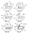
- a multilayer circuit board according to a third embodiment of the present invention is explained in detail below.
- this multilayer circuit board comprises a substrate 10 having a first surface 11 that is a horizontal surface, second surface 14 that is a horizontal surface extending at a different level from the first surface, and a third surface 16 extending in a substantially vertical direction between the first surface 11 and the second surface 14, and a multilayer circuit formed on the substrate 10, which is manufactured by alternately laminating a conductive layer (20, 22, 24, 26) and an insulation layer (30, 32, 34) on a required number of times.
- Each of the insulation layers (30, 32, 34) and the conductive layers (20, 22, 24, 26) can be formed by the same method as explained in the first embodiment.
- This embodiment is characterized in that a layer-to-layer connection of the multilayer circuit is made through a circuit pattern (21, 25) for layer-to-layer connection formed on a cutting surface (side surface) 19 of the substrate 10.
- the circuit pattern (21, 25) for layer-to-layer connection can be formed by the following procedure. That is, after the formation of the multilayer circuit on the substrate is finished, the substrate 10 with the multilayer circuit is cut in a substantially vertical direction such that a cutting surface of the multilayer circuit is flush with the cutting surface 19 of the substrate 10. As a result, connection ends (20a, 22a, 24a, 26a) of the conductive layers (20, 22, 24, 26) are exposed on the cutting surface 19. Circuit patterns (21, 25) for layer-to-layer connection are connected to those connection ends. As an example, a third conductive layer 24 having a circuit pattern and the connection end 24a on a second insulation layer 32 is shown in FIG. 13A. FIG.
- 13C is a cross-sectional view taken on the line I-I of FIG. 13A and the line II-II of FIG. 13B.
- one of the circuit patterns 25 extends from the connection end 20a to the connection end 26a through the cutting surface (side surface) 19 of the substrate 10
- the other one of the circuit patterns 21 extends from the connection end 22a to the connection end 24a through the cutting surface (side surface) 19 of the substrate 10.
- the connection ends (20a, 22a, 24a, 26a) when parts of the conductive layers other than the connection ends (20a, 22a, 24a, 26a) are exposed outside, it is preferred to form an insulation film 36 having windows 38 for the formation of layer-to-layer connection in predetermined positions on the cutting surface of the multilayer circuit, as shown in FIG. 14, and connect the connection ends with the circuit patterns (21, 23, 25) through these windows 38.
- the numeral 31 designates an additional insulation film formed at the point of intersection of the circuit patterns (21, 23) to make electrical insulation therebetween.
- a device-mounting portion 60 on which an electronic device(s) 70 such as IC chips can be mounted, may be formed on cutting surface 19 of the substrate 10, as shown in FIG. 15.
- the circuit patterns (21, 25) for layer-to-layer connection extend through the electronic device 70 mounted on this device-mounting portion 60.
- the cutting operation for the multilayer circuit board is not limited to the above embodiment.
- the cutting operation may be performed at a side of the second surface 14, as shown in FIG. 16A, or at only a corner of the second surface 14, as shown in FIG. 16B, or such that a through hole 80 having a required shape is formed in the second surface 14, as shown in FIG. 16C.
- an aperture 40 having a depth of reaching the second surface 14 of the substrate 10 is formed in the multilayer circuit, and a part of the substrate 10 is removed through the aperture 40 to form a concave 18 in the second surface 14, as shown in FIG. 17.
- an electronic device 70 such as IC chips can be mounted in the concave 18, and a circuit pattern 27 for layer-to-layer connection extends between the conductive layers (20, 24) through the electronic device 70 mounted in the concave 18.
- the concave 18 having the electronic device 70 and the aperture 40 may be filled with a sealing resin.
- an aperture 40 having the depth of reaching the second surface 14 of the substrate 10 is formed in the multilayer circuit, and a part of the substrate 10 is removed through the aperture 40 to obtain the concave 18 in the second surface 14.
- this modification is characterized in that exposed cutting surfaces of the multilayer circuit in the aperture 40 are inclined surfaces to improve the easiness of laser patterning.
- no electronic device is mounted in the concave 18, but a desired device can be mounted therein, if necessary.
- a layer-to-layer connection between the conductive layers (24, 26) is made by a circuit pattern 27 formed on the exposed cutting surface of the multilayer circuit.
- circuit pattern 29 formed on a bottom of the concave 18. Since the exposed cutting surface of the multilayer circuit is the inclined surface, these circuit patterns can be readily formed with precision by laser patterning.
- the multilayer circuit is cut.
- the cutting operation may be performed at a desired timing during the formation of the multilayer circuit. In this case, it is possible to carry out the formation of the conductive layer of the multilayer circuit simultaneously with the formation of the circuit pattern for layer-to-layer connection.
- each of the conductive layers and the insulation layers of the multilayer circuit is formed by means of film formation to achieve high integration of the multilayer circuit board.
- a plurality of layer-to-layer connections are formed on only the exposed cutting surface of the multilayer circuit having the reduced thickness, there is a fear that the reliability of the layer-to-layer connection deteriorates.
- the circuit pattern for layer-to-layer connection is formed so as to extend between the desired conductive layers of the multilayer circuit through the exposed cutting surface of the substrate, it is possible to avoid such a deterioration of the reliability of the layer-to-layer connection.
- the method of forming the conductive layer of the multilayer circuit can be also applied to form the circuit pattern for layer-to-layer connection, and problems peculiar to the formation of through-holes or via-holes can be avoided. Therefore, even when high-density wiring of the layer-to-layer connections is needed, it is possible to provide a high degree of flexibility in circuit design, without deteriorating the reliability of the layer-to-layer connections.
Abstract
Description
Claims (15)
- A multilayer circuit board comprising:a substrate (10) having a first surface (11, 14) and a second surface (12, 15, 19) extending from an end of the first surface at a required angle relative to the first surface;a multilayer circuit formed on the first surface of said substrate and composed of a plurality of circuit layers, each of which is provided with a conductive layer (20, 22, 24, 26) having a required circuit pattern and an insulation layer (30, 32, 34) formed on said conductive layer by film formation;a second conductive layer formed on the second surface (12, 15, 19) of said substrate, by which a layer-to-layer connection of said multilayer circuit is made.
- The multilayer circuit board as set forth in claim 1, wherein the second surface of said substrate (10) is a side surface (12, 15) of a projection (13, 17) on the first surface (11, 14).
- The multilayer circuit board as set forth in claim 1, wherein the first surface is a top surface (11, 14) of said substrate (10), and the second surface is a side surface (19) of said substrate.
- The multilayer circuit board as set forth in claim 1, wherein the required angle () between the first and second surfaces (14, 15) is an obtuse angle.
- The multilayer circuit board as set forth in claim 1, wherein said multilayer circuit has an aperture (40), through which a part of the first surface (14) is exposed, and an electronic device (70) is mounted in a concave (18) formed in the exposed first surface, and an electrical connection between said multilayer circuit and said electronic device is made by a third conductive layer (27) formed on an inner surface of said concave.
- The multilayer circuit board as set forth in claim 1, wherein said second conductive layer is a plurality of second conductive layers (21, 23) to obtain plural layer-to-layer connections of said multilayer circuit, and each of second conductive layers (21) is separated from an adjacent second conductive layer (23) in the thickness direction by a second insulation layer (31).
- The multilayer circuit board as set forth in claim 1, wherein said substrate (10) has a third surface (11) extending at a different level from the first surface (14) and a fourth surface (16) extending from the other end of the first surface to an end of the third surface, and said multilayer circuit is formed on the first, third and fourth surfaces of said substrate, and said second conductive layer is formed on a side surface (15) of a projection (17) on the first surface (14) to make the layer-to-layer connection of said multilayer circuit.
- A method of manufacturing a multilayer circuit board comprising the steps of:providing a substrate (10) having a first surface (11, 14) and a second surface (12, 15, 19) extending from an end of the first surface at a required angle relative to the first surface;performing a given number of circuit-layer forming steps to obtain a multilayer circuit on the first surface of said substrate, each of said circuit-layer forming steps including forming a conductive layer (20, 22, 24, 26) having a required pattern and forming an insulation layer (30, 32, 34) on said conductive layer by means of film formation;forming a second conductive layer on the second surface (12, 15, 19) of said substrate, by which a layer-to-layer connection of said multilayer circuit is made.
- The method as set forth in claim 8, wherein the first surface is a top surface (11, 14) of said substrate (10), and the second surface is a side surface (12, 15) of a projection (13, 17) on the first surface, and wherein said second conductive layer is formed on the side surface of said projection during said circuit-layer forming steps.
- The method as set forth in claim 8, wherein said second conductive layer is obtained by cutting said substrate (10) having said multilayer circuit such that a cutting surface of said multilayer circuit is flush with the cutting surface (19) of said substrate, and forming a conductive film (21, 23, 25) for layer-to-layer connection on the cutting surfaces of said multilayer circuit and said substrate.
- The method as set forth in claim 8, wherein said second conductive layer is obtained by forming a copper film on said second surface, and removing a required region of said copper film by use of a laser beam (50).
- The method as set forth in claim 8, wherein the first surface is a top surface (11, 14) of said substrate (10), and the second surface is a side surface (19) of said substrate, and wherein said second conductive layer is formed on the side surface.
- The method as set forth in claim 8, wherein said insulation layer (30, 32, 34) is formed by means of one of deposition polymerization and plasma polymerization.
- The method as set forth in claim 8, wherein said insulation layer (30, 32, 34) is obtained by forming a film of an insulating resin having photocurability on said conductive layer (20, 22, 24), and curing said film under light irradiation.
- The method as set forth in claim 8, wherein said insulation layer (30, 32, 34) is obtained by thermo-compression bonding a sheet of an insulating resin on said conductive layer (20, 22, 24).
Applications Claiming Priority (4)
| Application Number | Priority Date | Filing Date | Title |
|---|---|---|---|
| JP2000360220 | 2000-11-27 | ||
| JP2000360220A JP3888052B2 (en) | 2000-11-27 | 2000-11-27 | Multilayer three-dimensional circuit board and manufacturing method thereof |
| JP2000367091A JP2002171067A (en) | 2000-12-01 | 2000-12-01 | Multi-layered three-dimensional circuit board and its manufacturing method |
| JP2000367091 | 2000-12-01 |
Publications (2)
| Publication Number | Publication Date |
|---|---|
| EP1209959A2 true EP1209959A2 (en) | 2002-05-29 |
| EP1209959A3 EP1209959A3 (en) | 2004-03-10 |
Family
ID=26604663
Family Applications (1)
| Application Number | Title | Priority Date | Filing Date |
|---|---|---|---|
| EP01126948A Withdrawn EP1209959A3 (en) | 2000-11-27 | 2001-11-13 | Multilayer circuit board and method of manufacturing the same |
Country Status (5)
| Country | Link |
|---|---|
| US (1) | US6833511B2 (en) |
| EP (1) | EP1209959A3 (en) |
| KR (1) | KR100439593B1 (en) |
| CN (1) | CN1181718C (en) |
| TW (1) | TW507514B (en) |
Cited By (11)
| Publication number | Priority date | Publication date | Assignee | Title |
|---|---|---|---|---|
| US7189009B2 (en) | 2003-05-15 | 2007-03-13 | Infineon Technologies, Ag | Micro-optical module with housing and method for producing the same |
| DE102008003372A1 (en) | 2008-01-08 | 2009-07-16 | Otto-Von-Guericke-Universität Magdeburg | Two/three-dimensional multi-layer circuit carrier producing method for e.g. automobile industry, involves applying layer of strip conductor and dielectric layer on topmost dielectric layer alternatively |
| EP2141969A1 (en) * | 2008-07-04 | 2010-01-06 | Thales Nederland B.V. | A method for making a three-dimensional multi-layered interconnect device |
| US8033014B2 (en) | 2008-07-07 | 2011-10-11 | Unimicron Technology Corp. | Method of making a molded interconnect device |
| EP2469990A3 (en) * | 2008-04-30 | 2012-09-19 | Panasonic Corporation | Method of producing ciruit board by additive method, and circuit board and multilayer circuit board obtained by the method |
| US8436254B2 (en) | 2008-07-14 | 2013-05-07 | Unimicron Technology Corp. | Method of fabricating circuit board structure |
| US9082438B2 (en) | 2008-12-02 | 2015-07-14 | Panasonic Corporation | Three-dimensional structure for wiring formation |
| EP2825004A4 (en) * | 2012-03-06 | 2015-12-23 | Tyco Electronics Japan G K | Three-dimensional laminated wiring substrate |
| US9332650B2 (en) | 2008-04-30 | 2016-05-03 | Panasonic Corporation | Method of producing multilayer circuit board |
| US10039195B2 (en) | 2014-10-23 | 2018-07-31 | Facebook, Inc. | Fabrication of intra-structure conductive traces and interconnects for three-dimensional manufactured structures |
| US10099429B2 (en) | 2014-10-23 | 2018-10-16 | Facebook, Inc. | Methods for generating 3D printed substrates for electronics assembled in a modular fashion |
Families Citing this family (12)
| Publication number | Priority date | Publication date | Assignee | Title |
|---|---|---|---|---|
| EP2143310A1 (en) * | 2007-04-24 | 2010-01-13 | CeramTec AG | Method for the selective surface treatment of non-flat workpieces |
| CN101321154B (en) * | 2007-06-08 | 2012-06-06 | 华硕电脑股份有限公司 | Circuit board |
| KR100918490B1 (en) * | 2007-07-03 | 2009-09-24 | 주식회사 맥퀸트로닉 | Manufacturing method of zebra connector |
| EP2173147A4 (en) * | 2007-07-13 | 2012-10-31 | Ibiden Co Ltd | Wiring board and its manufacturing method |
| TWI394506B (en) * | 2008-10-13 | 2013-04-21 | Unimicron Technology Corp | Multilayer three-dimensional circuit structure and manufacturing method thereof |
| EP2619268A4 (en) * | 2010-09-23 | 2017-03-29 | Henkel IP & Holding GmbH | Chemical vapor resistant epoxy composition |
| WO2014125851A1 (en) * | 2013-02-14 | 2014-08-21 | 株式会社村田製作所 | Circuit substrate, and production method therefor |
| TWI561132B (en) | 2013-11-01 | 2016-12-01 | Ind Tech Res Inst | Method for forming metal circuit, liquid trigger material for forming metal circuit and metal circuit structure |
| US9590292B2 (en) | 2014-12-08 | 2017-03-07 | Industrial Technology Research Institute | Beam antenna |
| CN107404797B (en) * | 2016-05-18 | 2019-06-11 | 庆鼎精密电子(淮安)有限公司 | Multilayer circuit board and preparation method thereof with segment difference structure |
| CN106735922B (en) * | 2017-01-16 | 2018-10-09 | 深圳顺络电子股份有限公司 | A kind of laminate electronic components and preparation method thereof |
| CN112969277B (en) * | 2021-02-03 | 2023-03-14 | 深圳市同创鑫电子有限公司 | Multilayer circuit board and preparation method thereof |
Citations (2)
| Publication number | Priority date | Publication date | Assignee | Title |
|---|---|---|---|---|
| US3756891A (en) * | 1967-12-26 | 1973-09-04 | Multilayer circuit board techniques | |
| JPH06152098A (en) * | 1992-11-13 | 1994-05-31 | Fujitsu Ltd | Three-dimensional printed wiring molded object and its manufacture |
Family Cites Families (22)
| Publication number | Priority date | Publication date | Assignee | Title |
|---|---|---|---|---|
| DE1223908B (en) * | 1965-06-04 | 1966-09-01 | Siemens Ag | Electronic assembly consisting of electrical components cast in a plastic block, the connecting wires of which are connected to the surface of the plastic block, and a process for their production |
| US3349162A (en) * | 1965-08-23 | 1967-10-24 | Automatic Elect Lab | Intra-connection techniques for multilayer printed wiring boards |
| US4963697A (en) * | 1988-02-12 | 1990-10-16 | Texas Instruments Incorporated | Advanced polymers on metal printed wiring board |
| US5080455A (en) * | 1988-05-17 | 1992-01-14 | William James King | Ion beam sputter processing |
| ATE125666T1 (en) * | 1991-02-07 | 1995-08-15 | Siemens Ag | MICRO MULTILAYER WIRING. |
| US5164332A (en) * | 1991-03-15 | 1992-11-17 | Microelectronics And Computer Technology Corporation | Diffusion barrier for copper features |
| JPH0541580A (en) * | 1991-08-05 | 1993-02-19 | Nitto Denko Corp | Multilayer circuit board |
| JP2844584B2 (en) * | 1991-09-24 | 1999-01-06 | 日立電線株式会社 | Electromagnetically shielded circuit board |
| US5584120A (en) * | 1992-02-14 | 1996-12-17 | Research Organization For Circuit Knowledge | Method of manufacturing printed circuits |
| JP2889763B2 (en) * | 1992-05-29 | 1999-05-10 | 株式会社日立製作所 | Plastic molded housing with three-dimensional multilayer wiring and method of manufacturing the same |
| JPH07170077A (en) * | 1993-12-16 | 1995-07-04 | Hitachi Cable Ltd | Manufacture of injection-molded circuit part |
| JP3067515B2 (en) * | 1994-03-09 | 2000-07-17 | 日立電線株式会社 | Multilayer circuit molded body and method of manufacturing the same |
| FR2719967B1 (en) * | 1994-05-10 | 1996-06-07 | Thomson Csf | Three-dimensional interconnection of electronic component boxes using printed circuits. |
| JP3165605B2 (en) * | 1994-12-27 | 2001-05-14 | シャープ株式会社 | Manufacturing method of multilayer printed wiring board |
| JP3720846B2 (en) * | 1995-03-27 | 2005-11-30 | コーニンクレッカ フィリップス エレクトロニクス エヌ ヴィ | Method for manufacturing a plurality of electronic multilayer components |
| US5657537A (en) * | 1995-05-30 | 1997-08-19 | General Electric Company | Method for fabricating a stack of two dimensional circuit modules |
| JPH09153661A (en) * | 1995-12-01 | 1997-06-10 | Hitachi Chem Co Ltd | Wiring board and manufacture thereof |
| US6100178A (en) * | 1997-02-28 | 2000-08-08 | Ford Motor Company | Three-dimensional electronic circuit with multiple conductor layers and method for manufacturing same |
| JPH10282145A (en) * | 1997-04-02 | 1998-10-23 | Hoya Corp | Glass wiring board, method of manufacturing glass wiring board and probe card |
| US5956609A (en) * | 1997-08-11 | 1999-09-21 | Taiwan Semiconductor Manufacturing Company, Ltd. | Method for reducing stress and improving step-coverage of tungsten interconnects and plugs |
| KR100270869B1 (en) * | 1997-10-10 | 2001-01-15 | 윤종용 | Three dimensional composite cubic circuit board |
| US5903440A (en) * | 1998-01-30 | 1999-05-11 | Delco Electronics Corporaiton | Method of forming assemblies of circuit boards in different planes |
-
2001
- 2001-11-13 EP EP01126948A patent/EP1209959A3/en not_active Withdrawn
- 2001-11-13 TW TW090128064A patent/TW507514B/en not_active IP Right Cessation
- 2001-11-26 KR KR10-2001-0073721A patent/KR100439593B1/en not_active IP Right Cessation
- 2001-11-26 CN CNB011401311A patent/CN1181718C/en not_active Expired - Fee Related
- 2001-11-27 US US09/995,085 patent/US6833511B2/en not_active Expired - Fee Related
Patent Citations (2)
| Publication number | Priority date | Publication date | Assignee | Title |
|---|---|---|---|---|
| US3756891A (en) * | 1967-12-26 | 1973-09-04 | Multilayer circuit board techniques | |
| JPH06152098A (en) * | 1992-11-13 | 1994-05-31 | Fujitsu Ltd | Three-dimensional printed wiring molded object and its manufacture |
Cited By (12)
| Publication number | Priority date | Publication date | Assignee | Title |
|---|---|---|---|---|
| US7189009B2 (en) | 2003-05-15 | 2007-03-13 | Infineon Technologies, Ag | Micro-optical module with housing and method for producing the same |
| DE102008003372A1 (en) | 2008-01-08 | 2009-07-16 | Otto-Von-Guericke-Universität Magdeburg | Two/three-dimensional multi-layer circuit carrier producing method for e.g. automobile industry, involves applying layer of strip conductor and dielectric layer on topmost dielectric layer alternatively |
| EP2469990A3 (en) * | 2008-04-30 | 2012-09-19 | Panasonic Corporation | Method of producing ciruit board by additive method, and circuit board and multilayer circuit board obtained by the method |
| US9332650B2 (en) | 2008-04-30 | 2016-05-03 | Panasonic Corporation | Method of producing multilayer circuit board |
| EP2141969A1 (en) * | 2008-07-04 | 2010-01-06 | Thales Nederland B.V. | A method for making a three-dimensional multi-layered interconnect device |
| US8033014B2 (en) | 2008-07-07 | 2011-10-11 | Unimicron Technology Corp. | Method of making a molded interconnect device |
| US8436254B2 (en) | 2008-07-14 | 2013-05-07 | Unimicron Technology Corp. | Method of fabricating circuit board structure |
| US9082438B2 (en) | 2008-12-02 | 2015-07-14 | Panasonic Corporation | Three-dimensional structure for wiring formation |
| EP2825004A4 (en) * | 2012-03-06 | 2015-12-23 | Tyco Electronics Japan G K | Three-dimensional laminated wiring substrate |
| US9894758B2 (en) | 2012-03-06 | 2018-02-13 | Tyco Electronics Japan G.K. | Three-dimensional laminated wiring substrate |
| US10039195B2 (en) | 2014-10-23 | 2018-07-31 | Facebook, Inc. | Fabrication of intra-structure conductive traces and interconnects for three-dimensional manufactured structures |
| US10099429B2 (en) | 2014-10-23 | 2018-10-16 | Facebook, Inc. | Methods for generating 3D printed substrates for electronics assembled in a modular fashion |
Also Published As
| Publication number | Publication date |
|---|---|
| TW507514B (en) | 2002-10-21 |
| US20020062987A1 (en) | 2002-05-30 |
| CN1181718C (en) | 2004-12-22 |
| US6833511B2 (en) | 2004-12-21 |
| EP1209959A3 (en) | 2004-03-10 |
| KR20020041298A (en) | 2002-06-01 |
| KR100439593B1 (en) | 2004-07-12 |
| CN1356863A (en) | 2002-07-03 |
Similar Documents
| Publication | Publication Date | Title |
|---|---|---|
| US6833511B2 (en) | Multilayer circuit board and method of manufacturing the same | |
| US6783652B2 (en) | Process for manufacturing a wiring board | |
| KR101455234B1 (en) | Method for manufacturing a circuit board structure, and a circuit board structure | |
| KR101013325B1 (en) | Method for embedding a component in a base and forming a contact | |
| CN102111968B (en) | Method of manufacturing multilayer wiring substrate, and multilayer wiring substrate | |
| JP3629375B2 (en) | Multilayer circuit board manufacturing method | |
| US20100242272A1 (en) | Method of manufacturing printed circuit board | |
| CN212064497U (en) | Component carrier | |
| US10531577B1 (en) | Forming through holes through exposed dielectric material of component carrier | |
| EP3799540A1 (en) | Component carrier with through hole extending through multiple dielectric layers | |
| US8322596B2 (en) | Wiring substrate manufacturing method | |
| CA2387012C (en) | Method of manufacturing printed wiring board | |
| CN210928127U (en) | Component carrier | |
| KR20050072678A (en) | Multilayer interconnection board and production method thereof | |
| TWM599067U (en) | Low overhang component carrier with through hole having different front and back side window sizes | |
| KR100770168B1 (en) | Fabricating method for circuit board | |
| JP7397718B2 (en) | Printed wiring board and method for manufacturing printed wiring board | |
| JP7423326B2 (en) | Printed wiring board and method for manufacturing printed wiring board | |
| US20220285251A1 (en) | Semiconductor package substrate and method of manufacturing the same, and semiconductor package and method of manufacturing the same | |
| EP4250879A1 (en) | Inlay with exposed porous layer, component carrier and manufacture method | |
| JP7336845B2 (en) | Method for manufacturing printed wiring board | |
| KR100651568B1 (en) | Manufacturing method of chip embedded pcb using an engraved mold | |
| KR0149790B1 (en) | Board with an external port on one side and manufacturing method of the same package using the board and manufacturing method of the same | |
| KR100651323B1 (en) | Semiconductor package board having warpage resistant material layers | |
| TWM598520U (en) | Component carrier with bridge structure in through hole with reliability enhancing combination of parameters |
Legal Events
| Date | Code | Title | Description |
|---|---|---|---|
| PUAI | Public reference made under article 153(3) epc to a published international application that has entered the european phase |
Free format text: ORIGINAL CODE: 0009012 |
|
| AK | Designated contracting states |
Kind code of ref document: A2 Designated state(s): AT BE CH CY DE DK ES FI FR GB GR IE IT LI LU MC NL PT SE TR |
|
| AX | Request for extension of the european patent |
Free format text: AL;LT;LV;MK;RO;SI |
|
| PUAL | Search report despatched |
Free format text: ORIGINAL CODE: 0009013 |
|
| AK | Designated contracting states |
Kind code of ref document: A3 Designated state(s): AT BE CH CY DE DK ES FI FR GB GR IE IT LI LU MC NL PT SE TR |
|
| AX | Request for extension of the european patent |
Extension state: AL LT LV MK RO SI |
|
| 17P | Request for examination filed |
Effective date: 20040903 |
|
| AKX | Designation fees paid |
Designated state(s): AT BE CH CY DE DK ES FI FR GB GR IE IT LI LU MC NL PT SE TR |
|
| RAP1 | Party data changed (applicant data changed or rights of an application transferred) |
Owner name: PANASONIC ELECTRIC WORKS CO., LTD. |
|
| 17Q | First examination report despatched |
Effective date: 20090702 |
|
| GRAP | Despatch of communication of intention to grant a patent |
Free format text: ORIGINAL CODE: EPIDOSNIGR1 |
|
| STAA | Information on the status of an ep patent application or granted ep patent |
Free format text: STATUS: THE APPLICATION IS DEEMED TO BE WITHDRAWN |
|
| 18D | Application deemed to be withdrawn |
Effective date: 20110830 |