EP1209687A2 - A synthesizable synchronous static RAM - Google Patents
A synthesizable synchronous static RAM Download PDFInfo
- Publication number
- EP1209687A2 EP1209687A2 EP01127859A EP01127859A EP1209687A2 EP 1209687 A2 EP1209687 A2 EP 1209687A2 EP 01127859 A EP01127859 A EP 01127859A EP 01127859 A EP01127859 A EP 01127859A EP 1209687 A2 EP1209687 A2 EP 1209687A2
- Authority
- EP
- European Patent Office
- Prior art keywords
- custom
- synthesizable
- semi
- static ram
- synchronous static
- Prior art date
- Legal status (The legal status is an assumption and is not a legal conclusion. Google has not performed a legal analysis and makes no representation as to the accuracy of the status listed.)
- Withdrawn
Links
Images




Classifications
-
- G—PHYSICS
- G11—INFORMATION STORAGE
- G11C—STATIC STORES
- G11C11/00—Digital stores characterised by the use of particular electric or magnetic storage elements; Storage elements therefor
- G11C11/21—Digital stores characterised by the use of particular electric or magnetic storage elements; Storage elements therefor using electric elements
- G11C11/34—Digital stores characterised by the use of particular electric or magnetic storage elements; Storage elements therefor using electric elements using semiconductor devices
- G11C11/40—Digital stores characterised by the use of particular electric or magnetic storage elements; Storage elements therefor using electric elements using semiconductor devices using transistors
- G11C11/41—Digital stores characterised by the use of particular electric or magnetic storage elements; Storage elements therefor using electric elements using semiconductor devices using transistors forming static cells with positive feedback, i.e. cells not needing refreshing or charge regeneration, e.g. bistable multivibrator or Schmitt trigger
- G11C11/413—Auxiliary circuits, e.g. for addressing, decoding, driving, writing, sensing, timing or power reduction
- G11C11/417—Auxiliary circuits, e.g. for addressing, decoding, driving, writing, sensing, timing or power reduction for memory cells of the field-effect type
- G11C11/418—Address circuits
-
- G—PHYSICS
- G11—INFORMATION STORAGE
- G11C—STATIC STORES
- G11C11/00—Digital stores characterised by the use of particular electric or magnetic storage elements; Storage elements therefor
- G11C11/21—Digital stores characterised by the use of particular electric or magnetic storage elements; Storage elements therefor using electric elements
- G11C11/34—Digital stores characterised by the use of particular electric or magnetic storage elements; Storage elements therefor using electric elements using semiconductor devices
- G11C11/40—Digital stores characterised by the use of particular electric or magnetic storage elements; Storage elements therefor using electric elements using semiconductor devices using transistors
- G11C11/41—Digital stores characterised by the use of particular electric or magnetic storage elements; Storage elements therefor using electric elements using semiconductor devices using transistors forming static cells with positive feedback, i.e. cells not needing refreshing or charge regeneration, e.g. bistable multivibrator or Schmitt trigger
-
- G—PHYSICS
- G11—INFORMATION STORAGE
- G11C—STATIC STORES
- G11C11/00—Digital stores characterised by the use of particular electric or magnetic storage elements; Storage elements therefor
- G11C11/21—Digital stores characterised by the use of particular electric or magnetic storage elements; Storage elements therefor using electric elements
- G11C11/34—Digital stores characterised by the use of particular electric or magnetic storage elements; Storage elements therefor using electric elements using semiconductor devices
- G11C11/40—Digital stores characterised by the use of particular electric or magnetic storage elements; Storage elements therefor using electric elements using semiconductor devices using transistors
- G11C11/41—Digital stores characterised by the use of particular electric or magnetic storage elements; Storage elements therefor using electric elements using semiconductor devices using transistors forming static cells with positive feedback, i.e. cells not needing refreshing or charge regeneration, e.g. bistable multivibrator or Schmitt trigger
- G11C11/413—Auxiliary circuits, e.g. for addressing, decoding, driving, writing, sensing, timing or power reduction
- G11C11/417—Auxiliary circuits, e.g. for addressing, decoding, driving, writing, sensing, timing or power reduction for memory cells of the field-effect type
- G11C11/419—Read-write [R-W] circuits
Definitions
- This invention relates to a synthesizable, synchronous static RAM for use in ASICs.
- SRAM Static Random Access Memory
- SRAMs There are two types of SRAMs commonly in use:
- the operations inside the asynchronous memories are not synchronized to a clock, while in synchronous memories, all operations are synchronized to a clock signal.
- the SRAMs used in ASICs is optimized for high speed, low power, small areas and are synchronous in nature.
- the typical known synchronous SRAM contains a data input port, an address port, a clock, a memory select port, an output enable port, a write enable port and an output port [6].
- All the blocks mentioned above are made in the form of bit slice cells that are abutted to form a memory block of desired word x bit configuration.
- the memory development activity consists of making these leaf cells in a new technology and tuning them according to the full range of words and bits required.
- a critical path is used for the scheduling of various operations, which are triggered, by the positive edge of the external clock. This critical path is characterized on CAD tools to tune the memory for different shapes and sizes [1,5].
- There are self-timing structures which use a dummy path along the core and are triggered at the positive edge of the internal clocks (generated by the clock generation circuits). These structures are used to switch off the sense amps and intialize precharging at a suitable time (after the r/w operation has ended) [5]. This saves power consumption and decreases the cycle time of the memory [5].
- the object of this invention is to obviate the above drawbacks by providing a synthesizable synchronous static RAM using a combination of custom and semi-custom built blocks.
- the second object of this invention is to improve the speed of access of the synchronous static RAM.
- the third object of this invention is to provide easy testability.
- Another object of this invention is to provide asynchronous initialization.
- Yet, another object of this invention is to provide memory modeling at the RTL level.
- Further object of this invention is to enable automatic layout and thereby reduce the design time.
- this invention provides a synthesizable, synchronous static RAM comprising:
- the said custom-built memcells in bit slice are compatible with semi-custom synthesis tools and standard cell layout design rules for simulation and automatic layout thereby reducing design time.
- the said memcell and IO / precharge section in the said bit slice comprise a single column of memory cells connected to common bit lines.
- the said semi custom built decoder including flip-flops at its output for prevention of any glitches arising from reaching said custom-built bit memcells, said flip flops being driven by clock tree signals to reduce clock skew and address setup time thereby improving speed of operation.
- the said decoder is a fully synthesizable block for which an RTL is available.
- the said semi-custom decoder includes buffers so as to improve the speed of access.
- the said custom built memcells, semi-custom decoder and IO section and semi-custom clock generation circuitry are collectively and individually testable using RTL models for each unit.
- the said flip flops are provided with a common asynchronous preset / clear input so as to enable simultaneous selection of all word lines and thereby all memory locations, for writing common initialization values (the value at the said Data Input Port) at all memory locations.
- the said asynchronous preset / clear signal is used to provide means for asynchronous reset.
- the said flip- flop can be used to select multiple word lines simultaneously thus providing a synchronous initialization through SCAN inputs.
- the ODDON input means is used to provide a checker board test pattern initialization.
- the said RTL code is mapped over any technology library whether high speed low power low leakage.
- the said decoder is tested using Automatically generated test patterns by means of scan input.
- Figure 1 shows a typical single port SRAM in known art.
- Figure 2 shows the architecture of the synthesizable synchronous static RAM, according to this invention
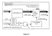
- FIG. 3 shows the architecture of the address decoder block, according to this invention.
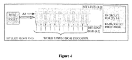
- Figure 4 shows the front-end structural model of the bit slice, according to this invention.
- Figure 5 shows the layout architecture of the bit slice core, according to this invention.
- Figure 6 shows the area comparison between classical memory and the 3SR RAM, according to this invention.
- FIG. 2 shows an SRAM according to this invention, which overcomes all the disadvantages of full custom SRAMs.
- the memory cells are full custom design organized as an array of bit slice sections (2.2).
- Address decoder (2.1) receives address signals (2.6) and clock signal (2.5) from external devices and generates word lines (2.8), clock-int (2.9) and OEN-int (2.10) to access the required memcell bit-slice section (2.2).
- Data input (2.4) received from external devices and Data Output (2.3) sent to external devices provide the data connection to the accessed memcell bit slice section (2.2).
- WEN (2.11) and OEN (2.12) are similarly connected to signals from external devices during write and read operations respectively.
- INITIALIZE (2.7) is an external signal used to initialize the bit-slice section (2.2) contents, with ODDON (2.13) being used for the special case of writing a "checkerboard" test pattern in the bit-slice section SCANPORTS (2.14) are standard scan-chain test signals for providing testability.
- the Address decoder (2.1) is a semi-custom built fully synthesizable block, for which an RTL code is written. The user can map the RTL code for the memory decoder in any of the technology library anytime like high speed low leakage low power.
- the custom-built memcell and a semi-custom IO precharge section in form of bit slice (2.2), semi-custom address decoder (2.1) and IO section (2.3 & 2.4) and semi custom clock generation circuitry (2.5) are collectively and individually testable using RTL models for each unit.
- This RTL code is compatible with DFT insertion tools.
- Figure 3 shows the internal structure of the semi-custom built address decoder (2.1), which decodes the address at the address ports (2.6) irrespective of the clock edge.
- the word lines generated at the output of Decoder (3.4) are latched in flip-flops (3.1) at the positive edge of the clock. This prevents any glitches arising at the output of Decoder (3.4) from reaching the custom-built memcells (2.2) shown in figure 2.
- the semi-custom built Address decoder (2.1) includes buffers (not shown) so as to increase the speed of access.
- the flip flops (3.1) are provided with inputs 'INITIALIZE' (2.7) and 'ODDON' (2.13) which control the asynchronous preset / clear inputs of the flip flops so as to enable simultaneous selection of all word lines or alternate word lines respectively and thereby implement writing of a common initialization value at all or alternate memory locations. This arrangement may be used to provide an asynchronous reset function.
- the clock (2.5) coming from the external devices is anded (3.5) with the output of CSN flip-flop (3.3) to reduce the power consumption when the memory has not been selected.
- a clock tree (3.2) is implemented for connecting the clock to all the flip-flops (3.1) in order to reduce the clock skew. This clock tree also takes care of the clock slope at all the flip-flop inputs.
- the clock tree feature is optional. Although the clock tree introduces some insertion delay in the clock path, which in turn adds to the access time of the memory it simultaneously reduces the address setup time. When the clock goes negative the word lines are deselected. For dual port or multiport SRAMs similar decoder architecture can be used for different ports.
- Each bit slice is a custom built single column of memory. It has two parts: Core and IO.
- Core contains the memory cells (2.2) and IO (2.3 & 2.4) contains the circuitry to write or read a data into or from a memory cell, selected by the respective word line, as well as for precharging the bit lines.
- the memory cells in bit slice (2.2) comprising of a single column of memory cells are connected to a common bit line (4.1) and common bit line bar (4.2). The individual columns are abutted in such a way as to form a single variable bit custom cell.
- Each memcell in bit slice form is connected to one of the word lines coming from the address decoder (2.1).
- the common bit line signal is finally connected to write and read circuitry (2.3, 2.4), which is made-up of standard cells like Flip-Flops, Nand, Nor, Latches, Tristate buffers, logic buffers, logic inverters, pull-ups etc.
- write and read circuitry (2.3, 2.4), which is made-up of standard cells like Flip-Flops, Nand, Nor, Latches, Tristate buffers, logic buffers, logic inverters, pull-ups etc.
- the physical layout of the memcells in bit slice form is shown in figure 5.
- the layouts of the custom built memcells and the gates in the IO circuitry of a single bit slice are kept abutted in such a way that they form a single variable width (depending upon the number of cells in one column) standard cell with the bit lines (4.1) running in metal 1 layer over memcells (2.2).
- the custom built memcells in bit slice form (2.2) are compatible with standard semi-custom simulation and synthesis tools so as to enable automatic layout thereby reducing design time.
- the height of each cell is equal to the height of the standard cell.
- VDD (5.1) and VSS (5.2) are put in such a metal layer in which they can connect directly to the standard cell power rail, without any metal via or filler cell.
- NWELL (5.4) and other standards for a standard cell are violated in such a way that all the violations are taken care of by a filler cell put at the end and the beginning of the bit slice core.
- Similar architectures can be made for dual port and multiport SRAM bit slices. Therefore, the bit slice is similar to a standard cell for layout purpose and can be placed anywhere with the other standard cells.
- the bit lines have been kept in a lower metal layer than the word lines (5.3) to shield them against any external signal.
- the user can run any signal in metal 2 layer but it should be in a perpendicular direction to the bit line direction, to decrease the coupling.
- the bit slice IO and the bit slice CORE are kept abutted by the Unix shell routines in the place & route tool environment
- the address decoder is synthesized and a full scan insertion [3,4] is done to make it testable. Thus, all the decoder faults can be detected through Automatic Test Program Generation (ATPG) techniques [3,4].
- the scan flip-flops at the word lines can be used to select more than one word line at a time (irrespective of the address at the address port). Thus, a desired pattern can be written in to the memory faster (decoding time is saved) and also in lesser clock cycles.
- the full memory can also be initialized through INITIALIZE and ODDON inputs.
- INITIALIZE also implements a synchronous (an asynchronous reset is also possible by using the Flip-Flops clear or preset pins directly) power on reset by selecting all the word lines in a single clock cycle.
- the data word at the data port of the bit slice is written to all the odd / even addresses, depending upon whether the ODDON pin is at logic 1/0.Thus in only two clock cycles one can create a checkerboard pattern inside the memory. Other patterns can also be written into the memory in the same way. This helps in detecting the Pattern Sensitive Faults (PSF) in the memory.
- PSF Pattern Sensitive Faults
- Figure 6 shows a size comparison between conventional full-custom memories and the 3SR architecture.
- the 3SR architecture shows an advantage for smaller configuration. In larger configurations the size penalty is only a maximum of 40%, which is very significantly less than for existing designs using semi-custom standard memcells.
- the area overhead is only a maximum of 40 %over a full custom design. This overhead can also be reduced if a high-density memory cell is used,
Landscapes
- Engineering & Computer Science (AREA)
- Microelectronics & Electronic Packaging (AREA)
- Computer Hardware Design (AREA)
- Static Random-Access Memory (AREA)
- For Increasing The Reliability Of Semiconductor Memories (AREA)
- Tests Of Electronic Circuits (AREA)
Abstract
Description
- synchronous
- asynchronous
- DECODER (1.1)
- CORE (1.2)
- IO section (1.3)
- Control and clock generation circuits (1.4)
- DUMMY Paths (not shown)
- the memory cells are full custom blocks that do not follow the standard cell design rules and hence cannot be placed along with the Standard Cells. They are therefore, treated as hard-core macros for which separate floor planning has to be done in the layout process resulting in a long time to get ready in a particular technology.
- the testability is poor as the standard design for testability (DFT) tools treat these custom cells as Black Boxes and hence do not model internal structure.
- there is no asynchronous reset facility, due to which these memories require a long time for initialization
- typically, these memories are routed in more than three metal layers. Hence, over-the-block routing in metal in higher levels is not possible.
- the Front End models in HDL's are behavioral owing to the custom design hence the modus operandi of the memory is not clear to the user. This makes debugging of these memories difficult.
- custom built memcells and a semi-custom IO / precharge section in form of bit slice,
- a semi-custom built decoder connected to said bit slice,
- a semi-custom built control clock generation section, which is connected to said semi-custom built decoder and IO section,
Claims (13)
- A synthesizable, synchronous static RAM comprising:the arrangement being such as to provides high speed access, easy testability and asynchronous initialization capabilities while reducing design time in a size that is significantly smaller than existing semi custom or standard cell base memory design.custom built memcells and a semi-custom IO / precharge section in form of bit slice,a semi-custom built decoder connected to said bit slice,a semi-custom built control clock generation section, which is connected to said semi-custom built decoder and IO section,
- A synthesizable, synchronous static RAM as claimed in claim 1 wherein said custom-built memcells in bit slice are compatible with semi-custom synthesis tools and standard cell layout design rules for simulation and automatic layout thereby reducing design time.
- A synthesizable, synchronous static RAM as claimed in claim 1 wherein said memcell and IO / precharge section in the said bit slice comprise a single column of memory cells connected to common bit lines.
- A synthesizable, synchronous static RAM as claimed in claim 1, wherein said semi custom built decoder including flip-flops at its output for prevention of any glitches arising from reaching said custom-built bit memcells, said flip flops being driven by clock tree signals to reduce clock skew and address setup time thereby improving speed of operation.
- A synthesizable, synchronous static RAM as claimed in claim 1 wherein the said decoder is a fully synthesizable block for which an RTL is available.
- A synthesizable, synchronous static RAM as claimed in claim 1, wherein said semi-custom decoder includes buffers so as to improve the speed of access.
- A synthesizable, synchronous static RAM as claimed in claim 1, wherein said custom built memcells, semi-custom decoder and IO section and semi-custom clock generation circuitry are collectively and individually testable using RTL models for each unit.
- A synthesizable, synchronous static RAM as claimed in claim 4, wherein said flip flops are provided with a common asynchronous preset / clear input so as to enable simultaneous selection of all word lines and thereby all memory locations, for writing common initialization values (the value at the said Data Input Port) at all memory locations.
- A synthesizable, synchronous static RAM as claimed in claim 8, wherein said asynchronous preset / clear signal is used to provide means for asynchronous reset.
- A synthesizable, synchronous static RAM as claimed in claim 8, wherein said flip- flop can be used to select multiple word lines simultaneously thus providing a synchronous initialization through SCAN inputs.
- A synthesizable, synchronous static RAM as claimed in claim 8, wherein ODDON input means is used to provide a checker board test pattern initialization.
- A synthesizable, synchronous static RAM as claimed in claim 5, wherein said RTL code is mapped over any technology library whether high speed low power low leakage.
- A synthesizable, synchronous static RAM as claimed in claim 1, wherein said decoder is tested using Automatically generated test patterns by means of scan input.
Applications Claiming Priority (2)
| Application Number | Priority Date | Filing Date | Title |
|---|---|---|---|
| IN1050DE2000 | 2000-11-23 | ||
| INDE105000 | 2000-11-23 |
Publications (2)
| Publication Number | Publication Date |
|---|---|
| EP1209687A2 true EP1209687A2 (en) | 2002-05-29 |
| EP1209687A3 EP1209687A3 (en) | 2002-09-18 |
Family
ID=11097125
Family Applications (1)
| Application Number | Title | Priority Date | Filing Date |
|---|---|---|---|
| EP01127859A Withdrawn EP1209687A3 (en) | 2000-11-23 | 2001-11-22 | A synthesizable synchronous static RAM |
Country Status (2)
| Country | Link |
|---|---|
| US (1) | US6470475B2 (en) |
| EP (1) | EP1209687A3 (en) |
Families Citing this family (13)
| Publication number | Priority date | Publication date | Assignee | Title |
|---|---|---|---|---|
| US6742169B2 (en) * | 2001-02-28 | 2004-05-25 | Sanyo Electric Co., Ltd. | Semiconductor device |
| US6957403B2 (en) | 2001-03-30 | 2005-10-18 | Syntest Technologies, Inc. | Computer-aided design system to automate scan synthesis at register-transfer level |
| US20030208738A1 (en) * | 2002-04-24 | 2003-11-06 | Yu-Ming Hsu | Design method for full chip element on memory |
| US7149916B1 (en) * | 2003-03-17 | 2006-12-12 | Network Equipment Technologies, Inc. | Method for time-domain synchronization across a bit-sliced data path design |
| JP2006303108A (en) * | 2005-04-19 | 2006-11-02 | Toshiba Corp | Semiconductor integrated circuit |
| EP1727156B1 (en) | 2005-05-18 | 2015-01-07 | STMicroelectronics Pvt. Ltd. | An improved area efficient memory architecture with decoder self test and debug capability |
| US7512908B2 (en) * | 2006-06-09 | 2009-03-31 | International Business Machines Corporation | Method and apparatus for improving SRAM cell stability by using boosted word lines |
| US7376042B2 (en) * | 2006-07-25 | 2008-05-20 | Qimonda Ag | Boosted clock circuit for semiconductor memory |
| US8516408B2 (en) * | 2009-05-26 | 2013-08-20 | Lsi Corporation | Optimization of circuits having repeatable circuit instances |
| US9058860B2 (en) * | 2012-03-29 | 2015-06-16 | Memoir Systems, Inc. | Methods and apparatus for synthesizing multi-port memory circuits |
| US8645893B1 (en) * | 2012-10-23 | 2014-02-04 | Arm Limited | Method of generating a layout of an integrated circuit comprising both standard cells and at least one memory instance |
| CN106291337B (en) * | 2016-07-25 | 2020-01-07 | 瑞萨集成电路设计(北京)有限公司 | Device and method for adjusting chip mode in scan chain test |
| EP3938943A1 (en) * | 2019-03-14 | 2022-01-19 | Xenergic AB | Method for implementing an integrated circuit comprising a random-access memory-in-logic |
Family Cites Families (6)
| Publication number | Priority date | Publication date | Assignee | Title |
|---|---|---|---|---|
| US4724531A (en) * | 1984-07-18 | 1988-02-09 | Hughes Aircraft Company | Gate array with bidirectional symmetry |
| JPS63237436A (en) * | 1987-03-26 | 1988-10-03 | Toshiba Corp | Wiring of semiconductor integrated circuit device |
| US5867399A (en) * | 1990-04-06 | 1999-02-02 | Lsi Logic Corporation | System and method for creating and validating structural description of electronic system from higher-level and behavior-oriented description |
| US5963454A (en) * | 1996-09-25 | 1999-10-05 | Vlsi Technology, Inc. | Method and apparatus for efficiently implementing complex function blocks in integrated circuit designs |
| JP2859234B2 (en) * | 1996-12-26 | 1999-02-17 | 日本電気アイシーマイコンシステム株式会社 | Semiconductor integrated circuit device |
| US6295627B1 (en) * | 1998-12-04 | 2001-09-25 | Cypress Semiconductor Corporation | Method and apparatus for the automated design of memory devices |
-
2001
- 2001-11-20 US US09/988,882 patent/US6470475B2/en not_active Expired - Lifetime
- 2001-11-22 EP EP01127859A patent/EP1209687A3/en not_active Withdrawn
Also Published As
| Publication number | Publication date |
|---|---|
| US6470475B2 (en) | 2002-10-22 |
| EP1209687A3 (en) | 2002-09-18 |
| US20020110042A1 (en) | 2002-08-15 |
Similar Documents
| Publication | Publication Date | Title |
|---|---|---|
| US6049487A (en) | Embedded static random access memory for field programmable gate array | |
| US5471428A (en) | High performance single port RAM generator architecture | |
| US7668035B2 (en) | Memory circuits with reduced leakage power and design structures for same | |
| US6470475B2 (en) | Synthesizable synchronous static RAM | |
| US7751266B2 (en) | High performance read bypass test for SRAM circuits | |
| US9947419B1 (en) | Apparatus and method for implementing design for testability (DFT) for bitline drivers of memory circuits | |
| US6370078B1 (en) | Way to compensate the effect of coupling between bitlines in a multi-port memories | |
| US6233197B1 (en) | Multi-port semiconductor memory and compiler having capacitance compensation | |
| Mohammad | Embedded Memory Design for Multi-Core and Systems on Chip | |
| Silburt et al. | A 180 MHz 0.8 mu m BiCMOS modular memory family of DRAM and multiport SRAM | |
| US5995425A (en) | Design of provably correct storage arrays | |
| Schmitt-Landsiedel et al. | Pipelined architecture for fast CMOS buffer RAMs | |
| US8824196B2 (en) | Single cycle data copy for two-port SRAM | |
| Nichols et al. | Automated synthesis of multi-port memories and control | |
| Mohammad | Embedded memory interface logic and interconnect testing | |
| Kushiyama et al. | An experimental 295 MHz CMOS 4K/spl times/256 SRAM using bidirectional read/write shared sense amps and self-timed pulsed word-line drivers | |
| US7242633B1 (en) | Memory device and method of transferring data in memory device | |
| US7248491B1 (en) | Circuit for and method of implementing a content addressable memory in a programmable logic device | |
| JP4471582B2 (en) | Semiconductor integrated circuit and circuit design apparatus | |
| TW202324409A (en) | Power supply tracking circuitry for embedded memories | |
| Franch et al. | A 640-ps, 0.25-/spl mu/m CMOS, 16/spl times/64-b three-port register file | |
| US12045553B2 (en) | Method for implementing an integrated circuit comprising a random-access memory-in-logic | |
| US20260004842A1 (en) | Circuit for multiport register file | |
| Silburt et al. | A 200MHz 0.8 m BiCMOS modular memory family of DRAM and multi-port SRAM’s | |
| US20260038587A1 (en) | Clocking scheme for multi-port register file |
Legal Events
| Date | Code | Title | Description |
|---|---|---|---|
| PUAI | Public reference made under article 153(3) epc to a published international application that has entered the european phase |
Free format text: ORIGINAL CODE: 0009012 |
|
| AK | Designated contracting states |
Kind code of ref document: A2 Designated state(s): AT BE CH CY DE DK ES FI FR GB GR IE IT LI LU MC NL PT SE TR |
|
| AX | Request for extension of the european patent |
Free format text: AL;LT;LV;MK;RO;SI |
|
| PUAL | Search report despatched |
Free format text: ORIGINAL CODE: 0009013 |
|
| AK | Designated contracting states |
Kind code of ref document: A3 Designated state(s): AT BE CH CY DE DK ES FI FR GB GR IE IT LI LU MC NL PT SE TR |
|
| AX | Request for extension of the european patent |
Free format text: AL;LT;LV;MK;RO;SI |
|
| RIC1 | Information provided on ipc code assigned before grant |
Free format text: 7G 11C 11/41 A, 7G 11C 11/418 B, 7G 11C 11/419 B, 7G 06F 17/50 B |
|
| 17P | Request for examination filed |
Effective date: 20030314 |
|
| AKX | Designation fees paid |
Designated state(s): DE FR GB IT |
|
| 17Q | First examination report despatched |
Effective date: 20061213 |
|
| GRAP | Despatch of communication of intention to grant a patent |
Free format text: ORIGINAL CODE: EPIDOSNIGR1 |
|
| RAP1 | Party data changed (applicant data changed or rights of an application transferred) |
Owner name: STMICROELECTRONICS PVT. LTD. |
|
| STAA | Information on the status of an ep patent application or granted ep patent |
Free format text: STATUS: THE APPLICATION HAS BEEN WITHDRAWN |
|
| 18W | Application withdrawn |
Effective date: 20080728 |