EP1209677A1 - Noise compensation device and method in a discrete time control system - Google Patents
Noise compensation device and method in a discrete time control system Download PDFInfo
- Publication number
- EP1209677A1 EP1209677A1 EP00830776A EP00830776A EP1209677A1 EP 1209677 A1 EP1209677 A1 EP 1209677A1 EP 00830776 A EP00830776 A EP 00830776A EP 00830776 A EP00830776 A EP 00830776A EP 1209677 A1 EP1209677 A1 EP 1209677A1
- Authority
- EP
- European Patent Office
- Prior art keywords
- signal
- frequency
- timing signal
- timing
- generating
- Prior art date
- Legal status (The legal status is an assumption and is not a legal conclusion. Google has not performed a legal analysis and makes no representation as to the accuracy of the status listed.)
- Withdrawn
Links
Images


Classifications
-
- G—PHYSICS
- G11—INFORMATION STORAGE
- G11B—INFORMATION STORAGE BASED ON RELATIVE MOVEMENT BETWEEN RECORD CARRIER AND TRANSDUCER
- G11B20/00—Signal processing not specific to the method of recording or reproducing; Circuits therefor
- G11B20/10—Digital recording or reproducing
- G11B20/10009—Improvement or modification of read or write signals
-
- G—PHYSICS
- G11—INFORMATION STORAGE
- G11B—INFORMATION STORAGE BASED ON RELATIVE MOVEMENT BETWEEN RECORD CARRIER AND TRANSDUCER
- G11B20/00—Signal processing not specific to the method of recording or reproducing; Circuits therefor
- G11B20/24—Signal processing not specific to the method of recording or reproducing; Circuits therefor for reducing noise
Definitions
- the present invention refers to a noise compensation device and method in a discrete time control system.
- R/W devices referred to as hard disk drives (HDDs)
- HDDs hard disk drives
- the head-actuator assembly comprises a plurality of arms turning about a same rotation axis, integral with one another and actuated by a motor, and reading heads, each reading head being carried by a respective arm and facing respective surfaces of the disks.
- Control information is stored in preset control sectors on the disks, is picked up by the heads and enables detection of the position of the heads with respect to the tracks on the magnetic disks.
- the heads generate an analog signal that is sampled at a preset rate (depending upon the rotation rate of the disk) to generate a numeric position signal.
- the electronic control unit detects a position error on the basis of the numeric position signal and generates a numeric control signal for controlling the head-actuator assembly and keeping the heads in optimal reading positions.
- control system comprises an open loop compensation line for compensating the effects of external disturbance.
- an acceleration sensor for example, a sensor made using MicroElectroMechanicalSystem -MEMS- technology
- an acceleration sensor mounted so as to be integral with the casing of the R/W device, detects any disturbance mechanical vibration and supplies an acceleration signal which is, in turn, sampled at a compensation rate and used by the electronic control unit to generate a numeric compensation signal to be added to the control signal.
- the data supplied by the sensor and the control signal are not, however, synchronous, and thus cannot be immediately summed.
- synchronization techniques normally used carry out a sampling rate conversion.
- the sequence of data supplied by the sensor is initially expanded by interposing, between two consecutive samples, a first preset integer number L of null samples corresponding to instants comprised within a same sampling interval.
- the expanded sequence of data is then filtered using a low pass filter to replace the null samples with interpolated samples.
- a decimator reduces the expanded sequence of data, maintaining one sample every M samples (where M is a second preset integer number) and eliminating all the others.
- the aim of the present invention is to overcome the drawbacks of known devices.
- a noise compensating device and method in a discrete time control system as claimed in Claims 1 and 17, respectively.
- the invention is applied to a R/W device for hard disks, even though the invention may be applied to a generic discrete time control system with open loop noise compensation.
- an R/W device 1 for hard disks is housed inside a casing 2 and comprises a plurality of magnetic disks 7, a head-actuator assembly 4, and a control card 5.
- the magnetic disks 7 are mounted coaxially and rotationally integral to a shaft 8 of a motor (not shown) and have each a top surface 7a and a bottom surface 7b.
- control information is stored, in a per se known manner, in preset sectors of the magnetic disks 7.
- the head-actuator assembly 4 comprises a rotating support 13 (generally referred to as an E-block on account of its shape), a plurality of suspension arms 11, integrally connected to the rotating support 13, and a plurality of R/W heads 12 carried by respective suspension arms 11; in use, each head 12 faces a respective surface 7a, 7b of the magnetic disks 7, for reading and writing.
- a motor 14 is connected to and actuates the rotating support 13 for positioning the R/W heads 12 on a desired data track 15.
- the control card 5 is carried by the casing 2 and comprises a control unit 16 and a sensor assembly 17.
- the control card 5 is connected to the motor 14 through a connector of a known type (not shown).
- control unit 16 comprises a logic unit 20, a controller 21, a compensation block 22, a subtracting node 23, and an adding node 24.
- the logic unit 20 generates, in a known way, a reference signal S REF indicative of a target position for the read heads 12.
- the subtracting node 23 receives the reference signal S REF , as well as a position signal S POS issued on a first output of the head-actuator assembly 4, in a known way.
- the output of the subtracting node 23 is connected to an input of the controller 21.
- the controller 21 has an output connected to the adding node 24 and supplying a control signal S CONTR .
- the head-actuator assembly 4 has an input that is connected to the adding node 24 and a second output that is connected to the sensor assembly 17 and supplies a first timing signal T 1 .
- the control signal S CONTR and the first timing signal T 1 have a first frequency F 1 determined by the rotation rate of the disks 7 and by the number of control sectors present. For instance, in a disk having an angular speed of 5400 rpm and 60 control sectors, the first frequency F 1 is 5400 Hz.
- the sensor assembly 17 which will be described in detail later on with reference to Figure 4 and is preferably made in a single integrated device, has an output connected to an input of the compensation block 22.
- the sensor assembly 17 supplies, on its own output, an acceleration signal S ACC synchronized with the control signal S CONTR and representative of an acceleration A due to noise forces, such as mechanical vibrations, acting on the R/W device 1.
- the compensation block 22 has an output connected to the adding node 24 and supplying a compensation signal S COMP .
- the senor assembly 17 and the compensation block 22 form an open loop compensation line 27. Furthermore, the controller 21, the head-actuator assembly 4, the subtracting node 23 and adding node 24 form a control loop 25.
- the position signal S POS supplied by the head-actuator assembly 4 is representative of the distance of the read heads 12 from a center-of-track position and is generated when the read heads 12 fly on the sectors of the magnetic disks 7 storing the control information.
- the signal S POS is obtained, in a known way, by sampling an analog signal at the first frequency F 1 .
- the error signal S ERR and the control signal S CONTR generated within the control loop 25 are synchronous with the position signal S POS , and hence have the first frequency F 1 .
- the subtracting node 23 subtracts the position signal S POS from the reference signal S REF and generates an error signal S ERR .
- the error signal S ERR is then used in the controller 21 to obtain the control signal S CONTR , using any one of known control techniques (for example, a PID control technique).
- the adding node 24 receives the control signal S CONTR and the compensation signal S COMP (which are synchronized with one another) and adds them, to generate an actuation signal S ATT supplied to the head-actuator assembly 4 to correct the position of the read heads 12.
- the sensor assembly 17 comprises a sensing element 30, an acquisition stage 31, a synchronization stage 32, and an interface circuit 35.
- the acquisition stage 31 is connected between the sensing element 30 and the interface 35, and comprises an analog-to-digital converter 37, preferably of the sigma-delta type, a decimator 38, a numeric filter 39, a correction block 40, and an output register 41, cascade-connected together.
- the A/D converter 37 has a control output 37d connected to a control input of the sensing element 30.
- the sensing element 30 and the A/D converter 37 form an acquisition loop of the sigma-delta type, in itself known and described, for example, in M. Lemkin and B. Boser, "A Three Axis Micromachined Accelerometer with a CMOS Position-Sense Interface and Digital Offset-Trim Electronics", IEEE Journal of Solid State Circuits, Vol. 34, No. 4.
- the synchronization stage 32 comprises a phase locked loop (PLL) 42 and a phase generator circuit 43.
- the PLL 42 has an input 42a receiving the first timing signal T 1 , a first output 42b connected to a first input 37a of the A/D converter 37 and supplying a second timing signal T 2 , and a second output 42c connected to the timing input 38a of the decimator 38 and to a timing input 39b of the numeric filter 39 and supplying a third timing signal T 3 .
- the second timing signal T 2 and the third timing signal T 3 are generated as described below, starting from the first timing signal T 1 .
- the phase generator circuit 43 has inputs 43a and 43b receiving the first timing signal T 1 and, respectively, the third timing signal T 3 , and an output 43c connected to a decimation input 38b of the decimator 38 and to an activation input 39c of the numeric filter 39.
- the output 43c of the phase generator circuit 43 supplies decimation pulses T DEC at the first frequency F 1 and with a preset delay with respect to the first timing signal T 1 .
- the second timing signal T 2 has a second frequency F 2 not lower than the first frequency F 1
- the third timing signal T 3 has a third frequency F 3 comprised between the second frequency F 2 and the first frequency F 1 .
- F 2 M*F 1
- F 3 N*F 1
- the decimation pulses T DEC have the first frequency F 1 of the control signal S CONTR .
- the PLL 42 locks to the first timing signal T 1 of the control loop 25 and generates the second timing signal T 2 and the third timing signal T 3 .
- the phase generator circuit 43 generates decimation pulses T DEC with a preset delay K with respect to the edges of the first timing signal T 1 .
- the delay K is representative of the sample to be selected by the decimator 38.
- the A/D converter 37 receives, on a second input 37b, the analog measure signal V M and, using the second timing signal T 2 as internal timing signal, issues, on an output 37c, a sampled signal BS formed by a flow of bits oversampled with respect to the first frequency F 1 .
- the A/D converter 37 is of the sigma-delta type, the individual bits of the sampled signal BS are produced by the A/D converter 37 at the third frequency F 3 .
- the decimator 38 filters the sampled signal BS received from the A/D converter 37 in order to reconstruct an oversampled numeric signal, wherein every sample includes a preset number of bits, and in order to eliminate any high frequency components introduced by the analog measure signal V M . Indeed, if these component are not eliminated, decimation would cause a spectrum folding that, as known, causes distortions.
- the decimator 38 selects and supplies a sample to a data input 39a of the numeric filter 39, while the other samples are eliminated.
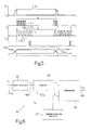
- the K-th sample following the rising edge of the first timing signal T 1 is selected, as illustrated in Figure 5, where the delay K is an integer number comprised between 0 and N - 1. Since a decimation pulse T DEC is generated at each cycle of the first timing signal T 1 , the decimator 38 outputs samples that have the same frequency F 1 as the first timing signal T 1 of the control loop 25.
- the numeric filter 39 which is preferably a second order self-regression filter (or infinite impulse response IIR filter) of a known type, filters the data received from the decimator 38 to eliminate the high frequency noise components and carry out a phase equalization in the frequency band of interest (for example, from 0 Hz to 800 Hz). This enables the phase delay introduced by the decimator 38 to be compensated and reduced to the minimum.
- a second order self-regression filter or infinite impulse response IIR filter
- the correction block 40 compensates the presence of offsets and the gain losses introduced by the acquisition stage 31 by adding an offset term to the samples received and, respectively, by multiplying the samples by a preset gain factor.
- the signal at the output of the correction block 40 is the acceleration signal S' ACC , which is stored in the FIFO type output register 41 to be read preferably in an immediately successive cycle of the first timing signal T 1 .
- each sample of the acceleration signal S ACC is representative of the acceleration detected by the sensing element 30 during the cycle that precedes the first timing signal T 1 and is made available through the interface 35 to be used by the compensation block 22 from the start of a cycle that immediately follows (as represented by the arrow in Figure 5).
- the acceleration signal S ACC has the first frequency F 1 and is therefore synchronous with the signals present in the control loop 25 (in particular, it is synchronous with the control signal S CONTR ).
- the phase generator circuit 43 comprises an edge detector 45, a counter 46, a synchronization register 47, and a comparator 48.
- the edge detector 45 is connected to the first input 43a of the phase generator circuit 43 (fed with the first timing signal T 1 ) and supplies reset pulses R at rising edges of the first timing signal T 1 .
- the counter 46 has a reset input 46a receiving the reset pulses R, is connected to the second input 43b of the phase generator circuit 43 (fed with the third timing signal T 3 ) and has an output supplying a counting signal C which is incremented at each cycle of the third timing signal T 3 and hence has the third frequency F 3 .
- the comparator 48 has a first input connected to the output of the counter 46, and a second input connected to an output of the synchronization register 42, which supplies the delay K.
- an output 43c of the comparator 48 switches, supplying a decimation pulse T DEC .
- the delay K is my be programmed by writing the synchronization register 47.
- the present noise compensating device generates a sampled signal BS having a frequency correlated to the signals present in the control loop 25.
- an acceleration signal S ACC may be generated, which represents accelerations due to disturbance forces acting on the R/W device 1 and is synchronous with the control signal S CONTR , without need of sampling frequency conversions.
- the samples of the acceleration signal S ACC may be generated immediately before being used by the compensation block 22.
- the phase of the compensation signal S COMP is not degraded. Rather, the use of the numeric filter 39 to perform an equalization, enables minimization of the phase delay, and thus ensures a high effectiveness of the open loop noise compensation.
- Synchronization is moreover performed using a hardware circuit instead of a firmware procedure.
- the design phase is thus simplified, and it is possible to reduce both the size of the nonvolatile memory storing the firmware and the required processing power.
- the numeric filter 39 eliminates of any noise outside of the frequency band, and in particular high frequency noise. Furthermore, the fact that the sensor assembly 17 is represented by a single integrated device means that the noise affecting the acceleration signal S ACC is very contained.
- the invention may be advantageously applied in all cases in which it is necessary to perform high precision open loop compensation in a discrete time control system.
- the numeric filter 39 may be of a programmable type and may be modified at any moment through the interface circuit 35. In this way, it is more versatile and is suitable for creating adaptive control systems.
- the sensor element may be of a different type and may comprise, for instance, one or more linear MEMS sensors. In this latter case, the sensors may be oriented along different axes in such a way as to detect different acceleration components. The signals supplied by each sensor may then be combined in a per se known manner for calculating the overall acceleration to which the R/W device 1 is subjected as a result of the disturbance forces.
Landscapes
- Engineering & Computer Science (AREA)
- Signal Processing (AREA)
- Soundproofing, Sound Blocking, And Sound Damping (AREA)
Abstract
A noise compensating device in a discrete time control system, for a R/W system for hard disks, including: a control loop (21-24) generating a first timing signal (T1), a signal indicative of a quantity to be controlled (SPOS), and a control signal (SCONTR), which have a first frequency (F1) ; and an open loop control line (27) which generates a compensation signal (SCOMP) synchronous with the control signal (SCONTR) and includes a sensor (17). The sensor includes a sensing element (30), generating an analog signal (VM), an acquisition stage (31), connected to the sensing element (30) and generating a disturbance measure signal (SACC) correlated to the analog signal (VM) and synchronous with the control signal (SCONTR), and a synchronization stage (32). The synchronization stage (32) includes a frequency generator (42) having an input receiving the first timing signal (T1) and a first and a second output (42b, 42c) connected to the acquisition stage (31) and generating, respectively, a second timing signal (T2) and a third timing signal (T3). <IMAGE> <IMAGE>
Description
The present invention refers to a noise compensation device
and method in a discrete time control system.
It is known that high precision control devices frequently
have, in addition to a feedback control system, closed loop
systems for compensating external noise. These compensation
systems use sensors detecting the presence of external noise
and generating compensation signals that are added to the
control signals used in the feedback loop.
In particular, discrete time control systems are required to
synchronize the control signals and the compensation signals
so that they may be correctly added.
An application of this compensation technique, to which
reference will be made hereinafter, are hard disk read/write
devices for controlling the position of reading heads.
As is known, R/W devices, referred to as hard disk drives
(HDDs), normally comprise a set of magnetic disks, rotating
all together, a head-actuator assembly, and an electronic
control unit. The head-actuator assembly comprises a
plurality of arms turning about a same rotation axis,
integral with one another and actuated by a motor, and
reading heads, each reading head being carried by a
respective arm and facing respective surfaces of the disks.
Control information is stored in preset control sectors on
the disks, is picked up by the heads and enables detection
of the position of the heads with respect to the tracks on
the magnetic disks. In particular, the heads generate an
analog signal that is sampled at a preset rate (depending
upon the rotation rate of the disk) to generate a numeric
position signal. The electronic control unit detects a
position error on the basis of the numeric position signal
and generates a numeric control signal for controlling the
head-actuator assembly and keeping the heads in optimal
reading positions.
In addition, the control system comprises an open loop
compensation line for compensating the effects of external
disturbance. In particular, an acceleration sensor (for
example, a sensor made using MicroElectroMechanicalSystem
-MEMS- technology), mounted so as to be integral with the
casing of the R/W device, detects any disturbance mechanical
vibration and supplies an acceleration signal which is, in
turn, sampled at a compensation rate and used by the
electronic control unit to generate a numeric compensation
signal to be added to the control signal.
The data supplied by the sensor and the control signal are
not, however, synchronous, and thus cannot be immediately
summed. To overcome this problem, synchronization techniques
normally used carry out a sampling rate conversion.
In practice, the sequence of data supplied by the sensor is
initially expanded by interposing, between two consecutive
samples, a first preset integer number L of null samples
corresponding to instants comprised within a same sampling
interval. The expanded sequence of data is then filtered
using a low pass filter to replace the null samples with
interpolated samples. Next, a decimator reduces the expanded
sequence of data, maintaining one sample every M samples
(where M is a second preset integer number) and eliminating
all the others. By selecting the numbers L and M so that the
condition
Fc = L + 1 M Fs
is satisfied, wherein Fc is the control sampling rate and Fs
is the sensor sampling rate, the sequence of data at the
output of the decimator is synchronous with the control
signal and can thus be used to generate the compensation
signal.
Known devices, however, have a number of drawbacks. In fact,
performing frequency conversions increases the phase delay
of the compensation signal with respect to the control
signal. This is particularly disadvantageous because, as is
known to those skilled in the art, the phase delay is a
critical parameter for the effectiveness of open loop
compensation and must therefore be contained as far as
possible. In addition, the frequency conversion is carried
out by microprograms (firmware) which, on the one hand,
require a physical encumbrance as they must be stored in a
nonvolatile memory and, on the other hand, cause an increase
in the required processing power.
A further drawback of known devices results from the high
frequency noise (approximately 4-5 kHz) normally introduced
during the noise measure and the acceleration signal
generation. This high frequency noise must be reduced by
filtering which, once again, is carried out by
microprograms.
The aim of the present invention is to overcome the
drawbacks of known devices.
According to the present invention there are provided a
noise compensating device and method in a discrete time
control system, as claimed in Claims 1 and 17, respectively.
For a better understanding of the present invention, a
preferred embodiment thereof is now described, purely as a
non-limiting example, with reference to the attached
drawings, wherein:
- Figure 1 is a simplified top plan view of a R/W system for a hard disk;
- Figure 2 is a side view of the device of Figure 1, in a section taken along plane II-II;
- Figure 3 is a simplified block diagram of a noise compensating device according to the present invention;
- Figure 4 is a more detailed block diagram of one part of the diagram of Figure 3;
- Figure 5 shows the plot of quantities taken in the device according to the invention; and
- Figure 6 is a more detailed block diagram of one part of the diagram of Figure 4.
In the embodiment described hereinafter, the invention is
applied to a R/W device for hard disks, even though the
invention may be applied to a generic discrete time control
system with open loop noise compensation.
With reference to Figures 1 and 2, an R/W device 1 for hard
disks is housed inside a casing 2 and comprises a plurality
of magnetic disks 7, a head-actuator assembly 4, and a
control card 5.
The magnetic disks 7 are mounted coaxially and rotationally
integral to a shaft 8 of a motor (not shown) and have each a
top surface 7a and a bottom surface 7b. In addition, control
information is stored, in a per se known manner, in preset
sectors of the magnetic disks 7.
The head-actuator assembly 4 comprises a rotating support 13
(generally referred to as an E-block on account of its
shape), a plurality of suspension arms 11, integrally
connected to the rotating support 13, and a plurality of R/W
heads 12 carried by respective suspension arms 11; in use,
each head 12 faces a respective surface 7a, 7b of the
magnetic disks 7, for reading and writing. A motor 14 is
connected to and actuates the rotating support 13 for
positioning the R/W heads 12 on a desired data track 15.
The control card 5 is carried by the casing 2 and comprises
a control unit 16 and a sensor assembly 17. In addition, the
control card 5 is connected to the motor 14 through a
connector of a known type (not shown).
As illustrated in Figure 3, the control unit 16 comprises a
logic unit 20, a controller 21, a compensation block 22, a
subtracting node 23, and an adding node 24.
The logic unit 20 generates, in a known way, a reference
signal SREF indicative of a target position for the read heads
12. The subtracting node 23 receives the reference signal
SREF, as well as a position signal SPOS issued on a first
output of the head-actuator assembly 4, in a known way. The
output of the subtracting node 23 is connected to an input
of the controller 21. The controller 21 has an output
connected to the adding node 24 and supplying a control
signal SCONTR. The head-actuator assembly 4 has an input that
is connected to the adding node 24 and a second output that
is connected to the sensor assembly 17 and supplies a first
timing signal T1. The control signal SCONTR and the first
timing signal T1 have a first frequency F1 determined by the
rotation rate of the disks 7 and by the number of control
sectors present. For instance, in a disk having an angular
speed of 5400 rpm and 60 control sectors, the first
frequency F1 is 5400 Hz.
The sensor assembly 17, which will be described in detail
later on with reference to Figure 4 and is preferably made
in a single integrated device, has an output connected to an
input of the compensation block 22. In addition, the sensor
assembly 17 supplies, on its own output, an acceleration
signal SACC synchronized with the control signal SCONTR and
representative of an acceleration A due to noise forces,
such as mechanical vibrations, acting on the R/W device 1.
The compensation block 22 has an output connected to the
adding node 24 and supplying a compensation signal SCOMP.
In this way, the sensor assembly 17 and the compensation
block 22 form an open loop compensation line 27.
Furthermore, the controller 21, the head-actuator assembly
4, the subtracting node 23 and adding node 24 form a control
loop 25.
The position signal SPOS supplied by the head-actuator
assembly 4 is representative of the distance of the read
heads 12 from a center-of-track position and is generated
when the read heads 12 fly on the sectors of the magnetic
disks 7 storing the control information. In particular, the
signal SPOS is obtained, in a known way, by sampling an
analog signal at the first frequency F1. The error signal SERR
and the control signal SCONTR generated within the control
loop 25 are synchronous with the position signal SPOS, and
hence have the first frequency F1.
The subtracting node 23 subtracts the position signal SPOS
from the reference signal SREF and generates an error signal
SERR. The error signal SERR is then used in the controller 21
to obtain the control signal SCONTR, using any one of known
control techniques (for example, a PID control technique).
The adding node 24 receives the control signal SCONTR and the
compensation signal SCOMP (which are synchronized with one
another) and adds them, to generate an actuation signal SATT
supplied to the head-actuator assembly 4 to correct the
position of the read heads 12.
With reference to Figure 4, the structure of the sensor
assembly 17 is now described, the output signal whereof
(acceleration signal SACC) is synchronized with the control
signal SCONTR.
The sensor assembly 17 comprises a sensing element 30, an
acquisition stage 31, a synchronization stage 32, and an
interface circuit 35.
The sensing element 30, preferably an acceleration sensor of
the rotational type, made using the MEMS technology, detects
the rotational component of the acceleration A acting onto
the R/W device 1, for example on account of mechanical
vibrations, and has an output supplying a measure analog
signal VM correlated to the acceleration A.
The acquisition stage 31 is connected between the sensing
element 30 and the interface 35, and comprises an analog-to-digital
converter 37, preferably of the sigma-delta type, a
decimator 38, a numeric filter 39, a correction block 40,
and an output register 41, cascade-connected together. In
addition, the A/D converter 37 has a control output 37d
connected to a control input of the sensing element 30.
Thereby, the sensing element 30 and the A/D converter 37
form an acquisition loop of the sigma-delta type, in itself
known and described, for example, in M. Lemkin and B. Boser,
"A Three Axis Micromachined Accelerometer with a CMOS
Position-Sense Interface and Digital Offset-Trim
Electronics", IEEE Journal of Solid State Circuits, Vol. 34,
No. 4.
The synchronization stage 32 comprises a phase locked loop
(PLL) 42 and a phase generator circuit 43. The PLL 42 has an
input 42a receiving the first timing signal T1, a first
output 42b connected to a first input 37a of the A/D
converter 37 and supplying a second timing signal T2, and a
second output 42c connected to the timing input 38a of the
decimator 38 and to a timing input 39b of the numeric filter
39 and supplying a third timing signal T3. In the PLL 42, the
second timing signal T2 and the third timing signal T3 are
generated as described below, starting from the first timing
signal T1.
The phase generator circuit 43 has inputs 43a and 43b
receiving the first timing signal T1 and, respectively, the
third timing signal T3, and an output 43c connected to a
decimation input 38b of the decimator 38 and to an
activation input 39c of the numeric filter 39. The output
43c of the phase generator circuit 43 supplies decimation
pulses TDEC at the first frequency F1 and with a preset delay
with respect to the first timing signal T1.
The second timing signal T2 has a second frequency F2 not
lower than the first frequency F1, and the third timing
signal T3 has a third frequency F3 comprised between the
second frequency F2 and the first frequency F1. In
particular, the following relationship apply: F2 = M*F1, and
F3 = N*F1, where M and N are two integers, with M ≥ N (for
example, M = 224 and N = 32). Consequently, since
F2 = (M/N)*F3, the second frequency F2 is greater than or
equal to the third frequency F3. In addition, the decimation
pulses TDEC have the first frequency F1 of the control signal
SCONTR.
During operation of the R/W device 1, the PLL 42 locks to
the first timing signal T1 of the control loop 25 and
generates the second timing signal T2 and the third timing
signal T3. In turn, the phase generator circuit 43 generates
decimation pulses TDEC with a preset delay K with respect to
the edges of the first timing signal T1. The delay K is
representative of the sample to be selected by the decimator
38.
The A/D converter 37, preferably of the sigma-delta type,
receives, on a second input 37b, the analog measure signal VM
and, using the second timing signal T2 as internal timing
signal, issues, on an output 37c, a sampled signal BS formed
by a flow of bits oversampled with respect to the first
frequency F1. In particular, since the A/D converter 37 is of
the sigma-delta type, the individual bits of the sampled
signal BS are produced by the A/D converter 37 at the third
frequency F3.
In a per se known manner, the decimator 38 filters the
sampled signal BS received from the A/D converter 37 in
order to reconstruct an oversampled numeric signal, wherein
every sample includes a preset number of bits, and in order
to eliminate any high frequency components introduced by the
analog measure signal VM. Indeed, if these component are not
eliminated, decimation would cause a spectrum folding that,
as known, causes distortions. In addition, at each
decimation pulse TDEC, the decimator 38 selects and supplies
a sample to a data input 39a of the numeric filter 39, while
the other samples are eliminated. For example, at each cycle
the K-th sample following the rising edge of the first
timing signal T1 is selected, as illustrated in Figure 5,
where the delay K is an integer number comprised between 0
and N - 1. Since a decimation pulse TDEC is generated at each
cycle of the first timing signal T1, the decimator 38 outputs
samples that have the same frequency F1 as the first timing
signal T1 of the control loop 25.
The numeric filter 39, which is preferably a second order
self-regression filter (or infinite impulse response IIR
filter) of a known type, filters the data received from the
decimator 38 to eliminate the high frequency noise
components and carry out a phase equalization in the
frequency band of interest (for example, from 0 Hz to 800
Hz). This enables the phase delay introduced by the
decimator 38 to be compensated and reduced to the minimum.
The correction block 40 compensates the presence of offsets
and the gain losses introduced by the acquisition stage 31
by adding an offset term to the samples received and,
respectively, by multiplying the samples by a preset gain
factor.
The signal at the output of the correction block 40 is the
acceleration signal S'ACC, which is stored in the FIFO type
output register 41 to be read preferably in an immediately
successive cycle of the first timing signal T1. In practice,
each sample of the acceleration signal SACC is representative
of the acceleration detected by the sensing element 30
during the cycle that precedes the first timing signal T1 and
is made available through the interface 35 to be used by the
compensation block 22 from the start of a cycle that
immediately follows (as represented by the arrow in Figure
5). In addition, thanks to the use of the timing signals T2,
T3 and the decimation pulses, respectively generated by the
PLL 42 and by the phase generator circuit 43 starting from
the first timing signal T1, the acceleration signal SACC has
the first frequency F1 and is therefore synchronous with the
signals present in the control loop 25 (in particular, it is
synchronous with the control signal SCONTR).
As shown in Figure 6, the phase generator circuit 43
comprises an edge detector 45, a counter 46, a
synchronization register 47, and a comparator 48.
The edge detector 45 is connected to the first input 43a of
the phase generator circuit 43 (fed with the first timing
signal T1) and supplies reset pulses R at rising edges of the
first timing signal T1. The counter 46 has a reset input 46a
receiving the reset pulses R, is connected to the second
input 43b of the phase generator circuit 43 (fed with the
third timing signal T3) and has an output supplying a
counting signal C which is incremented at each cycle of the
third timing signal T3 and hence has the third frequency F3.
The comparator 48 has a first input connected to the output
of the counter 46, and a second input connected to an output
of the synchronization register 42, which supplies the delay
K. When the counting signal C is equal to the delay K, an
output 43c of the comparator 48 switches, supplying a
decimation pulse TDEC. Preferably, the delay K is my be
programmed by writing the synchronization register 47.
Consequently, the present noise compensating device
generates a sampled signal BS having a frequency correlated
to the signals present in the control loop 25. Thereby, an
acceleration signal SACC may be generated, which represents
accelerations due to disturbance forces acting on the R/W
device 1 and is synchronous with the control signal SCONTR,
without need of sampling frequency conversions. Moreover,
the samples of the acceleration signal SACC may be generated
immediately before being used by the compensation block 22.
As a consequence, the phase of the compensation signal SCOMP
is not degraded. Rather, the use of the numeric filter 39 to
perform an equalization, enables minimization of the phase
delay, and thus ensures a high effectiveness of the open
loop noise compensation.
Synchronization is moreover performed using a hardware
circuit instead of a firmware procedure. The design phase is
thus simplified, and it is possible to reduce both the size
of the nonvolatile memory storing the firmware and the
required processing power.
In addition, the numeric filter 39 eliminates of any noise
outside of the frequency band, and in particular high
frequency noise. Furthermore, the fact that the sensor
assembly 17 is represented by a single integrated device
means that the noise affecting the acceleration signal SACC
is very contained.
Finally, it is clear that numerous variations and
modifications may be made to the device described herein,
without departing from the scope of the present invention.
In particular, as already emphasized, the invention may be
advantageously applied in all cases in which it is necessary
to perform high precision open loop compensation in a
discrete time control system.
In addition, the numeric filter 39 may be of a programmable
type and may be modified at any moment through the interface
circuit 35. In this way, it is more versatile and is
suitable for creating adaptive control systems. Finally, the
sensor element may be of a different type and may comprise,
for instance, one or more linear MEMS sensors. In this
latter case, the sensors may be oriented along different
axes in such a way as to detect different acceleration
components. The signals supplied by each sensor may then be
combined in a per se known manner for calculating the
overall acceleration to which the R/W device 1 is subjected
as a result of the disturbance forces.
Claims (23)
- A noise compensating device in a discrete time control system, comprising:characterized in that said sampling signal (BS) has a sampling frequency (F3) correlated to said control frequency (F1).closed loop control means (21-24) generating a first timing signal (T1), a signal indicative of a quantity to be controlled (SPOS), and a control signal (SCONTR), which have a control frequency (F1);open loop control means (27) generating a compensation signal (SCOMP) synchronous with said control signal (SCONTR) and supplied to said closed loop control means (21-24) for correcting said control signal (SCONTR), said open loop control means (27) comprising:sensing means (30) generating an analog signal (VM) correlated to a disturbance quantity (A);sampling means (37) receiving said analog signal (VM) and generating a sampled signal (BS); anda decimator stage (38-41, 35, 22) receiving said sampled signal (BS) and generating said compensation signal (SCOMP);
- A device according to Claim 1, characterized in that said sampling means (37) have a timing input (37a), and in that said open loop control means (27) further comprise synchronization means (32), said synchronization means having a frequency sensing input (42a) receiving said first timing signal (T1), and a first output (42b) connected to said timing input (37a) and generating a second timing signal (T2).
- A device according to Claim 2, characterized in that said synchronizing means (32) comprise:frequency generating means (42) receiving said first timing signal (T1) and having a first and a second output (42b, 42c), said first output (42b) being connected to said sampling means (37) and supplying said second timing signal (T2), and said second output (42c) being connected to said decimator stage (38-41, 35, 22) and supplying a third timing signal (T3) ; andphase generating means (43) receiving said first timing signal (T1) and said third timing signal (T3), and having an output (43c) connected to said decimator stage (38-41, 35, 22) and supplying synchronization pulses (TDEC).
- A device according to Claim 3, characterized in that said second timing signal (T2) has a timing frequency (F2), and said third timing signal (T3) has said sampling frequency (F3), said timing frequency (F2) and said sampling frequency (F3) being integer multiples (M, N) of said control frequency (F1) ; and in that said synchronization pulses (TDEC) have said control frequency (F1) and a preset delay which is programmable with respect to said first timing signal (T1).
- A device according to any of the foregoing claims, characterized in that said sampling means (37) comprise an analog-to-digital converter of the sigma-delta type.
- A device according to Claim 3 or 4, characterized in that said decimator stage (38-41, 35, 22) comprises a decimator circuit (38) having a timing input (38a) connected to said second output (42c) of said frequency generating means (42) and receiving said third timing signal (T3), and a decimation input (38b) connected to said output (43c) of said phase generating means (43) and receiving said synchronization pulses (TDEC).
- A device according to Claim 6, characterized in that said decimator stage (38-41, 35, 22) comprises phase equalization means (39) having an input (39a) connected to an output of said decimator stage (38) for equalizing said compensation signal (SCOMP) with respect to said first timing signal (T1).
- A device according to any of Claims 3, 4, 6, 7, characterized in that said phase equalization means (39) comprise a self-regressive numeric filter having a timing input (39b) connected to said second output (42c) of said frequency generating means (42) and receiving said third timing signal (T3), and an activation input (39c) connected to said output (43c) of said phase generating means (43) and receiving said synchronization pulses (TDEC).
- A device according to Claim 8, characterized in that said self-regressive numeric filter (39) is programmable.
- A device according to any of Claims 3, 4, 6-9, characterized in that said frequency generating means (42) comprise a phase locked loop (PLL).
- A device according to any of claim 3, 4, 6-10, characterized in that said phase generating means (43) comprise:counter means (46) having a counting input (43b) receiving said third timing signal (T3), a reset input (46a) and an output supplying a counting signal (C) having said sampling frequency (F3) ;reset means (45), having an input (43a) and an output, said input of said reset means receiving said first timing signal (T1) and said output being connected to said reset input (46a) of said counter means (46) and supplying reset pulses (R) at preset switching edges of said first timing signal (T1).
- A device according to claim 11, characterized in that said phase generating means (43) further comprise comparator means (48) and memory means (47), said memory means having an output supplying a delay (K); said comparator means having a first input connected to said output of said counter means (46) and receiving said counting signal (C), a second input connected to an output of said memory means and receiving said delay (K), and an output (43c) supplying said synchronization pulses (TDEC) when said counting signal (C) and said delay (K) are equal.
- A device according to claim 12, characterized in that said delay (K) is programmable.
- A device according to Claim 4, characterized in that said integer multiples (M, N) are, respectively, 224 and 32.
- A R/W device for hard disks, characterized by a noise compensating device according to any of the foregoing claims.
- A R/W device for hard disks according to Claim 15, characterized in that said signal indicative of a quantity to be controlled (SPOS) is a track position signal, and said disturbance quantity is a disturbance acceleration (A).
- A method for compensating disturbance in a discrete time control system, comprising the steps of:characterized in that said sampling signal (BS) has a sampling frequency (F3) which is correlated to said control frequency (F1).closed loop controlling (21-24) a signal indicative of a quantity to be controlled (SPOS) having a control frequency (F1), said closed loop controlling step comprising the step of generating a first timing signal (T1) and a control signal (SCONTR), which have said control frequency (F1);open loop controlling a disturbance quantity (A), said step of open loop controlling comprising the steps of:generating an analog signal (VM) correlated to said disturbance quantity (A);sampling (37) said analog signal (VM), thereby generating a sampled signal (BS);decimating said sampled signal (BS), thereby a compensation signal (SCOMP) synchronous with said control signal (SCONTR); andadapting said control signal (SCONTR) according to said compensation signal (SCOMP);
- A method according to Claim 17, characterized by the steps of:starting from said first timing signal (T1), generating a second timing signal (T2) having a timing frequency (F2), anda third timing signal (T3) having said sampling frequency (F3) ; said timing frequency (F2) and said sampling frequency (F3) being integer multiples (M, N) of said control frequency (F1);starting from said first timing signal (T1) and said third timing signal (T3), generating synchronization pulses (TDEC) having said control frequency (F1) and a preset delay (K) with respect to said first timing signal (T1); andsampling (37) said analog signal (VM) using said second timing signal (T2), and decimating said sampled signal (BS) using said third timing signal (T3) and said synchronization signal (TDEC).
- A method according to Claim 18, characterized in that said step of sampling comprises carrying out an analog-to-digital conversion, and in that said step of decimating comprises the step of selecting, for each cycle of said first timing signal (T1), a sample having a preset delay with respect to preset switching edges of said first timing signal (T1) .
- A method according to Claim 19, characterized in that said step of performing an analog-to-digital conversion is carried out using a sigma-delta converter (37) timed with said second timing signal (T2).
- A method according to any of Claims 17-21, characterized in that said step of decimating comprises generating a disturbance measure signal (SACC) and phase equalizing said disturbance measure signal (SACC) in a preset frequency band.
- A method according to Claim 21, characterized in that said preset frequency band is between 0 Hz and 800 Hz.
- A method according to Claim 21 or 22, characterized in that said step of equalizing comprises the step of filtering said disturbance measure signal (SACC) using an IIR filter.
Priority Applications (1)
| Application Number | Priority Date | Filing Date | Title |
|---|---|---|---|
| EP00830776A EP1209677A1 (en) | 2000-11-24 | 2000-11-24 | Noise compensation device and method in a discrete time control system |
Applications Claiming Priority (1)
| Application Number | Priority Date | Filing Date | Title |
|---|---|---|---|
| EP00830776A EP1209677A1 (en) | 2000-11-24 | 2000-11-24 | Noise compensation device and method in a discrete time control system |
Publications (1)
| Publication Number | Publication Date |
|---|---|
| EP1209677A1 true EP1209677A1 (en) | 2002-05-29 |
Family
ID=8175566
Family Applications (1)
| Application Number | Title | Priority Date | Filing Date |
|---|---|---|---|
| EP00830776A Withdrawn EP1209677A1 (en) | 2000-11-24 | 2000-11-24 | Noise compensation device and method in a discrete time control system |
Country Status (1)
| Country | Link |
|---|---|
| EP (1) | EP1209677A1 (en) |
Citations (2)
| Publication number | Priority date | Publication date | Assignee | Title |
|---|---|---|---|---|
| US4472785A (en) * | 1980-10-13 | 1984-09-18 | Victor Company Of Japan, Ltd. | Sampling frequency converter |
| EP0798698A2 (en) * | 1996-03-28 | 1997-10-01 | Hitachi, Ltd. | Apparatus for positioning magnetic head and method of the same |
-
2000
- 2000-11-24 EP EP00830776A patent/EP1209677A1/en not_active Withdrawn
Patent Citations (2)
| Publication number | Priority date | Publication date | Assignee | Title |
|---|---|---|---|---|
| US4472785A (en) * | 1980-10-13 | 1984-09-18 | Victor Company Of Japan, Ltd. | Sampling frequency converter |
| EP0798698A2 (en) * | 1996-03-28 | 1997-10-01 | Hitachi, Ltd. | Apparatus for positioning magnetic head and method of the same |
Non-Patent Citations (2)
| Title |
|---|
| ABRAMOVITCH D Y: "REJECTING ROTATIONAL DISTURBANCES ON SMALL DISK DRIVES USING ROTATIONAL ACCELEROMETERS", CONTROL ENGINEERING PRACTICE,PERGAMON PRESS, OXFORD,GB, vol. 5, no. 11, November 1997 (1997-11-01), pages 1517 - 1524, XP000911791, ISSN: 0967-0661 * |
| JINZENJI A ET AL: "Acceleration feedforward control against rotational disturbance in hard disk drives", 2000 ASIA-PACIFIC MAGNETIC RECORDING CONFERENCE, DIGESTS OF APMRC2000 ON MECHANICAL AND MANUFACTURING ASPECTS OF HDD, 6 November 2000 (2000-11-06) - 8 November 2000 (2000-11-08), Tokyo, Japan, pages TA6-1 - TA6-2, XP002169304 * |
Similar Documents
| Publication | Publication Date | Title |
|---|---|---|
| US7529320B2 (en) | Format efficient timing acquisition for magnetic recording read channels | |
| CN100527251C (en) | Timing recovery in a parallel channel communication system | |
| KR100570558B1 (en) | Synchronous Digital Demodulator with Integrated Readout and Servo Channel | |
| US5852524A (en) | Sampled amplitude read channel for processing multiple data streams in a disc storage system | |
| EP0663117B1 (en) | Timing recovery circuit for synchronous waveform sampling | |
| US6487672B1 (en) | Digital timing recovery using baud rate sampling | |
| WO2001099105A2 (en) | Pseudo-synchronous interpolated timing recovery for a sampled amplitude read channel | |
| KR970071696A (en) | Adaptive Equalization and Interpolated Time Recovery in Sample Amplitude Read Channels for Magnetic Recording | |
| US6125154A (en) | Digital servo channel for recording apparatus | |
| US6985543B1 (en) | Digital servo channel for recording apparatus | |
| EP0798698B1 (en) | Apparatus for positioning magnetic head and method of the same | |
| US20090195906A1 (en) | Method and System For Adaptive Timing Recovery | |
| EP1209809A1 (en) | Device and method for generating synchronous numeric signals | |
| JP4016143B2 (en) | Reproduction signal waveform processing apparatus and reproduction signal waveform processing method | |
| US6341048B1 (en) | Method and apparatus for servo data synchronization in a disc drive | |
| US6492926B2 (en) | Noise compensation device and method in a discrete time control system | |
| JP2004533740A (en) | Apparatus and method for adjusting a filter frequency in relation to a sampling frequency. | |
| US6856483B2 (en) | Device and method for generating synchronous numeric signals with phase-delay minimization in control systems with open-loop compensation | |
| EP0508827B1 (en) | Tracking control device | |
| JP2985957B1 (en) | Phase comparator and digital phase locked loop | |
| JP2656288B2 (en) | Phase detection circuit | |
| US5206768A (en) | Method and apparatus for writing video signal in memory | |
| JP2003131690A (en) | Audio processing device and image input device | |
| EP1243074B1 (en) | Phase detector for a phase-locked loop | |
| JP2621479B2 (en) | Magnetic tape playback device |
Legal Events
| Date | Code | Title | Description |
|---|---|---|---|
| PUAI | Public reference made under article 153(3) epc to a published international application that has entered the european phase |
Free format text: ORIGINAL CODE: 0009012 |
|
| AK | Designated contracting states |
Kind code of ref document: A1 Designated state(s): AT BE CH CY DE DK ES FI FR GB GR IE IT LI LU MC NL PT SE TR |
|
| AX | Request for extension of the european patent |
Free format text: AL;LT;LV;MK;RO;SI |
|
| 17P | Request for examination filed |
Effective date: 20021126 |
|
| AKX | Designation fees paid |
Designated state(s): DE FR GB IT |
|
| 17Q | First examination report despatched |
Effective date: 20040211 |
|
| STAA | Information on the status of an ep patent application or granted ep patent |
Free format text: STATUS: THE APPLICATION IS DEEMED TO BE WITHDRAWN |
|
| 18D | Application deemed to be withdrawn |
Effective date: 20080603 |