EP1207624A2 - Distortion compensation technique for flash-type analog-to-digital converters - Google Patents
Distortion compensation technique for flash-type analog-to-digital converters Download PDFInfo
- Publication number
- EP1207624A2 EP1207624A2 EP01000632A EP01000632A EP1207624A2 EP 1207624 A2 EP1207624 A2 EP 1207624A2 EP 01000632 A EP01000632 A EP 01000632A EP 01000632 A EP01000632 A EP 01000632A EP 1207624 A2 EP1207624 A2 EP 1207624A2
- Authority
- EP
- European Patent Office
- Prior art keywords
- sample
- hold circuit
- hold
- circuit
- resistor
- Prior art date
- Legal status (The legal status is an assumption and is not a legal conclusion. Google has not performed a legal analysis and makes no representation as to the accuracy of the status listed.)
- Granted
Links
Images


Classifications
-
- G—PHYSICS
- G02—OPTICS
- G02F—OPTICAL DEVICES OR ARRANGEMENTS FOR THE CONTROL OF LIGHT BY MODIFICATION OF THE OPTICAL PROPERTIES OF THE MEDIA OF THE ELEMENTS INVOLVED THEREIN; NON-LINEAR OPTICS; FREQUENCY-CHANGING OF LIGHT; OPTICAL LOGIC ELEMENTS; OPTICAL ANALOGUE/DIGITAL CONVERTERS
- G02F7/00—Optical analogue/digital converters
-
- H—ELECTRICITY
- H03—ELECTRONIC CIRCUITRY
- H03M—CODING; DECODING; CODE CONVERSION IN GENERAL
- H03M1/00—Analogue/digital conversion; Digital/analogue conversion
- H03M1/06—Continuously compensating for, or preventing, undesired influence of physical parameters
- H03M1/0602—Continuously compensating for, or preventing, undesired influence of physical parameters of deviations from the desired transfer characteristic
- H03M1/0612—Continuously compensating for, or preventing, undesired influence of physical parameters of deviations from the desired transfer characteristic over the full range of the converter, e.g. for correcting differential non-linearity
-
- H—ELECTRICITY
- H03—ELECTRONIC CIRCUITRY
- H03M—CODING; DECODING; CODE CONVERSION IN GENERAL
- H03M1/00—Analogue/digital conversion; Digital/analogue conversion
- H03M1/12—Analogue/digital converters
- H03M1/34—Analogue value compared with reference values
- H03M1/36—Analogue value compared with reference values simultaneously only, i.e. parallel type
- H03M1/361—Analogue value compared with reference values simultaneously only, i.e. parallel type having a separate comparator and reference value for each quantisation level, i.e. full flash converter type
- H03M1/362—Analogue value compared with reference values simultaneously only, i.e. parallel type having a separate comparator and reference value for each quantisation level, i.e. full flash converter type the reference values being generated by a resistive voltage divider
- H03M1/365—Analogue value compared with reference values simultaneously only, i.e. parallel type having a separate comparator and reference value for each quantisation level, i.e. full flash converter type the reference values being generated by a resistive voltage divider the voltage divider being a single resistor string
Definitions
- the present invention relates to analog-to-digital converters, and more particularly, to analog-to-digital converters having a very high operating clock frequency.
- ADCs analog-to-digital converters
- ADCs Conventional high-speed, analog-to-digital converters
- ADCs analog-to-digital converters
- An input voltage and fractional portions of a reference voltage are applied simultaneously to each comparator.
- the fractional portions of the reference voltage are obtained by dividing the reference voltage into equal increments by resistors.
- the output of each comparator is generally applied to a decoder which decodes such received inputs into a multi-bit digital output representative of the input voltage.
- Figure 1 illustrates a typical configuration of a sample-and-hold flash converter.
- a sample-and-hold circuit 102 is connected to an array of comparators 104.
- Figure 1 illustrates a resistance ladder 106 which is used to provide varying threshold voltages for the comparator array 104.
- the nonlinearity of the sample-and-hold effectively reduces the voltage output from the sample-and-hold circuit. Consequently, inaccurate results can be obtained as a result of the comparison of the output from the sample-and-hold circuit and the threshold voltage from the resistance ladder.
- the output of the comparators does not accurately represent the comparison with the output of the sample-and-hold circuit 102 and the threshold voltage from the resistance ladder.
- Figure 2 illustrates the input-output characteristic of the sample-and-hold circuit described hereinabove.
- the input-output characteristic is nonlinear.
- the comparator designated to receive the 3V as input from the resistance ladder may not receive the 3 volts output from the sample-and-hold circuit to activate the comparator.
- the sample-and-hole circuit will output 2.5V, not 3.0V, due to the nonlinear characteristics.
- the output of the comparator is inaccurate because the comparator will compare 3V from the reference ladder and the output voltage, namely 2.5V, from the output of the sample-and-hold. As a result, the comparator will not be activated as designed.
- the present invention eliminates the effect of the nonlinearity by reducing the threshold voltage to the comparator array in a manner that matches the nonlinearity of the sample-and-hold.
- the threshold values are reduced by an amount corresponding to the nonlinearity introduced by the sample-and-hold circuit. This is accomplished by incorporating a replica sample-and-hold circuit in the input of comparator array in the threshold of the resistance ladder.
- Figure 3 illustrates a flash converter of the present invention, and more particularly, a sample-and-hold circuit 300 having an output coupled to comparators 320, 322, 324, 326 and 328.
- the flash converter includes a resistance ladder including a series of resistors. While in Figure 3, resistors 330, 332, 334, 336 and 338 are shown, any number of resistors could be used in accordance with the teachings of the present invention. More particularly, the resistance ladder includes resistor 338 coupled to ground, resistor 330 coupled to the other end of resistor 338, and resistor 332 coupled to the other end of resistor 330. Resistor 334 is coupled to the other end of resistor 332 with resistor 336 being coupled to the other end of resistor 334. The other end of resistor 336 could be coupled to a reference voltage V REF .
- Sample-and-hold circuits 302, 304, 306, 308 and 310 are referred to as replica sample-and-hold circuits because they have similar characteristics to sample-and-hold circuit 300 in terms of current and voltage characteristics.
- Sample-and-hold circuit 302 is connected between the reference voltage and resistor 336 and is connected to the input of comparator 320.
- Sample-and-hold circuit 304 is connected between resistor 336 and resistor 334 and connected to comparator 322.
- Sample-and-hold circuit 306 is connected between resistor 334 and resistor 332 and connected to comparator 324.
- Sample-and-hold circuit 308 is connected between resistor 332 and resistor 330 and connected to comparator 326.
- Sample-and-hold circuit 310 is connected between resistor 330 and resistor 338 and connected to comparator 328.
- Each of sample-and-hold circuits 302, 304, 306, 308 and 310 lower the respective thresholds required for the respective comparators.
- Each of the sample-and-hold circuits 302, 304, 306, 308 and 310 are replicas of sample-and-hold circuit 300. These replica sample-and-hold circuits could be constructed by making the replica sample-and-hold substantially smaller than the sample-and-hold circuit 300, for example by a factor of 10. Thus, all of the dimensions of the replica sample-and-hold circuits are reduced by the same factor which reduces the power required to operate the replica sample-and-hold.
- the replica sample-and-hold circuits have substantially the same nonlinearity as the sample-and-hold circuit 300.
- a smaller sample-and-hold saves power.
- the limiting factor on this sample-and-hold smallness is the output impedance of the regulator which will get significantly larger as the size decreases, resulting in input impedance of the comparator being unacceptable.
- the resistor 340 is connected between the output of sample-and-hold circuit 302 and the input to comparator 320 and the other end of resistor 340 is connected between resistors 336, resistor 334 and comparator 332.
- Resistor 342 is connected to the input of capacitor 322. The other end of resistor 342 is connected between resistor 334, resistor 332 and the input to comparator 324.
- a third resistor resistor 344 is connected between resistors 334 and 332 and the input to comparator 324 and the other end of resistor 344 is connected between the output of sample-and-hold circuit 308 and the input of comparator 326.
- the voltage between the output of sample-and-hold circuit 302 and sample-and-hold circuit 308 are divided among resistors 340, resistor 342 and resistor 344. In accordance with the relative ratios of the resistance.
- the present invention need not be limited to placing a replica sample-and-hold at each input of a comparator. For voltage ranges where the output of the sample-and-hold circuit 300 is relatively linear, it is not necessary to pin the ladder with a replica sample-and-hold.
- the term "pin" means that the input to a comparator at a particular reference voltage has a replica sample-and-hold associated with it. It is possible to pin the ladder only at points where it is nonlinear.
- replica sample-and-hold circuits 404 and 402 are only connected to comparators of where nonlinearity is especially for refer the low end reference voltage and the high reference voltage.
- One way of achieving the position of where replica sample-and-hold circuits are to be used with comparators is to determine through economics how many replica sample-and-holds are allowable and then choosing comparators which are affected the most by the nonlinear of the sample-and-hold circuit.
- the comparators where no replica sample-and-holds are required can be determined by interpolation.
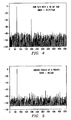
- Figure 4 shows the output spectrum of a 10-bit ADC with a nonlinear sample-and-hold circuit.
- the signal-to-noise ratio is about 37 dB for sinusoidal input.
- Figure 5 shows the output spectrum of a 10-bit ADC when the reference to the comparator array is pinned at four points, namely with four replica sample-and-holds.
- the signal-to-noise ratio improves to approximately 58 dB.
- the signal-to-noise ratio is 61.5 dB, very close to the ideal signal-to-noise ratio of a 10-bit converter of 62.03 dB with a linear sample-and-hold circuit.
Landscapes
- Physics & Mathematics (AREA)
- Nonlinear Science (AREA)
- Engineering & Computer Science (AREA)
- Theoretical Computer Science (AREA)
- General Physics & Mathematics (AREA)
- Optics & Photonics (AREA)
- Analogue/Digital Conversion (AREA)
Abstract
Description
Claims (6)
- An analog-to-digital converter for converting an analog signal to a digital signal, comprising:a sample-and-hold circuit for sampling said analog signal, holding said analog signal, and for outputting a held analog signal;a reference circuit for generating a reference voltage to be used as a threshold voltage;a comparator circuit for comparing said threshold voltage with said held analog signal; anda replica sample-and-hold circuit coupled between said comparator circuit and said reference circuit.
- An analog-to-digital converter as recited in Claim 1, wherein said replica sample-and-hold circuit is adapted to lower the threshold voltage of said comparator circuit.
- An analog-to-digital converter as recited in Claim 1 or Claim 2, wherein said replica sample-and-hold circuit has substantially the same nonlinearity as said sample-and-hold circuit.
- An analog-to-digital converter as recited in any of Claims 1-3, wherein said replica sample-and-hold circuit has the similar characteristics to said sample-and-hold circuit.
- An analog-to-digital converter as recited in any of Claims 1-4, wherein said replica sample-and-hold circuit has substantially the same current characteristics as said sample-and-hold circuit.
- An analog-to-digital converter as recited in any of Claims 1-5, wherein said replica sample-and-hold circuit has substantially the same voltage characteristics as said sample-and-hold circuit.
Applications Claiming Priority (2)
| Application Number | Priority Date | Filing Date | Title |
|---|---|---|---|
| US71370600A | 2000-11-15 | 2000-11-15 | |
| US713706 | 2000-11-15 |
Publications (3)
| Publication Number | Publication Date |
|---|---|
| EP1207624A2 true EP1207624A2 (en) | 2002-05-22 |
| EP1207624A3 EP1207624A3 (en) | 2004-07-14 |
| EP1207624B1 EP1207624B1 (en) | 2007-03-14 |
Family
ID=24867192
Family Applications (1)
| Application Number | Title | Priority Date | Filing Date |
|---|---|---|---|
| EP01000632A Expired - Lifetime EP1207624B1 (en) | 2000-11-15 | 2001-11-15 | Distortion compensation technique for flash-type analog-to-digital converters |
Country Status (6)
| Country | Link |
|---|---|
| EP (1) | EP1207624B1 (en) |
| JP (1) | JP2002330070A (en) |
| KR (1) | KR20020037720A (en) |
| AT (1) | ATE357082T1 (en) |
| DE (1) | DE60127223T2 (en) |
| TW (1) | TW513862B (en) |
Cited By (2)
| Publication number | Priority date | Publication date | Assignee | Title |
|---|---|---|---|---|
| US7646323B2 (en) | 2007-02-09 | 2010-01-12 | Texas Instruments Incorporated | Clock generator |
| CN101917195A (en) * | 2010-08-18 | 2010-12-15 | 中国电子科技集团公司第五十八研究所 | A High Precision Low Offset Charge Comparator Circuit |
Families Citing this family (1)
| Publication number | Priority date | Publication date | Assignee | Title |
|---|---|---|---|---|
| US11363231B2 (en) | 2020-09-07 | 2022-06-14 | Samsung Electronics Co., Ltd. | Image sensor |
Family Cites Families (2)
| Publication number | Priority date | Publication date | Assignee | Title |
|---|---|---|---|---|
| JPS5441061A (en) * | 1977-09-08 | 1979-03-31 | Sony Corp | Analogue/digital converter |
| JP2945805B2 (en) * | 1992-10-01 | 1999-09-06 | 松下電器産業株式会社 | A / D converter |
-
2001
- 2001-11-15 JP JP2001388489A patent/JP2002330070A/en active Pending
- 2001-11-15 KR KR1020010071028A patent/KR20020037720A/en not_active Withdrawn
- 2001-11-15 DE DE60127223T patent/DE60127223T2/en not_active Expired - Lifetime
- 2001-11-15 EP EP01000632A patent/EP1207624B1/en not_active Expired - Lifetime
- 2001-11-15 TW TW090128357A patent/TW513862B/en not_active IP Right Cessation
- 2001-11-15 AT AT01000632T patent/ATE357082T1/en not_active IP Right Cessation
Cited By (2)
| Publication number | Priority date | Publication date | Assignee | Title |
|---|---|---|---|---|
| US7646323B2 (en) | 2007-02-09 | 2010-01-12 | Texas Instruments Incorporated | Clock generator |
| CN101917195A (en) * | 2010-08-18 | 2010-12-15 | 中国电子科技集团公司第五十八研究所 | A High Precision Low Offset Charge Comparator Circuit |
Also Published As
| Publication number | Publication date |
|---|---|
| EP1207624B1 (en) | 2007-03-14 |
| ATE357082T1 (en) | 2007-04-15 |
| DE60127223D1 (en) | 2007-04-26 |
| TW513862B (en) | 2002-12-11 |
| DE60127223T2 (en) | 2008-01-10 |
| JP2002330070A (en) | 2002-11-15 |
| KR20020037720A (en) | 2002-05-22 |
| EP1207624A3 (en) | 2004-07-14 |
Similar Documents
| Publication | Publication Date | Title |
|---|---|---|
| US6617992B2 (en) | Capacitor mismatch independent gain stage for differential pipeline analog to digital converters | |
| US6784824B1 (en) | Analog-to-digital converter which is substantially independent of capacitor mismatch | |
| US11424754B1 (en) | Noise-shaping analog-to-digital converter | |
| US7852253B2 (en) | Digitally adjustable quantization circuit | |
| US9344106B2 (en) | ADC calibration | |
| US5936566A (en) | Auto-reference pseudo-flash analog to digital converter | |
| US7486218B2 (en) | Cyclic analog-to-digital converter | |
| EP0760181B1 (en) | Reference ladder auto-calibration circuit for an analog to digital converter | |
| KR101603892B1 (en) | Successive approxiamtion analog digital converter and converting method | |
| US6600440B1 (en) | Capacitor mismatch independent gain stage for pipeline analog to digital converters | |
| CN110995268B (en) | Multi-order successive approximation n-bit analog-to-digital converter | |
| JPH01265619A (en) | Analog/digital converter with compensated integral linear error and its operation | |
| US20030098808A1 (en) | Differential input A/D converter | |
| US8274419B2 (en) | Analog-digital converter with pipeline architecture associated with a programmable gain amplifier | |
| US7209060B2 (en) | Reducing variation in reference voltage when the load varies dynamically | |
| US7095356B1 (en) | Providing reference voltage with desired accuracy in a short duration to a dynamically varying load | |
| EP1207624B1 (en) | Distortion compensation technique for flash-type analog-to-digital converters | |
| CN114124099B (en) | Input scaling module of incremental analog-to-digital converter | |
| KR101902119B1 (en) | Successive approximation ad converter using switched-capacitor da convertor | |
| Bindra et al. | Range pre-selection sampling technique to reduce input drive energy for SAR ADCs | |
| US10693484B1 (en) | Pipelined analog-to-digital converter calibration | |
| US6798370B1 (en) | Parallel A/D converter | |
| US7348916B2 (en) | Pipeline A/D converter and method of pipeline A/D conversion | |
| KR102398446B1 (en) | Analog-digital converter | |
| Shu et al. | A 10$\sim $15-bit 60-MS/s Floating-Point ADC With Digital Gain and Offset Calibration |
Legal Events
| Date | Code | Title | Description |
|---|---|---|---|
| PUAI | Public reference made under article 153(3) epc to a published international application that has entered the european phase |
Free format text: ORIGINAL CODE: 0009012 |
|
| AX | Request for extension of the european patent |
Free format text: AL;LT;LV;MK;RO;SI |
|
| PUAL | Search report despatched |
Free format text: ORIGINAL CODE: 0009013 |
|
| AK | Designated contracting states |
Kind code of ref document: A3 Designated state(s): AT BE CH CY DE DK ES FI FR GB GR IE IT LI LU MC NL PT SE TR |
|
| AX | Request for extension of the european patent |
Extension state: AL LT LV MK RO SI |
|
| 17P | Request for examination filed |
Effective date: 20050114 |
|
| AKX | Designation fees paid |
Designated state(s): AT BE CH CY DE DK ES FI FR GB GR IE IT LI LU MC NL PT SE TR |
|
| GRAP | Despatch of communication of intention to grant a patent |
Free format text: ORIGINAL CODE: EPIDOSNIGR1 |
|
| RIN1 | Information on inventor provided before grant (corrected) |
Inventor name: PAVAN, SHANTHI Y. |
|
| GRAS | Grant fee paid |
Free format text: ORIGINAL CODE: EPIDOSNIGR3 |
|
| GRAA | (expected) grant |
Free format text: ORIGINAL CODE: 0009210 |
|
| AK | Designated contracting states |
Kind code of ref document: B1 Designated state(s): AT BE CH CY DE DK ES FI FR GB GR IE IT LI LU MC NL PT SE TR |
|
| PG25 | Lapsed in a contracting state [announced via postgrant information from national office to epo] |
Ref country code: FI Free format text: LAPSE BECAUSE OF FAILURE TO SUBMIT A TRANSLATION OF THE DESCRIPTION OR TO PAY THE FEE WITHIN THE PRESCRIBED TIME-LIMIT Effective date: 20070314 Ref country code: BE Free format text: LAPSE BECAUSE OF FAILURE TO SUBMIT A TRANSLATION OF THE DESCRIPTION OR TO PAY THE FEE WITHIN THE PRESCRIBED TIME-LIMIT Effective date: 20070314 Ref country code: NL Free format text: LAPSE BECAUSE OF FAILURE TO SUBMIT A TRANSLATION OF THE DESCRIPTION OR TO PAY THE FEE WITHIN THE PRESCRIBED TIME-LIMIT Effective date: 20070314 Ref country code: AT Free format text: LAPSE BECAUSE OF FAILURE TO SUBMIT A TRANSLATION OF THE DESCRIPTION OR TO PAY THE FEE WITHIN THE PRESCRIBED TIME-LIMIT Effective date: 20070314 Ref country code: CH Free format text: LAPSE BECAUSE OF FAILURE TO SUBMIT A TRANSLATION OF THE DESCRIPTION OR TO PAY THE FEE WITHIN THE PRESCRIBED TIME-LIMIT Effective date: 20070314 Ref country code: LI Free format text: LAPSE BECAUSE OF FAILURE TO SUBMIT A TRANSLATION OF THE DESCRIPTION OR TO PAY THE FEE WITHIN THE PRESCRIBED TIME-LIMIT Effective date: 20070314 |
|
| REG | Reference to a national code |
Ref country code: GB Ref legal event code: FG4D |
|
| REG | Reference to a national code |
Ref country code: CH Ref legal event code: EP |
|
| REF | Corresponds to: |
Ref document number: 60127223 Country of ref document: DE Date of ref document: 20070426 Kind code of ref document: P |
|
| REG | Reference to a national code |
Ref country code: IE Ref legal event code: FG4D |
|
| PG25 | Lapsed in a contracting state [announced via postgrant information from national office to epo] |
Ref country code: SE Free format text: LAPSE BECAUSE OF FAILURE TO SUBMIT A TRANSLATION OF THE DESCRIPTION OR TO PAY THE FEE WITHIN THE PRESCRIBED TIME-LIMIT Effective date: 20070614 |
|
| PG25 | Lapsed in a contracting state [announced via postgrant information from national office to epo] |
Ref country code: ES Free format text: LAPSE BECAUSE OF FAILURE TO SUBMIT A TRANSLATION OF THE DESCRIPTION OR TO PAY THE FEE WITHIN THE PRESCRIBED TIME-LIMIT Effective date: 20070625 |
|
| ET | Fr: translation filed | ||
| PG25 | Lapsed in a contracting state [announced via postgrant information from national office to epo] |
Ref country code: PT Free format text: LAPSE BECAUSE OF FAILURE TO SUBMIT A TRANSLATION OF THE DESCRIPTION OR TO PAY THE FEE WITHIN THE PRESCRIBED TIME-LIMIT Effective date: 20070814 |
|
| NLV1 | Nl: lapsed or annulled due to failure to fulfill the requirements of art. 29p and 29m of the patents act | ||
| REG | Reference to a national code |
Ref country code: CH Ref legal event code: PL |
|
| PLBE | No opposition filed within time limit |
Free format text: ORIGINAL CODE: 0009261 |
|
| STAA | Information on the status of an ep patent application or granted ep patent |
Free format text: STATUS: NO OPPOSITION FILED WITHIN TIME LIMIT |
|
| PG25 | Lapsed in a contracting state [announced via postgrant information from national office to epo] |
Ref country code: DK Free format text: LAPSE BECAUSE OF FAILURE TO SUBMIT A TRANSLATION OF THE DESCRIPTION OR TO PAY THE FEE WITHIN THE PRESCRIBED TIME-LIMIT Effective date: 20070314 |
|
| 26N | No opposition filed |
Effective date: 20071217 |
|
| PG25 | Lapsed in a contracting state [announced via postgrant information from national office to epo] |
Ref country code: IT Free format text: LAPSE BECAUSE OF FAILURE TO SUBMIT A TRANSLATION OF THE DESCRIPTION OR TO PAY THE FEE WITHIN THE PRESCRIBED TIME-LIMIT Effective date: 20070314 Ref country code: GR Free format text: LAPSE BECAUSE OF FAILURE TO SUBMIT A TRANSLATION OF THE DESCRIPTION OR TO PAY THE FEE WITHIN THE PRESCRIBED TIME-LIMIT Effective date: 20070615 |
|
| PG25 | Lapsed in a contracting state [announced via postgrant information from national office to epo] |
Ref country code: MC Free format text: LAPSE BECAUSE OF NON-PAYMENT OF DUE FEES Effective date: 20071130 |
|
| PG25 | Lapsed in a contracting state [announced via postgrant information from national office to epo] |
Ref country code: IE Free format text: LAPSE BECAUSE OF NON-PAYMENT OF DUE FEES Effective date: 20071115 |
|
| PG25 | Lapsed in a contracting state [announced via postgrant information from national office to epo] |
Ref country code: CY Free format text: LAPSE BECAUSE OF FAILURE TO SUBMIT A TRANSLATION OF THE DESCRIPTION OR TO PAY THE FEE WITHIN THE PRESCRIBED TIME-LIMIT Effective date: 20070314 |
|
| PG25 | Lapsed in a contracting state [announced via postgrant information from national office to epo] |
Ref country code: LU Free format text: LAPSE BECAUSE OF NON-PAYMENT OF DUE FEES Effective date: 20071115 |
|
| PG25 | Lapsed in a contracting state [announced via postgrant information from national office to epo] |
Ref country code: TR Free format text: LAPSE BECAUSE OF FAILURE TO SUBMIT A TRANSLATION OF THE DESCRIPTION OR TO PAY THE FEE WITHIN THE PRESCRIBED TIME-LIMIT Effective date: 20070314 |
|
| REG | Reference to a national code |
Ref country code: FR Ref legal event code: PLFP Year of fee payment: 15 |
|
| REG | Reference to a national code |
Ref country code: FR Ref legal event code: PLFP Year of fee payment: 16 |
|
| PGFP | Annual fee paid to national office [announced via postgrant information from national office to epo] |
Ref country code: GB Payment date: 20161026 Year of fee payment: 16 Ref country code: FR Payment date: 20161017 Year of fee payment: 16 Ref country code: DE Payment date: 20161130 Year of fee payment: 16 |
|
| REG | Reference to a national code |
Ref country code: DE Ref legal event code: R119 Ref document number: 60127223 Country of ref document: DE |
|
| GBPC | Gb: european patent ceased through non-payment of renewal fee |
Effective date: 20171115 |
|
| REG | Reference to a national code |
Ref country code: FR Ref legal event code: ST Effective date: 20180731 |
|
| PG25 | Lapsed in a contracting state [announced via postgrant information from national office to epo] |
Ref country code: DE Free format text: LAPSE BECAUSE OF NON-PAYMENT OF DUE FEES Effective date: 20180602 Ref country code: FR Free format text: LAPSE BECAUSE OF NON-PAYMENT OF DUE FEES Effective date: 20171130 |
|
| PG25 | Lapsed in a contracting state [announced via postgrant information from national office to epo] |
Ref country code: GB Free format text: LAPSE BECAUSE OF NON-PAYMENT OF DUE FEES Effective date: 20171115 |