EP1205999A2 - High frequency filter, filter device, and electronic apparatus incorporating the same - Google Patents
High frequency filter, filter device, and electronic apparatus incorporating the same Download PDFInfo
- Publication number
- EP1205999A2 EP1205999A2 EP01127032A EP01127032A EP1205999A2 EP 1205999 A2 EP1205999 A2 EP 1205999A2 EP 01127032 A EP01127032 A EP 01127032A EP 01127032 A EP01127032 A EP 01127032A EP 1205999 A2 EP1205999 A2 EP 1205999A2
- Authority
- EP
- European Patent Office
- Prior art keywords
- high frequency
- frequency filter
- microstrip line
- filter
- hole
- Prior art date
- Legal status (The legal status is an assumption and is not a legal conclusion. Google has not performed a legal analysis and makes no representation as to the accuracy of the status listed.)
- Withdrawn
Links
Images



Classifications
-
- H—ELECTRICITY
- H01—ELECTRIC ELEMENTS
- H01P—WAVEGUIDES; RESONATORS, LINES, OR OTHER DEVICES OF THE WAVEGUIDE TYPE
- H01P1/00—Auxiliary devices
- H01P1/20—Frequency-selective devices, e.g. filters
- H01P1/201—Filters for transverse electromagnetic waves
- H01P1/203—Strip line filters
-
- H—ELECTRICITY
- H01—ELECTRIC ELEMENTS
- H01P—WAVEGUIDES; RESONATORS, LINES, OR OTHER DEVICES OF THE WAVEGUIDE TYPE
- H01P1/00—Auxiliary devices
- H01P1/20—Frequency-selective devices, e.g. filters
- H01P1/201—Filters for transverse electromagnetic waves
- H01P1/203—Strip line filters
- H01P1/2039—Galvanic coupling between Input/Output
Definitions
- the present invention relates to high frequency filters and filter devices using the filters.
- the invention also relates to electronic apparatuses incorporating the same.
- a ground electrode is arranged on one of the main surfaces of a dielectric substrate and microstrip lines are formed on the other main surface of the substrate to form a plurality of resonators.
- a through-hole is often used to connect the microstrip lines to the ground electrode.
- Japanese Unexamined Patent Application Publication No. 7-86802 describes a high frequency filter using through-holes as resonators.
- This high frequency filter includes resonators formed by using the inductance and the capacitance of the through-holes.
- the plurality of resonators are electrically coupled to each other via a capacitance at the gap between electrodes formed on one of the main surfaces of a dielectric substrate to constitute the high frequency filter.
- the high frequency filter using the through-holes as resonators has a problem in that it is difficult to adjust the characteristics of the resonators.
- the diameters of the through-holes need to be changed.
- the dielectric substrate must be replaced, which takes time and increases cost.
- accurate adjustments are unlikely to be expected.
- the inter-electrode gap which serves as an additional capacitance element, is used to couple the resonators, the size of the filter increases.
- the present invention is able to provide a high frequency filter which facilitates filter-characteristic adjustments and achieves miniaturization. Furthermore, by increasing the inter-resonator coupling coefficient, a broadband characteristic is obtainable.
- the invention is further able to provide a filter device using the high frequency filter and an electronic apparatus incorporating the same.
- a high frequency filter including a dielectric substrate, a ground electrode arranged on a main surface of the dielectric substrate, a through-hole, and a plurality of microstrip line resonators formed on the other main surface of the dielectric substrate, a first end of each resonator being grounded via the through-hole.
- the microstrip line resonators share the through-hole for grounding the first end of each resonator, and the resonators are mutually coupled via the inductance of the through-hole.
- a high frequency filter including a dielectric substrate, a ground electrode arranged on a main surface of the dielectric substrate, a through-hole, and two microstrip line resonators formed on the other main surface of the dielectric substrate, a first end of each resonator being grounded via the through-hole.
- the two microstrip line resonators share the through-hole for grounding the first end of each resonator, and the resonators are mutually coupled via the inductance of the through-hole.
- the two microstrip line resonators may be spirally formed by being wound in mutually opposite directions.
- a side edge of one of the two microstrip line resonators may be arranged near a side edge of the other microstrip line resonator to mutually couple the resonators inductively.
- a second end of one of the two microstrip line resonators may be opposed to the side edge of the other microstrip line resonator to mutually couple the resonators capacitively.
- the high frequency filter according to one of the first and second aspects may further include input/output electrodes or wires, each being connected to a point disposed between the first end and the second end of a respective microstrip line resonator.
- a filter device including the high frequency filter according to one of the first and second aspects of the invention.
- an electronic apparatus including the high frequency filter according to one of the first and second aspects or the above filter device.
- the filter characteristics can be easily adjusted and miniaturization can be achieved. Moreover, by making the coupling coefficient for coupling between the resonators larger, a broadband characteristic can be obtained.
- Fig. 1 shows a perspective view of a high frequency filter according to an embodiment of the present invention.
- a high frequency filter I includes a dielectric substrate 2, a ground electrode 3 arranged substantially on an entire main surface of the dielectric substrate 2, two microstrip lines 4a and 5a arranged on the other main surface of the dielectric substrate 2, a through-hole 6 formed at the junction of the two microstrip lines 4a and 5a, and signal output/input wires 7 and 8 connected to the two microstrip lines 4a and 5a.
- Each of the wires 7 and 8 is also connected to an outside circuit, which is not shown here.
- the microstrip line 4a and the through-hole 6 constitute a 1/4-wavelength microstrip line resonator 4 with one end grounded and the other end open-circuited.
- the microstrip line 5a and the through-hole 6 constitute a 1/4-wavelength microstrip line resonator 5 with one end grounded and the other end open-circuited.
- the microstrip line resonators 4 and 5 share the through-hole 6.
- Fig. 2 shows an equivalent circuit diagram of the high frequency filter 1.
- the two microstrip lines 4a and 5a are connected to each other, and the junction of the lines 4a and 5a is grounded via a series circuit composed of an inductor Lt and a resistor Rt as equivalent-circuit elements of the through-hole 6.
- the microstrip line resonator 4 formed by the microstrip line 4a and the through-hole 6 is coupled to the microstrip line resonator 5 formed by the microstrip line 5a and the through-hole 6 via the inductor Lt as the inductance of the through-hole 6.
- a port 1 represents the wire 7
- a port 2 represents the wire 8.
- This circuit generates an odd-mode resonant frequency (fodd) determined by the lengths of the microstrip lines 4a and 5a and an even-mode resonant frequency (feven) including the inductor Lt of the through-hole 6.
- odd-mode resonant frequency (fodd) determined by the lengths of the microstrip lines 4a and 5a
- even-mode resonant frequency (feven) including the inductor Lt of the through-hole 6.
- the wires 7 and 8 are used to couple the high frequency filter 1 to outside circuits.
- the external Q (Qe) of the high frequency filter 1 can be varied by changing the positions where the wires 7 and 8 are connected to the two microstrip lines 4a and 5a.
- the external Q can be adjusted by adjusting the positions for connecting the wires.
- the two microstrip line resonators 4 and 5 are magnetically coupled to each other via the inductance Lt of the through-hole 6.
- the high frequency filter 1 can be made compact.
- a larger coupling coefficient can be obtained in the case of magnetic coupling obtained by the inductance Lt of the through-hole 6, as compared with the case of electrical coupling obtained by a capacitive element such as the gap between electrodes in conventional filters.
- a larger coupling coefficient can be obtained.
- the high frequency filter 1 can easily be given a broadband characteristic.
- Fig. 3 shows a plan view of a high frequency filter according to another embodiment of the invention.
- the reference numerals used in the high frequency filter shown in Fig. 1 are given to the same and equivalent parts of the filter shown in Fig. 3, and the explanation of the parts will not be given.
- taps 11 and 12 made of narrower microstrip lines to connect to outside circuits.
- FIG. 4 shows a plan view of a high frequency filter according to another embodiment of the invention.
- the reference numerals used in the high frequency filter 1 shown in Fig. 1 are given to the same and equivalent parts in the filter shown in Fig. 4, and no explanation of the parts will be provided.
- the high frequency filter 15 and the outside circuits are coupled via capacitances C1 and C2 generated between the input/output electrodes 16, 17, and the microstrip lines 4a and 5a. Adjustments can be made to external Q by adjusting the capacitances C1 and C2.
- this embodiment can also provide substantially the same advantages as those obtained in the high frequency filter 1 using the wires 7 and 8.
- Fig. 5 shows a plan view of a high frequency filter according to another embodiment of the invention.
- the reference numerals used in Fig. 1 are given to the same and equivalent parts of the filter and the explanation of the parts will be omitted.
- a high frequency filter 20 including two microstrip lines 21a and 22a arranged on a main surface of a dielectric substrate 2, a through-hole 6 formed at the junction of the microstrip lines 21a and 22a, and signal input/output wires 7 and 8 connected to the microstrip lines 21a and 22a.
- the microstrip line 21a and the through-hole 6 constitute a 1/4-wavelength microstrip line resonator 21 with a first end grounded and the second end open-circuited.
- the microstrip line 22a and the through-hole 6 constitute a 1/4-wavelength microstrip line resonator 22 with a first end grounded and the second end open-circuited.
- the microstrip line resonators 21 and 22 share the through-hole 6.
- the microstrip lines 21a and 22a are spirally formed by being wound in mutually opposite directions to make an overall S-shaped configuration.
- the second end of the microstrip line 21a is arranged near a side edge near the first end of the microstrip line 22a.
- the second end of the microstrip line 22a is arranged near a side edge near the first end of the microstrip line 21a.
- the high frequency filter 20 can be miniaturized.
- magnetic couplings M are generated at the parts where side edges on the open-circuited end sides of the microstrip lines 21a and 22a are arranged near the side edges on the grounded-end sides of the microstrip lines 22a and 21a, respectively.
- the microstrip line resonators 21 and 22 are coupled not only via the inductance of the through-hole 6 but also by the magnetic couplings M between the microstrip lines 21a and 22a.
- the magnetic couplings M can compensate for an insufficiency of the coupling provided by the inductance of the through-hole 6.
- the magnetic couplings M between the microstrip lines 21a and 22a can compensate for the insufficiency of the coupling provided by the through-hole. Furthermore, by adjusting the gaps between the mutually adjacent parts of the strip lines 21a and 22a, the magnitudes of the magnetic couplings M can be controlled, thereby increasing the freedom of design of the high frequency filter 20.
- Fig. 6 shows a plan view of a high frequency filter according to another embodiment of the invention.
- the reference numerals used in Fig. 1 are given to the same and equivalent parts and the explanation of the parts will be omitted.
- each of microstrip lines 26a and 27a of a high frequency filter 25 has a length such that it forms a spiral shape of approximately 1.5 turn.
- the microstrip line 26a and a through-hole 6 constitute a 1/4-wavelength microstrip line resonator 26 with one end grounded and the other end open-circuited.
- the microstrip line 27a and the through-hole 6 constitute a 1/4-wavelength microstrip line resonator 27 with one end grounded and the other end open-circuited.
- the microstrip line resonators 26 and 27 share the through-hole 6.
- a part of the microstrip line 26a is adjacent to a side edge near the first end of the microstrip line 27a.
- a part of the microstrip line 27a is adjacent to a side edge near the first end of the microstrip line 26a.
- the high frequency filter 25 having the above structure, also, since magnetic couplings M are generated between the microstrip lines 26a and 27a, the same advantages as those obtained in the high frequency filter 20 can be obtained. Additionally, since the lengths of the microstrip lines 26a and 27a can be increased, the high frequency filter 25 can be made smaller than the high frequency filter 20.
- the high frequency filter 25 adopts a step-impedance configuration, in which the closer to the second ends (the open-circuited ends) of the microstrip lines 26a and 27a, the narrower the line widths.
- a 1/4-wavelength resonator resonance is produced even at a frequency three times as high as a fundamental resonant frequency.
- inductances at the second ends of the microstrip line resonators increase.
- the frequency of the resonator becomes lower than three times as high as the resonant frequency.
- the high frequency filter 25 has an advantage in which attenuation characteristics obtained at the frequency three times as high as the resonant frequency can be improved.
- Fig. 7 shows a plan view of a high frequency filter according to another embodiment of the invention.
- the reference numerals used in Fig. 5 are given to the same and equivalent parts and the explanation of the parts will be omitted.
- a high frequency filter 30 includes microstrip lines 31a and 32a formed on one of the main surfaces of a dielectric substrate 2, a through-hole 6 formed at the junction of the microstrip lines 31a and 32a, and signal input/output wires 7 and 8 connected to the microstrip lines 31a and 32a.
- the microstrip line 31a and the through-hole 6 constitute a 1/4-wavelength microstrip line resonator 31 with a first end grounded and the second end open-circuited.
- the microstrip line 32a and the through-hole 6 constitute a 1/4-wavelength microstrip line resonator 32 with a first end grounded and the second end open-circuited.
- the microstrip line resonators 31 and 32 share the through-hole 6.
- the microstrip lines 31a and 32a are spirally formed by being wound in mutually opposite directions to make an overall S-shaped configuration.
- the second end of the microstrip line 31a is arranged near a side edge near the first end of the microstrip line 32a.
- the second end of the microstrip line 32a is also arranged near a side edge near the first end of the microstrip line 31a.
- the second end of the microstrip line 31a is arranged near the side edge of the microstrip line 32a in a mutually opposing manner.
- the second end of the microstrip line 32a is arranged near the side edge of the microstrip line 31 a in a mutually opposing manner.
- the couplings can be adjusted without increasing the gaps between the microstrip lines 31a and 32a, by narrowing the gaps between the parts where the open-circuited ends of the microstrip lines 31a and 32a are opposed to the side edges of the microstrip lines 32a and 31a to increase the coupling capacitances C3 and C4.
- the high frequency filter 30 can be made smaller than the high frequency filter 20.
- Fig. 8 shows experimental results regarding a correlation between the gap g between the part where the open-circuited end of one of the microstrip lines is opposed to the side edge of the other microstrip line, and the coupling coefficient k which defines the coupling between the microstrip line resonators 31 and 32 in the high frequency filter 30.
- the coupling coefficient k becomes smaller.
- the coupling coefficient k obtained only via the inductance Lt of the through-hole 6 is 0.122.
- the coupling coefficient k becomes larger than 0.122.
- the relative permittivity of a dielectric substrate used in this experiment is 110.
- the substrate is 0.3 mm thick and the diameter of the through-hole is 145 mm long.
- the gaps between the parts where the two microstrip lines are arranged near each other are set to be 150 mm.
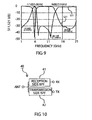
- Fig. 9 illustrates frequency characteristics S11 (reflection loss) and S21 (insertion loss) obtained when the high frequency filter 30 is actually produced as a band pass filter.
- the central frequency of the pass band is 5.8 GHz
- a 3-dB bandwidth of the pass band is 980 MHz
- insertion loss of the pass-band is -1.1 dB at 5.8 GHz.
- characteristics such as -22.4 dB at 2.9 GHz as an attenuation band, -44.1 GHz at 11.6 GHz, and -30.9 dB at 17.4 GHz.
- the frequency 17.4 GHz is equivalent to a frequency approximately three times as high as the central frequency 5.8 GHz.
- the high frequency filter 30 adopts the step-impedance structure in which the open-circuited ends of the microstrip line resonators 31 and 32 have narrower widths. With this arrangement, the frequency, which should primarily be three times as high as the fundamental resonant frequency, is shifted to near the frequency of approximately 13.5 GHz lower than that. As a result, attenuation characteristic obtained at 17.4 GHz is -30.9 dB, which is an excellent value.
- Fig. 10 shows a block diagram of a duplexer, which is an example of a filter device according to an embodiment of the invention.
- a duplexer 40 shown in Fig. 10 one end of a reception filter BPF 41 and one end of a transmission filter BPF 42, in which the filters have mutually different pass bands, are connected to each other to form an antenna terminal ANT.
- the other end of the reception filter BPF 41 is arranged as a reception terminal RX and the other end of transmission filter BPF 42 is arranged as a transmission terminal TX.
- the reception filter BPF 41 and the transmission filter BPF 42 for example, the high frequency filters shown in Fig. 1 and Figs. 3 to 7 are used. Since the basic function and performance of the duplexer 40 is publicly known, the explanation of thereof will be omitted.
- the duplexer 40 having the above structure incorporates the high frequency filter of the invention, which can achieve miniaturization and can improve attenuation characteristics. Thus, significantly, miniaturization can be achieved and high performance capabilities can be obtained.
- the filter device of the invention is not limited to a duplexer and it includes all kinds of filter devices formed by using a single high frequency filter or a plurality of high frequency filters according to the invention. Even in this case, the same advantages as those obtained in the duplexer 40 can be obtained.
- Fig. 11 shows a block diagram of a communication apparatus which is an example of an electronic apparatus according to an embodiment of the invention.
- a communication apparatus 50 includes an antenna 51, the duplexer 40 of the invention shown in Fig. 10, a reception circuit 52, a transmission circuit 53, and a signal processing circuit 54.
- the antenna 51 is connected to an antenna terminal ANT of the duplexer 40.
- a reception terminal RX included in the duplexer 40 is connected to the signal processing circuit 54 via the reception circuit 52.
- the signal processing circuit 54 is connected to a transmission terminal TX included in the duplexer 40 via the transmission circuit 53.
- the basic function and performance of the communication apparatus 50 is publicly known. Thus, the explanation thereof will be omitted here.
- the communication apparatus 50 incorporates the duplexer 40 as the filter device of the invention, miniaturization can be achieved and high performance capabilities can be obtained.
- the electronic apparatus of the invention is limited neither to a communication apparatus nor to an apparatus including the filter device of the invention.
- the electronic apparatus of the invention includes all kinds of electronic apparatuses. For example, only the high frequency filter of the invention may be used or both of the high frequency filter and the filter device of the invention may be used. In either case, the same advantages as those obtained in the communication apparatus 50 can be obtained.
- a plurality of microstrip line resonators in which one end of each line is grounded via a through-hole, shares the through-hole to be mutually coupled via the inductance of the through-hole.
- the coupling coefficient for coupling between the microstrip line resonators can be made larger, the high frequency filter can obtain a broadband characteristic.
- the side edge of one of the two microstrip line resonators may be arranged close to the side edge of the other microstrip line resonator to be magnetically coupled.
- the coupling coefficient is made larger so that the high frequency filter can obtain a broader band characteristic.
- the other end of one of the two microstrip line resonators may be opposed to the side edge of the other microstrip line resonator to be electrically coupled to each other via a capacitance.
- the input/output wire or electrode is connected at a point located between one end and the other end of each microstrip line resonator, to be connected to an outside circuit.
- the filter device of the invention by using the high frequency filter according to the invention, miniaturization can be achieved and high performance capabilities can be obtained.
- the electronic apparatus of the invention by using the high frequency filter or the filter device according to the invention, miniaturization can be achieved and high performance capabilities can be obtained.
Landscapes
- Physics & Mathematics (AREA)
- Electromagnetism (AREA)
- Control Of Motors That Do Not Use Commutators (AREA)
- Waveguides (AREA)
Abstract
Description
In addition, the second end of the microstrip line 31a is arranged near the side edge of the microstrip line 32a in a mutually opposing manner. The second end of the microstrip line 32a is arranged near the side edge of the microstrip line 31 a in a mutually opposing manner. With this arrangement, coupling capacitances C3 and C4 are generated at the opposing parts to provide electrical couplings. The electrical couplings perform a function of canceling the magnetic couplings M between the microstrip lines 31a and 32a.
Claims (10)
- A high frequency filter (1; 10; 15; 20; 25; 30) comprising:wherein the microstrip line resonators (4, 5; 21, 22; 26, 27; 31, 32) share the through-hole (6) for grounding the one end of each resonator (4, 5; 21, 22; 26, 27; 31, 32) to be mutually coupled via the inductance of the through-hole (6).a dielectric substrate (2);a ground electrode (3) arranged on a main surface of the dielectric substrate (2);a conductive through-hole (6); anda plurality of microstrip line resonators (4, 5; 21, 22; 26, 27; 31, 32) formed on the other main surface of the dielectric substrate (2), one end of each resonator (4, 5; 21, 22; 26, 27; 31, 32) being grounded via the through-hole (6);
- A high frequency filter (1; 10; 15; 20; 25; 30) comprising:wherein the two microstrip line resonators (4, 5; 21, 22; 26, 27; 31, 32) share the through-hole (6) for grounding the one end of each resonator (4, 5; 21, 22; 26, 27; 31, 32) to be mutually coupled via the inductance of the through-hole (6).a dielectric substrate (2);a ground electrode (3) arranged on a main surface of the dielectric substrate (2);a conductive through-hole (6); andtwo microstrip line resonators (4, 5; 21, 22; 26, 27; 31, 32) formed on the other main surface of the dielectric substrate (2), a first end of each resonator (4, 5; 21, 22; 26, 27; 31, 32) being grounded via the through-hole (6);
- The high frequency filter (25) according to Claim 2, wherein the two microstrip line resonators (26, 27) are spirally formed by being wound on said dielectric substrate (2) in mutually opposite directions.
- The high frequency filter (25) according to Claim 3, wherein the second end of one of the two microstrip line resonators (26, 27) is opposed to the side edge of the other microstrip line resonator (26, 27) so as to generate a capacitance to mutually couple the resonators (26, 27).
- The high frequency filter (20; 25; 30) according to Claim 2 or 3, wherein a side edge of one of the two microstrip line resonators (21, 22; 26, 27; 31, 32) is arranged near a side edge of the other microstrip line resonator (21, 22; 26, 27; 31, 32) to mutually couple the resonators (21, 22; 26, 27; 31, 32).
- The high frequency filter (30) according to Claim 2, 3 or 5, wherein the second end of one of the two microstrip line resonators (31,32) is opposed to the side edge of the other microstrip line resonator (31,32) so as to generate a capacitance to mutually couple the resonators (31, 32).
- The high frequency filter (1; 20; 25; 30) according to one of claims 1 to 6, further comprising input/output wires (7, 8; 11, 12) connected to respective ones of the microstrip line resonators (4, 5; 21, 22; 26, 27; 31, 32).
- A filter device (40) comprising the high frequency filter (1; 10; 15; 20; 25; 30) according to one of claims 1 to 7, and further comprising a pair of terminals (RX, TX) for connecting said filter into a circuit.
- An electronic apparatus (50) incorporating the filter device according to Claim 8, and further comprising a high-frequency circuit (52, 53) connected to at least one of said terminals (RX, TX).
- An electronic apparatus (50) incorporating the high frequency filter (1; 10; 15; 20; 25; 30) according to one of claims 1 to 7, and further comprising a high-frequency circuit (52, 53) connected to said filter (1; 10; 15; 20; 25; 30).
Applications Claiming Priority (2)
| Application Number | Priority Date | Filing Date | Title |
|---|---|---|---|
| JP2000346534 | 2000-11-14 | ||
| JP2000346534A JP3531603B2 (en) | 2000-11-14 | 2000-11-14 | High frequency filter, filter device using the same, and electronic device using the same |
Publications (2)
| Publication Number | Publication Date |
|---|---|
| EP1205999A2 true EP1205999A2 (en) | 2002-05-15 |
| EP1205999A3 EP1205999A3 (en) | 2003-07-16 |
Family
ID=18820387
Family Applications (1)
| Application Number | Title | Priority Date | Filing Date |
|---|---|---|---|
| EP01127032A Withdrawn EP1205999A3 (en) | 2000-11-14 | 2001-11-14 | High frequency filter, filter device, and electronic apparatus incorporating the same |
Country Status (4)
| Country | Link |
|---|---|
| US (1) | US6720849B2 (en) |
| EP (1) | EP1205999A3 (en) |
| JP (1) | JP3531603B2 (en) |
| KR (1) | KR100401967B1 (en) |
Cited By (1)
| Publication number | Priority date | Publication date | Assignee | Title |
|---|---|---|---|---|
| CN104332679A (en) * | 2013-07-22 | 2015-02-04 | 香港城市大学 | Microstrip line filter |
Families Citing this family (17)
| Publication number | Priority date | Publication date | Assignee | Title |
|---|---|---|---|---|
| JP4250718B2 (en) | 2004-04-30 | 2009-04-08 | 富士通コンポーネント株式会社 | Filter device and circuit module |
| US20050251769A1 (en) * | 2004-05-04 | 2005-11-10 | Frank Mark D | System and method for determining signal coupling in a circuit design |
| US7312676B2 (en) * | 2005-07-01 | 2007-12-25 | Tdk Corporation | Multilayer band pass filter |
| JP4327802B2 (en) * | 2006-01-23 | 2009-09-09 | 株式会社東芝 | Filter and wireless communication apparatus using the same |
| KR100710820B1 (en) * | 2006-04-13 | 2007-04-25 | 한국과학기술원 | Planar Helical Resonator and Ultra High Frequency Oscillator |
| JP4548383B2 (en) * | 2006-05-09 | 2010-09-22 | 株式会社村田製作所 | Non-reciprocal circuit device and communication device |
| KR100802358B1 (en) * | 2006-08-22 | 2008-02-13 | 주식회사 이엠따블유안테나 | Transmission line |
| KR100828948B1 (en) | 2006-10-30 | 2008-05-13 | 주식회사 이엠따블유안테나 | Interdigital Capacitors, Inductors, and Transmission Lines and Couplers Using Them |
| WO2008093626A1 (en) * | 2007-02-01 | 2008-08-07 | Murata Manufacturing Co., Ltd. | Chip element and process for producing the same |
| CN100492755C (en) * | 2007-05-19 | 2009-05-27 | 中国科学技术大学 | Broadband/ultra-broadband micro band filter using left and right mixing transmission line structure |
| JP4763741B2 (en) * | 2008-03-24 | 2011-08-31 | 双信電機株式会社 | Passive components |
| JP4972041B2 (en) * | 2008-06-25 | 2012-07-11 | パナソニック株式会社 | filter |
| JP5324497B2 (en) * | 2010-02-25 | 2013-10-23 | シャープ株式会社 | Filter and satellite broadcast receiving apparatus using the same |
| US8258897B2 (en) * | 2010-03-19 | 2012-09-04 | Raytheon Company | Ground structures in resonators for planar and folded distributed electromagnetic wave filters |
| DE102013017296A1 (en) * | 2013-10-18 | 2015-04-23 | IAD Gesellschaft für Informatik, Automatisierung und Datenverarbeitung mbH | Variable microstrip bandpass filter based on coupled λ / 4 resonators |
| JP6868046B2 (en) | 2019-02-08 | 2021-05-12 | 双信電機株式会社 | Resonator and filter |
| CN114650029B (en) * | 2022-03-02 | 2026-01-06 | 西安北方华创微电子装备有限公司 | A radio frequency (RF) filter circuit and a method for adjusting the RF filter circuit. |
Family Cites Families (7)
| Publication number | Priority date | Publication date | Assignee | Title |
|---|---|---|---|---|
| US4563773A (en) * | 1984-03-12 | 1986-01-07 | The United States Of America As Represented By The Secretary Of The Army | Monolithic planar doped barrier subharmonic mixer |
| SU1541691A1 (en) | 1988-02-15 | 1990-02-07 | Институт Физики Им.Л.В.Киренского | Method of manufacturing microstrip filter pattern |
| JPH0385903A (en) * | 1989-08-30 | 1991-04-11 | Kyocera Corp | Band pass filter |
| JPH05199010A (en) | 1992-01-21 | 1993-08-06 | Murata Mfg Co Ltd | Band pass filter |
| JPH0786802A (en) | 1993-09-14 | 1995-03-31 | Toshiba Corp | High frequency circuit |
| JP2908225B2 (en) | 1993-12-24 | 1999-06-21 | 日本電気株式会社 | High frequency choke circuit |
| JP3319377B2 (en) | 1998-01-30 | 2002-08-26 | 株式会社村田製作所 | Coplanar line filter and duplexer |
-
2000
- 2000-11-14 JP JP2000346534A patent/JP3531603B2/en not_active Expired - Lifetime
-
2001
- 2001-10-31 US US10/001,672 patent/US6720849B2/en not_active Expired - Lifetime
- 2001-11-12 KR KR10-2001-0070151A patent/KR100401967B1/en not_active Expired - Lifetime
- 2001-11-14 EP EP01127032A patent/EP1205999A3/en not_active Withdrawn
Cited By (1)
| Publication number | Priority date | Publication date | Assignee | Title |
|---|---|---|---|---|
| CN104332679A (en) * | 2013-07-22 | 2015-02-04 | 香港城市大学 | Microstrip line filter |
Also Published As
| Publication number | Publication date |
|---|---|
| US20020057143A1 (en) | 2002-05-16 |
| US6720849B2 (en) | 2004-04-13 |
| KR20020037688A (en) | 2002-05-22 |
| KR100401967B1 (en) | 2003-10-17 |
| JP3531603B2 (en) | 2004-05-31 |
| EP1205999A3 (en) | 2003-07-16 |
| JP2002151908A (en) | 2002-05-24 |
Similar Documents
| Publication | Publication Date | Title |
|---|---|---|
| US6720849B2 (en) | High frequency filter, filter device, and electronic apparatus incorporating the same | |
| CN100382384C (en) | Low Pass Filter and Cell Phone with Directional Coupler | |
| US6828881B2 (en) | Stacked dielectric filter | |
| US5424694A (en) | Miniature directional coupler | |
| KR0147726B1 (en) | Dielectric filter | |
| US5812036A (en) | Dielectric filter having intrinsic inter-resonator coupling | |
| JP2007013962A (en) | Multilayer bandpass filter | |
| CN110459839B (en) | A Frequency Tunable Differential Double Pass Band Filter | |
| CN100595972C (en) | Band-pass filter and wireless communication device using same | |
| EP0869572A2 (en) | Dielectric filter, dielectric duplexer, and communication apparatus using the same | |
| KR100577006B1 (en) | Microstrip Crosslink Bandpass Filter with Asymmetric Frequency Characteristics | |
| KR100249836B1 (en) | Duplexer with step-impedence resonator | |
| JP2001203503A (en) | Strip line filter, duplexer, filter, communication unit and characteristic adjustment method for the strip line filter | |
| JP3797273B2 (en) | Band stop filter and communication device | |
| US7495531B2 (en) | Filter and radio communication apparatus using the same | |
| KR100449226B1 (en) | Dielectric Duplexer | |
| KR100249838B1 (en) | High Frequency Filter with Citron Resonator | |
| US6809615B2 (en) | Band-pass filter and communication apparatus | |
| EP1184929A2 (en) | Dielectric filter, dielectric coupler, and communication device using the same | |
| CN1162937C (en) | Dielectric filter, dielectric duplexer and communication equipment system | |
| CN110364789A (en) | A kind of multifunctional reconfigurable filter based on short-circuit coupled line structure | |
| JP5519947B2 (en) | Band pass filter | |
| KR100330685B1 (en) | Monoblock dielectric filter with an attenuation pole | |
| CN116259940B (en) | A dual-passband filter composed of semi-lumped elements | |
| JP2001217609A (en) | Low-pass filter circuit and circuit board |
Legal Events
| Date | Code | Title | Description |
|---|---|---|---|
| PUAI | Public reference made under article 153(3) epc to a published international application that has entered the european phase |
Free format text: ORIGINAL CODE: 0009012 |
|
| 17P | Request for examination filed |
Effective date: 20011114 |
|
| AK | Designated contracting states |
Kind code of ref document: A2 Designated state(s): AT BE CH CY DE DK ES FI FR GB GR IE IT LI LU MC NL PT SE TR |
|
| AX | Request for extension of the european patent |
Free format text: AL;LT;LV;MK;RO;SI |
|
| PUAL | Search report despatched |
Free format text: ORIGINAL CODE: 0009013 |
|
| AK | Designated contracting states |
Designated state(s): AT BE CH CY DE DK ES FI FR GB GR IE IT LI LU MC NL PT SE TR |
|
| AX | Request for extension of the european patent |
Extension state: AL LT LV MK RO SI |
|
| AKX | Designation fees paid |
Designated state(s): DE FR GB |
|
| 17Q | First examination report despatched |
Effective date: 20070424 |
|
| R17C | First examination report despatched (corrected) |
Effective date: 20070717 |
|
| RAP1 | Party data changed (applicant data changed or rights of an application transferred) |
Owner name: MURATA MANUFACTURING CO., LTD. |
|
| STAA | Information on the status of an ep patent application or granted ep patent |
Free format text: STATUS: THE APPLICATION IS DEEMED TO BE WITHDRAWN |
|
| 18D | Application deemed to be withdrawn |
Effective date: 20121204 |