BACKGROUND OF THE INVENTION
Field of the Invention
This invention relates to an image information read-out
apparatus, and more particularly to an image information
read-out apparatus in which reading light is projected in a
line onto an image-bearing medium bearing thereon an image and
image-bearing light bearing thereon the image on the
image-bearing medium and emitted from the recording medium
upon exposure to the reading light is read out by a line sensor.
Description of the Related Art
When certain kinds of phosphor are exposed to a radiation,
they store a part of energy of the radiation. Then when the
phosphor which has been exposed to the radiation is exposed
to stimulating rays such as visible light or a laser beam, light
is emitted from the phosphor in proportion to the stored energy
of the radiation. A phosphor exhibiting such properties is
generally referred to as "a stimulable phosphor". In this
specification, the light emitted from the stimulable phosphor
upon stimulation thereof will be referred to as "stimulated
emission". There has been put into wide use as a computed
radiography a radiation image recording and reproducing system
using a stimulable phosphor sheet (a sheet provided with a layer
of the stimulable phosphor).
In the radiation image recording and reproducing system,
a stimulable phosphor sheet is exposed to a radiation passing
through an object such as a human body to have a radiation image
information of the object stored on the stimulable phosphor
sheet, a stimulating light beam such as a laser beam is caused
to two-dimensionally scan the stimulable phosphor sheet,
thereby causing each part of the stimulable phosphor sheet
exposed to the stimulating light beam to emit the stimulated
emission, the stimulated emission is photoelectrically
detected, thereby obtaining an image signal (a radiation image
signal) representing the radiation image information, the
radiation image signal thus obtained is subjected to image
processing such as gradation processing and/or frequency
processing and a radiation image of the object is reproduced
as a visible image for diagnosis on the basis of the processed
radiation image signal on a recording medium such as a
photographic film or a display such as a CRT.
In the radiation image information read-out apparatus
employed in the radiation image recording and reproducing
apparatus, it has been proposed to use a line light source which
projects a line beam onto the stimulable phosphor sheet as a
stimulating light source and to use a line sensor having an
array of photoelectric convertor elements extending in the
main scanning direction (the longitudinal direction of the
line beam) as a means for photoelectrically reading out the
stimulated emission. The line beam and the line sensor are
moved relative to the stimulable phosphor sheet in the
sub-scanning direction (the direction perpendicular to the
longitudinal direction of the line beam) by a scanning means.
By the use of a line beam and a line sensor, the reading time
is shortened, the overall size of the apparatus can be reduced
and the cost can be reduced. See, for instance, Japanese
Unexamined Patent Publication Nos. 60(1985)-111568,
60(1985)-236354, and 1(1989)-101540. In such a radiation
image information read-out apparatus, the line sensor is
positioned close to the stimulable phosphor sheet and an
erecting unit optical system is provided between the line
sensor and the stimulable phosphor sheet in order to collect
the stimulated emission on the light receiving face of the line
sensor.
Also when the stimulating light source is a point scan
type light projecting means which causes a light beam to scan
the stimulable phosphor sheet, a line sensor is sometimes
employed as the photoelectric read-out means.
The length of the line sensor should be equivalent to
the width of the stimulable phosphor sheet which is generally
35cm to 43cm. Since the sensor chips commercially available
at present is from several tens mm to about 100mm in length,
a line sensor formed by arranging a plurality of sensor chips
in a row has been employed in the radiation image information
read-out apparatus. Since each of the sensor chips is packaged,
the parts between adjacent sensor chips form dead zones
(noneffective zones) where the stimulated emission cannot be
detected. Accordingly, stimulated emission which impinges
upon the noneffective zones of the line sensor cannot be
detected, which generates artifact in images obtained.
This problem may be overcome by arranging a plurality
of combinations of a line sensor (having noneffective zones)
and an erecting unit optical system in parallel to the
longitudinal direction of the line beam. However this
approach is disadvantageous in that one or more additional
erecting unit optical system is required, which adds to the
cost, and even with such a structure, the noneffective zones
of the respective line sensors make it difficult to uniform
the light receiving condition over the entire length of the
line beam.
In the field of biochemistry and the molecular biology,
there has been known a fluorescence detecting system in which
detection of the gene sequence, the gene expression level, and
the pathway and/or condition of metabolism, absorption and
excretion of material administered to a mouse; and separation,
identification, and evaluation of molecular weight and
properties of protein can be carried out by reading out image
information on a sample in which a specific organism-derived
material labeled with fluorescent pigment is distributed. In
the fluorescence detecting system, for example, a gel support
on which a specific DNA fraction (an organism-derived
material) labeled with fluorescent pigment is distributed is
obtained, exciting light which excites the fluorescent pigment
is projected onto the gel support, fluorescence emitted from
the gel support is photoelectrically read, thereby obtaining
image information representing the distribution of the DNA
fraction labeled with the fluorescent pigment, and the
distribution of the DNA fraction is displayed on, for instance,
a CRT display on the basis of the image information thus
obtained.
Also in this fluorescence detecting system, there has
been proposed an arrangement which comprises a stimulating
(exciting) light source, a line sensor and a sub-scanning means
similar to those employed in the aforesaid radiation image
information read-out apparatus. Also in the fluorescence
detecting system of this arrangement, there are involved
problems described above in conjunction with the radiation
image information read-out apparatus.
SUMMARY OF THE INVENTION
In view of the foregoing observations and description,
the primary object of the present invention is to provide an
image information read-out apparatus which employs a line
sensor formed of a plurality of sensor chips and can
nevertheless read an image free from artifact due to the
noneffective zones between sensor chips.
In accordance with the present invention, there is
provided an image read-out apparatus comprising a reading
light projecting means which projects reading light in a
line-like pattern extending in a main scanning direction onto
an image-bearing medium bearing thereon image information, an
image-bearing light detecting means having a line sensor which
extends along the line-like portion of the image-bearing
medium exposed to the reading light to receive image-bearing
light emitted from the portion exposed to the reading light
and converts the amount of image-bearing light to an electric
signal, and a sub-scanning means which moves one of the
image-bearing light detecting means and the image-bearing
medium relatively to each other in a sub-scanning direction
intersecting the main scanning direction, wherein the
improvement comprises that
the image-bearing light detecting means further
comprises an erecting unit optical system which is disposed
along the portion of the image-bearing medium exposed to the
reading and focuses the image-bearing light on the line sensor
and an optical element array formed by a plurality of first
and second optical elements which are alternately arranged
along the erecting unit optical system and lead the
image-bearing light passing through the erecting unit optical
system in different directions, and
said line sensor comprises a first sensor which receives
light led by the first optical elements and a second sensor
which receives light led by the second optical elements.
The image-bearing light is light which is emitted from
the portion of the image-bearing medium exposed to the reading
light and bears thereon a part of the image born by the portion
of the image-bearing medium. The image-bearing light emitted
from the portion of the image-bearing medium exposed to the
reading light may be any of light reflected at the portion,
light passing through the portion and light generated by the
portion so long as it bears the image born by the portion of
the image-bearing medium exposed to the reading light.
The reading light projecting means may be either of a
point scan type which causes a point light beam to scan the
image-bearing medium in a line in the main scanning direction
or of a line irradiation type which projects a line light beam
extending in the main scanning direction onto the
image-bearing medium. That is, the portion of the
image-bearing medium exposed to the reading light is the
portion scanned by the point light beam in the former case,
and the portion exposed to the line light beam at one time in
the latter case.
When the image-bearing medium is a stimulable phosphor
sheet, the image-bearing light is the stimulated emission.
That is, the image information read-out apparatus of this
invention can be employed as a radiation image information
read-out apparatus for said computed radiography.
It is preferred that the stimulable phosphor sheet be
anisotropic and radiates the stimulated emission in a
direction at a predetermined angle to the direction of
thickness of the stimulable phosphor sheet. In this case, it
is preferred that the image-bearing light (stimulated
emission) detecting system be arranged so that the stimulated
emission incident face of the erecting unit optical system is
positioned in perpendicular to the direction at the
predetermined angle to the direction of thickness of the
stimulable phosphor sheet.
The image-bearing medium may be a medium bearing thereon
a fluorescent material image. In this case, the image-bearing
light is fluorescence. That is, in this case, the image
read-out apparatus of the invention may be used as an image
read-out apparatus for the aforesaid fluorescence detecting
system.
The medium bearing thereon a fluorescent material image
is, for instance, a gel support on which a specific DNA fraction
(an organism-derived material) labeled with fluorescent
pigment is distributed, and the expression "bearing thereon
a fluorescent material image" should be broadly interpreted
to include both a case where the medium bears thereon an image
of the sample labeled with fluorescent pigment and a case where
enzyme is bonded with the labeled sample, the enzyme is brought
into contact with a fluorescent substrate to change the
substrate into a fluorescent material which emits fluorescence,
and the medium bears an image of the fluorescent material thus
obtained.
Combinations of fluorescent pigment which is used for
forming a labeled sample image on a medium and a wavelength
of the reading light (exciting or stimulating light) for
causing the pigment to emit fluorescence are as follows. When
the reading light is a laser beam of 470nm or 480nm, the
fluorescent pigment may be any so long as it can be excited
by a laser beam at the wavelength. For example, Fluorescein
(C.I. No. 45350), Fluorescein-X represented by the following
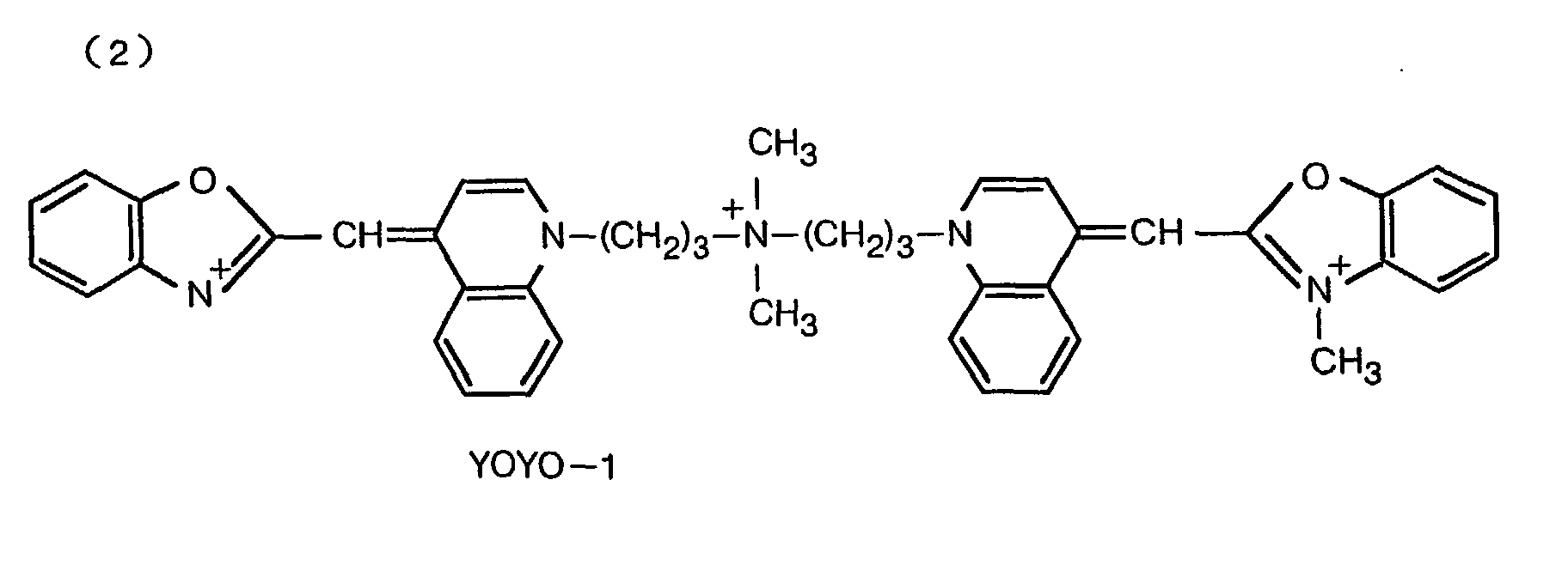
structural formula (1), YoYo-1 represented by the following
structural formula (2), ToTO-1 represented by the following
structural formula (3), Yo-Pro-1 represented by the following
structural formula (4), Cy-3® represented by the following
structural formula (5), Nile Red represented by the following
structural formula (6), BCECF represented by the following
structural formula (7), Rohdamine 6G (C. I. No. 45160),
Acridine Orange (C. I. No. 46005), SYBR Green (C2H6OS), Quantum
Red, R-Phycoerythrin, Red 613, Red 670, Fluor X,
Fluorescein-labeled amidite, FAM, AttoPhos, Bodipy
phosphatidylcholine, SNAFL, Calcium Green, Fura Red, Fluo 3,
AllPro, NBD phosphoethanolamine, and the like may be
preferably employed. When the reading light is a laser beam
of 633nm or 635nm, the fluorescent pigment may be any so long
as it can be excited by a laser beam at the wavelength. For
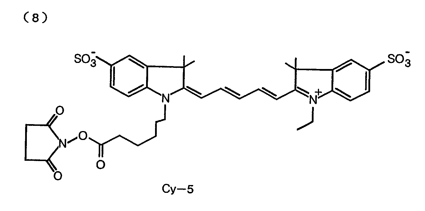
example, Cy-5® represented by the following structural formula
(8) and Allphycocyanin may be preferably employed. When the
reading light is a laser beam of 530nm or 540nm, the fluorescent
pigment may be any so long as it can be excited by a laser beam
at the wavelength. For example, Cy-3® represented by the
following structural formula (5), Rohdamine 6G (C. I. No.
45160), Rohdamine B (C. I. No. 45170), Ethidium Bromide
represented by the following structural formula (9) , Texas Red
represented by the following structural formula (10),
Propidium Iodide represented by the following structural
formula (11), POP-3 represented by the following structural
formula (12), Red 613, Red 670, Cardoxyrohdamine (R6G),
R-Phycoerythrin, Quantum Red, JOE, HEX, Ethidium homodimer,
Lissamine rhodamine B peptide and the like may be preferably
employed.
structural formula (1) ∼(12)
For example, the reading light projecting means may be
a line irradiation type light beam projecting means comprising
a combination of a slit and a fluorescent lamp or a cold cathode
fluorescent lamp or a combination of an optical system such
as a cylindrical lens and a light source such as an LED array,
an LD array or a broad area laser as well as a point scan type
light beam projecting means comprising a light source such as
an LED and a light beam scanning optical system such as a
polygonal mirror.
It is possible to provide a plurality of reading light
projecting means which emit light of different wavelengths so
that one of the reading light projecting means is selectively
employed according to the kind of image-bearing medium to be
used.
It is preferred that the length of the portion of the
image-bearing medium exposed to the reading light in the main
scanning direction be not smaller than the width of the
image-bearing medium.
The erecting unit optical system may be, for instance,
a refractive index profile type lens array such as a SELFOC®
lens array or a rod lens array, which is formed by an imaging
system where the object plane and the image plane are in one
to one correspondence, a cylindrical lens, a biaxial lens, an
aspheric lens array (see, Japanese Unexamined Patent
Publication No. 6(1994)-208081) a slit or fiber optics.
The reading light projecting means and the image-bearing
light detecting means may be disposed either on the same side
of the image-bearing medium sheet or on opposite sides of the
sheet. However, in the latter case, the support sheet and the
like of the image-bearing medium sheet should be permeable to
the image-bearing light.
When each of the first and second sensors is provided
with effective areas, where the sensor can detect light, and
noneffective areas, where the sensor cannot detect light,
which are alternately arranged in the main scanning direction,
for example, the part of the image-bearing light led by the
first optical elements is caused to impinge upon the effective
areas of the first sensor and the part of the image-bearing
light led by the second optical elements is caused to impinge
upon the effective areas of the second sensor.
When each of the first and second sensors comprises a
plurality of sensor chips, each comprising a plurality of
photoelectric convertor elements linearly arranged in a row,
arranged end to end, the central areas of the respective sensor
chips where the photoelectric convertor elements exist are the
effective areas and the end portions of the respective sensor
chips where no photoelectric convertor element exists are the
noneffective areas.
In the image information read-out apparatus of the
present invention, it is preferred that the first and second
sensors are disposed so that the effective areas of the first
and second sensors overlap each other in the main scanning
direction at portions corresponding to boundaries between the
first and second optical elements of the optical element array
and there is provided pixel signal adder means which adds up
pixel by pixel outputs of the first and second sensors for each
pixel in the portions corresponding to boundaries between the
first and second optical elements of the optical element array.
The boundary between the first and second optical elements of
the optical element array as said here need not necessarily
have only one pixel width in the main scanning but may have
a multiple pixel width. That is, the boundary may be
represented by a plurality of pixels near to pixels which form
an exact boundary.
The optical element array may be formed by either first
and second optical elements one of which transmits the
image-bearing light and the other of which reflects the same,
or first and second optical elements which reflect the
image-bearing light in different directions.
It is preferred that the optical element array itself
has a function of cutting the reading light. For example, this
may be realized by forming the optical element array itself
of a material which absorbs light at the wavelength of the
reading light or by disposing an interference filter, which
transmits the image-bearing light but does not transmit the
reading light, in front of the light incident face of the
optical element array.
When the first and second optical elements are arranged
to reflect the image-bearing light in different directions,
the optical element array may be given a function of cutting
the reading light by forming the reflecting surfaces of the
first and second optical elements by dichroic mirrors which
reflect the image-bearing light but transmit the reading
light.
A reading light cut filter which transmits the
image-bearing light but does not transmit the reading light
(e.g., a sharp cut filter or a band pass filter) may be provided
between the image-bearing medium and the line sensor.
The image information read-out apparatus of the present
invention may be provided with a plurality of sets of
image-bearing light detecting means. In this case, it is
preferred that the optical element arrays be arranged so that
the boundaries between first and second optical elements are
positioned in different positions, image-bearing light
detecting means by image-bearing light detecting means as seen
in the main scanning direction.
In the image information read-out apparatus of the
present invention where the image-bearing light detecting
means has an optical element array formed by a plurality of
first and second optical elements which are alternately
arranged and lead light in different directions, and first and
second sensors which receive light led by the first and second
optical elements, the image-bearing light emitted from the
part of the image-bearing medium exposed to the reading light
is uniformly detected by the line sensor over the entire width
of the image-bearing medium.
Even if each sensor has effective areas and noneffective
areas alternately arranged in the main scanning direction,
when such an optical element array and a pair of sensors are
employed, the image-bearing light emitted from portions
corresponding to noneffective areas of one of the sensors can
be detected by the effective areas of the other sensor, whereby
the image-bearing light entering the erecting unit optical
system can be uniformly detected over the entire width of the
image-bearing medium, and at the same time, generation of
artifact can be suppressed as compared with when only one set
of stimulated emission detecting means is employed.
When the first and second sensors are disposed so that
the effective areas of the first and second sensors overlap
each other in the main scanning direction at portions
corresponding to boundaries between the first and second
optical elements of the optical element array and there is
provided pixel signal adder means which adds up pixel by pixel
outputs of the first and second sensors for each pixel in the
portions corresponding to boundaries between the first and
second optical elements of the optical element array, even if
the image-bearing light from the portions of the image-bearing
medium corresponding to the boundaries is detected partly by
the first sensor and partly by the second sensor, the whole
image-bearing light from the portions can be detected under
substantially the same condition as other portions by adding
the outputs of the first and second sensors, whereby
discontinuity of the data at boundaries of the optical elements
can be detected and a smooth image suppressed with artifact
can be obtained.
When the optical element array itself has a function of
cutting the reading light, the reading light can be prevented
from impinging upon the line sensor without additionally
providing a reading light cut filter.
Further when a plurality of sets of image-bearing light
detecting means are provided, light collecting efficiency is
enhanced and an image higher in S/N can be obtained, whereby,
for instance, image diagnosis can be performed at a higher
reliability.
Further, when a stimulable phosphor sheet which is
anisotropic and radiates the stimulated emission in a
direction at a predetermined angle to the direction of
thickness of the stimulable phosphor sheet is employed as the
image-bearing medium and the stimulated emission detecting
means (the image-bearing light detecting means) is arranged
so that the stimulated emission incident face of the erecting
unit optical system is positioned in perpendicular to the
direction at the predetermined angle to the direction of
thickness of the stimulable phosphor sheet, the stimulated
emission can be detected more efficiently and an image further
higher in S/N can be obtained.
BRIEF DESCRIPTION OF THE DRAWINGS
Figure 1 is a schematic perspective view showing a part
of a radiation image information read-out apparatus in
accordance with an embodiment of the present invention,
Figure 2 is a cross-sectional view taken along line I-I
in Figure 1,
Figure 3 is a schematic view showing one of the sensors
forming the line sensor employed in the radiation image
information read-out apparatus shown in Figure 1,
Figure 4 is a fragmentary view showing in detail a part
of the sensor shown in Figure 3,
Figure 5 is a perspective view showing the optical
element array employed in the radiation image information
read-out apparatus shown in Figure 1,
Figure 6 is a view for illustrating the arrangement of
the line sensor and the optical element array employed in the
radiation image information read-out apparatus shown in Figure
1,
Figure 7 is a perspective view showing a modification
of the optical element array,
Figure 8 is a schematic cross-sectional view showing a
structure of a stimulated emission detecting means provided
with the optical element array shown in Figure 7,
Figure 9 is a perspective view showing another
modification of the optical element array,
Figure 10 is a schematic perspective view showing a part
of a radiation image information read-out apparatus in
accordance with another embodiment of the present invention,
Figure 11 is a cross-sectional view taken along line I-I
in Figure 10,
Figure 12 is a view for illustrating the arrangement of
the line sensor and the optical element array employed in the
radiation image information read-out apparatus shown in Figure
10,
Figure 13 is a fragmentary view showing a stimulable
phosphor sheet suitable for radiation image information
read-out apparatuses of the present invention,
Figure 14 is a perspective view showing a biaxial lens,
and
Figure 15 is a perspective view showing an aspheric lens
array.
DESCRIPTION OF THE PREFERRED EMBODIMENTS
In Figures 1 and 2, a radiation image information
read-out apparatus in accordance with an embodiment of the
present invention comprises a sub-scanning belt 5 which
conveys a stimulable phosphor sheet 1 storing thereon
radiation image information in the direction of arrow Y (the
sub-scanning direction), a stimulating light beam projecting
means, a stimulated emission detecting means, and a signal
processing means 50. The stimulating light beam projecting
means comprises a broad area laser 11 which emits a secondary
stimulating light beam L in perpendicular to the surface of
the stimulable phosphor sheet 1 and an optical system 12 which
is formed by a combination of a collimator lens which condenses
the stimulating light beam L emitted from the broad area laser
11 and a toric lens which spreads the light beam only in one
direction and causes the stimulating light beam L to impinge
upon the surface of the stimulable phosphor sheet 1 in a pattern
of a line. The stimulated emission detecting means comprises
a refractive index profile type lens array 16 (an array of a
plurality of refractive index profile type lenses such as a
SELFOC lens array) which converges stimulated emission M
emitted from the part of the stimulable phosphor sheet 1 exposed
to the line stimulating light beam L onto a line sensor 20 to
be described later, an optical element array 30 which receives
the stimulated emission M passing through the lens array 16
and divides the stimulated emission M into first and second
parts, and line sensor 20 consisting of a first sensor section
20A which receives the first part of the stimulated emission
M and converts the amount of the first part of the stimulated
emission M to a first electric signal and a second sensor
section 20B which receives the second part of the stimulated
emission M and converts the amount of the second part of the
stimulated emission M to a second electric signal. The signal
processing means 50 processes the first and second electric
signals respectively output from the first and second sensor
sections 20A and 20B of the line sensor 20. The optical element
array 30 is formed of a material which cuts the stimulating
light L.
The lens array 16 and the optical element array 30 are
disposed so that the stimulated emission emitted from the part
of the stimulable phosphor sheet 1 exposed to the line
stimulating light beam L is uniformly received by the line
sensor 20 over the entire width of the stimulable phosphor sheet
1.
The lens array 16 forms an erecting unit optical system
and forms an image of the stimulated emission M on the light
receiving face of each of the first and second sensor sections
20A and 20B in a natural size.
As shown in Figures 3 and 4, each of the sensor sections
20A (20B) comprises a plurality of sensor chips 21A (21B)
arranged in a row in the direction of arrow X (the main scanning
direction) . The hatched portion 24A (24B) in each sensor chip
21A (21B) is an effective area which can sense light. In more
detail, as shown in Figure 4, the effective area 24A (24B)
comprises an array of photoelectric convertor elements 22
extending in the main scanning direction, and the sensor chip
21A (21B) has noneffective areas on opposite ends of the
effective area 24A (24B). The sensor section 20A (20B) is
formed by connecting a plurality of such sensor chips 21A (21B)
end to end, and accordingly, in the sensor section 20A (20B),
the effective areas 24A (24B) and the noneffective areas 25A
(25B) are alternately arranged in the main scanning direction
X. The senor chip 21A (21B) may be, for instance, an amorphous
silicone sensor, a CCD sensor or a MOS image sensor.
As shown in Figure 5, the optical element array 30
comprises a plurality of first optical elements 31 which
transmit the stimulated emission M and a plurality of second
optical elements 33 each having a reflecting surface which
reflects the stimulated emission M so that each of the first
optical elements 31 leads the stimulated emission to the first
sensor section 20A and each of the second optical elements 33
leads the stimulated emission to the second sensor section 20B,
the first and second optical elements 31 and 33 being
alternately arranged in the main scanning direction X. The
first and second sensor sections 20A and 20B are disposed with
their respective effective areas 24A and 24B positioned to
receive the stimulated emission led by the first and second
optical elements 31 and 33, respectively.
Figure 6 shows in more detail arrangement of the optical
element array 30 relative to the first and second sensor
sections 20A and 20B. In Figure 6, arrows shown in the optical
element array 30 indicate direction of travel of the stimulated
emission M passing through the respective optical elements.
That is, the first optical elements 31 lead the stimulated
emission M to the first sensor section 20A and the second
optical elements 33 lead the same to the second sensor section
20B. As described above, the first and second sensor sections
20A and 20B are disposed with their respective effective areas
24A and 24B positioned to receive the stimulated emission led
by the first and second optical elements 31 and 33, respectively.
Accordingly, the noneffective areas 25A of the first sensor
section 20A and the noneffective areas 25B of the second sensor
section 20B are alternately arranged in the main scanning
direction X. With this arrangement, the parts of the
stimulated emission M emitted from portions 40 of the
stimulable phosphor sheet 1 corresponding to the noneffective
areas of one of the sensor sections can be led to the effective
areas of the other sensor section.
Further, the first and second sensor sections 20A and
20B are positioned so that the effective areas 24A of the first
sensor section 20A partly overlap with the effective areas 24B
of the first sensor section 20B in the main scanning direction
X at parts corresponding to boundaries 35 between the first
optical elements 31 and the second optical elements 33 of the
optical element array 30.
The signal processing means 50 is provided with a pixel
signal adder mean 51 and adds up the pixel signals, pixel by
pixel, detected by the part of the effective areas 24A of the
first sensor section 20A and the part of the effective areas
24B of the second sensor section 20B which overlap each other.
The operation of the radiation image information
read-out apparatus of this embodiment will be described
hereinbelow. The sub-scanning belt 5 conveys a stimulable
phosphor sheet 1 storing thereon radiation image information
in the sub-scanning direction Y at a constant speed. At the
same time, a stimulating light beam L emitted from the broad
area laser 11 is converted to a parallel beam by the optical
system 12 comprising the collimator lens and the toric lens
and is projected onto the stimulable phosphor sheet 1 to
irradiate a line-like portion extending in the main scanning
direction X over the entire width of the stimulable phosphor
sheet 1.
The line-like irradiated portion of the stimulable
phosphor sheet 1 exposed to the stimulating light beam L emits
stimulated emission M in an amount proportional to the amount
of radiation energy stored therein.
The stimulated emission M is led to the first and second
sensor sections 20A and 20B of the line sensor 20 by the lens
array 16 and the optical element array 30 and is
photoelectrically detected by the first and second sensor
sections 20A and 20B. Though the stimulated emission M
reflected at the surface of the stimulable phosphor sheet 1
is in the stimulated emission M passing through the lens array
16 in a slight amount, such stimulated emission M is cut by
the stimulating light cut filter of the optical element array
30 and cannot impinge upon the sensor sections 20A and 20B.
Each photoelectric convertor elements 22 first and second
sensor sections 20A and 20B converts the amount of the
stimulated emission M (representing the radiation image
information) into an analog electric signal S. The light
detecting signal (analog electric signal) S is amplified and
digitized by the signal processing means 50, and a digital image
signal thus obtained is output to an image processor. The
digital image signal is subjected to gradation processing and
the like by the image processor and used to reproduce the
radiation image recorded on the stimulable phosphor sheet 1.
Since the noneffective areas 25A of the first sensor
section 20A and the noneffective areas 25B of the second sensor
section 20B are alternately arranged in the main scanning
direction X along the line-like irradiated portion 40 of the
stimulable phosphor sheet 1 as shown in Figure 6, the stimulated
emission M emitted from the points in the irradiated portion
40 corresponding to the noneffective areas 25A of the first
sensor section 20A is detected by the sensor chips 21B of the
second sensor section 20B and the stimulated emission M emitted
from the points in the irradiated portion 40 corresponding to
the noneffective areas 25B of the second sensor section 20B
is detected by the sensor chips 21A of the first sensor section
20A. The stimulated emission M emitted from the portion of
the stimulable phosphor sheet 1 corresponding to the
boundaries 35 between the first optical elements 31 and the
second optical elements 33 of the optical element array 30
partly impinges upon one of the first and second optical
elements 31 and 33 and partly impinges upon the other optical
element and accordingly, is partly detected by one of the first
and second sensor sections 20A and 20B and is partly detected
by the other sensor section. However by adding the signals
from the respective sensor sections 20A and 20B for each pixel
by the pixel signal adder means 51 of the signal processing
means 50, the stimulated emission M can be detected uniformly
over all the pixels in irradiated portion 40 on the stimulable
phosphor sheet 1.
Though, in the embodiment described above, the first
optical elements 31 of the optical element array 30 transmits
the stimulated emission M whereas the second optical elements
33 of the optical element array 30 reflects the same, the
optical elements array 30 may be formed by first and second
optical elements which both reflect the stimulated emission
M. Figure 7 shows an example of such an optical element array.
The optical element array 60 shown in Figure 7 comprises a
plurality of first and second optical elements 62 and 64 which
are alternately arranged in the main scanning direction X.
Each of the first optical elements 62 has a reflecting surface
61 which reflects the stimulated emission M in a first direction,
whereas each of the second optical elements 64 has a reflecting
surface 63 which reflects the stimulated emission M in a second
direction opposite to the first direction.
Figure 8 is a fragmentary cross-sectional showing a
radiation image information read-out apparatus employing the
optical element array 60 shown in Figure 7. As shown in Figure
8, in this case, the first and second sensor sections 20A and
20B are symmetrically disposed on opposite sides of the optical
element array 60. The stimulated emission M is divided into
two parts by the optical element array 60, one of the two parts
reflected to impinge upon the first sensor section 20A and the
other reflected to impinge upon the second sensor section 20B.
It is preferred that the optical element array 60 doubles
as a stimulating light cut filter. For example, the optical
element array 60 may be formed by a material which absorbs the
stimulating light beam L or each of the reflecting surface 61
and 63 of the first and second optical elements 62 and 64 may
be formed as a dichroic mirror which reflects the stimulated
emission M and transmits the stimulating light beam L.
Further, when the optical element array is formed by
first and second optical elements 71 and 72 both having a
reflecting surfaces, it is preferred that the reflecting
surfaces of the first and second optical elements 71 and 72
partly overlap (75) each other in the main scanning direction
at the boundaries between the reflecting surfaces of the first
and second optical elements 71 and 72 as shown in Figure 9.
Without such overlapping portions 75, parts of the stimulated
emission M impinging upon the boundaries go through the optical
element array and can be received by neither the first sensor
section 20A nor the second sensor section 20B. By providing
such overlapping portions 75, the stimulated emission M
emitted over the entire width of the stimulable phosphor sheet
1 in the main scanning direction can be detected.
Further, though, in the embodiments described above, the
stimulated emission M is detected by a single set of stimulated
emission detecting means, the stimulated emission M may be
detected by the use of two or more sets of stimulated emission
detecting means.
Now a radiation image information read-out apparatus in
accordance with another embodiment of the present invention,
where the stimulated emission M is detected by the use of two
or more sets of stimulated emission detecting means will be
described with reference to Figures 10 to 13, hereinbelow.
The radiation image information read-out apparatus of
this embodiment differs from that of the preceding embodiment
only in that an additional (second) stimulated emission
detecting means is provided and accordingly the elements
analogous to those in the preceding embodiments are given the
same reference numerals and will not be described here. That
is, the radiation image information read-out apparatus of this
embodiment is further provided with a second stimulated
emission detecting system comprising a refractive index
profile type lens array 16' which converges stimulated
emission M emitted from the part of the stimulable phosphor
sheet 1 exposed to the line stimulating light beam L onto a
line sensor 20', an optical element array 30' which receives
the stimulated emission M passing through the lens array 16'
through a stimulating light cut filter (not shown) which cuts
the stimulating light L in the stimulated emission M passing
through the lens array 16' and divides the stimulated emission
M into first and second parts, and the line sensor 20'
consisting of a first sensor section 20A' which receives the
first part of the stimulated emission M and converts the amount
of the first part of the stimulated emission M to a first
electric signal and a second sensor section 20B' which receives
the second part of the stimulated emission M and converts the
amount of the second part of the stimulated emission M to a
second electric signal. In place of the signal processing
means 50 which processes the electric signals respectively
output from the first and second sensor sections 20A and 20B
of the line sensor 20, a signal processing means 80 which
processes the electric signals respectively output from the
first and second sensor sections 20A and 20B of the first line
sensor 20 and the first and second sensor sections 20A' and
20B' of the second line sensor 20' is provided.
As shown in Figure 12, the sensor chips 21A, 21B, 21A',
and 21B' are arranged so that their noneffective areas 25A,
25B, 25A' and 25B' are positioned in different positions in
the main scanning direction X and the parts of the stimulated
emission M emitted from portions 40 of the stimulable phosphor
sheet 1 corresponding to the noneffective areas of one of the
sensor sections can be led to the effective areas of another
sensor section. Further, the first and second optical element
arrays 30 and 30A' are arranged so that the boundaries 35
between first and second optical elements in the first optical
element array 30 are positioned in different positions from
those 35' in the second optical element array 30' as seen in
the main scanning direction, thereby suppressing
discontinuity in data which can be caused near the boundaries
of the optical elements.
The signal processing means 80 is provided with a pixel
signal adder mean 81 and adds up the pixel signals, pixel by
pixel, detected by the sensor sections 20A, 20B, 20A' and 20B'
with the respective pixel signals multiplied by predetermined
coefficients. Accordingly, data is prevented from being
discontinuous at the noneffective areas 25A, 25B, 25A' and 25B'
or the boundaries between optical elements in the optical
element arrays 30 and 30', which results in a smooth image
suppressed with artifact.
Further, since the first and second optical element
arrays 30 and 30A' are arranged so that the boundaries 35
between optical elements in the first optical element array
30 are positioned in different positions from those 35' in the
second optical element array 30' as seen in the main scanning
direction, discontinuity in data which can be caused near the
boundaries of the optical elements can be suppressed, whereby
the stimulated emission M can be detected more uniformly over
all the pixels in irradiated portion 40 on the stimulable
phosphor sheet 1.
Further when a two sets of stimulated emission detecting
means are provided, light collecting efficiency is enhanced
and an image higher in S/N can be obtained as compared with
when only one set of stimulated emission detecting means is
employed.
Though the stimulating light beam L need not be
necessarily caused to impinge upon the stimulable phosphor
sheet 1 in substantially perpendicular to the surface of the
stimulable phosphor sheet 1 as in the embodiments described
above, it is preferred that the optical system and the line
sensor be disposed taking into account the light collecting
efficiency when the stimulating light beam L is caused to
obliquely impinge upon the surface of the stimulable phosphor
sheet 1.
In the radiation image information read-out apparatus
of this invention, it is especially preferred that the
stimulable phosphor sheet be anisotropic. Figure 13 shows an
example of such an anisotropic stimulable phosphor sheet. The
stimulable phosphor sheet 60 of this example comprises a
support sheet 61 and a stimulable phosphor layer 62 formed on
the support sheet 61. The stimulable phosphor layer 62 is
partitioned into lots of fine cells by partitions 63 which are
disposed at a predetermined angle α to the direction of
thickness of the stimulable phosphor sheet 60 and reflect the
stimulated emission M. When the stimulable phosphor sheet 60
with such a structure is employed, the stimulated emission M
emitted from the portion of the stimulable phosphor sheet 60
exposed to the stimulating light beam L travels toward the
surface of the stimulable phosphor sheet 60 repeatedly
reflected by adjacent two partitions 63 and accordingly
emanates from the stimulable phosphor sheet 60 without largely
deviating from the direction in which the partitions 63 extend
(the direction of anisotropy). Accordingly, by positioning
the stimulated emission incident face 17 of the lens array 16
in perpendicular to the direction of anisotropy, the
stimulated emission M is efficiently collected to the
stimulated emission incident face 17, whereby the stimulated
emission detecting efficiency can be enhanced and a high
quality radiation image can be reproduced.
An anisotropic stimulable phosphor sheet can be also
obtained by orienting prism crystal type stimulable phosphor
so that the crystals are directed in the direction of thickness
of the stimulable phosphor sheet and the stimulated emission
M is repeatedly reflected between the crystal faces.
Further, in the present invention, the stimulable
phosphor sheet may be that provided with both radiation
absorbing function and radiation energy storing function or
that provided with an energy storing phosphor layer in order
to separate radiation absorbing function and radiation energy
storing function from each other as disclosed in Japanese
Patent Application No. 11(1999)-372978. When the stimulable
phosphor sheet with an energy storing phosphor layer is
employed, detecting quantum efficiency, e.g., the radiation
absorbance efficiency, stimulated emission emitting
efficiency and stimulated emission taking out efficiency, is
increased in total, whereby the radiation image quality can
be improved.
Though, in the embodiments described above, the reading
light projecting means is a line beam projecting means, the
reading light projecting means may be of a point scan type which
causes a point-like light beam to scan the stimulable phosphor
sheet in the main scanning direction.
Further, as the lens array 16, a biaxial lens array formed
of a plurality of biaxial refractive index profile type lens
elements or an aspheric lens array may be employed in place
of the SELFOC lens. The biaxial refractive index profile type
lens element is a lens element which is a rectangular prism
in shape and whose refractive index is gradually reduced from
the center of X-axis toward the ends X1 and X2 of X-axis as
shown in Figure 14. The biaxial refractive index profile type
lens element 114a images in a different manners according to
its length d. In this embodiment, the biaxial refractive index
profile type lens element 114a forms an erecting unit optical
system in the direction of the refractive index profile axis
(X-axis). Since the biaxial refractive index profile type
lens element 114a is formed by melting a plurality of sheets
of glasses 115a, 115b, 115c ····· 115d different in refractive
index, the aperture and the refractive index difference
between the central part and the ends can be freely set. For
example, in this particular embodiment, the biaxial refractive
index profile type lens element 114a is 1.83 in maximum
refractive index nmax and 1.52 in minimum refractive index nmin.
This biaxial refractive index profile type lens element 114a
has no refractive index gradient in the direction Y-axis. That
is, the refractive index of the lens element 114a is uniform
in the direction of Y-axis. The biaxial lens array is formed
by arranging a plurality of such biaxial refractive index
profile type lens elements 114a in the direction of refractive
index profile (the direction of X-axis) . Whereas the aspheric
lens array is formed by arranging a plurality of aspheric lenses,
each of which is longer in distance L between the cylindrical
faces than the thickness d, in two rows 123 and 124 as shown
in Figure 15, and the two rows of lens arrays in which aspheric
lenses 121 of the same shape are symmetrically arranged form
an erecting unit optical system.
Though, in the embodiments described above, the present
invention is described in conjunction with a radiation image
information read-out apparatus for reading a radiation image
from a stimulable phosphor sheet, the present invention can
be applied to image reading in various systems including a
fluorescence detecting system, an auto-radiography system, an
electron microscope and a radiation diffraction detecting
system. For example, when the present invention is to be
applied to the fluorescence detecting system, reading light
having a wavelength which can cause fluorescence pigment, used
in causing the image-bearing medium to bear an image, to emit
fluorescence is employed. Further, the image information
read-out apparatus of the present invention can be employed
as a scanner for, for instance, a copier in which a line light
beam is projected onto a sheet such as a photographic film and
an image on the sheet is read out on the basis of light reflected
at the surface of the sheet.