EP1204213A1 - Mobile wireless communication device - Google Patents
Mobile wireless communication device Download PDFInfo
- Publication number
- EP1204213A1 EP1204213A1 EP00937208A EP00937208A EP1204213A1 EP 1204213 A1 EP1204213 A1 EP 1204213A1 EP 00937208 A EP00937208 A EP 00937208A EP 00937208 A EP00937208 A EP 00937208A EP 1204213 A1 EP1204213 A1 EP 1204213A1
- Authority
- EP
- European Patent Office
- Prior art keywords
- unit
- power supply
- bias
- control signal
- supply voltage
- Prior art date
- Legal status (The legal status is an assumption and is not a legal conclusion. Google has not performed a legal analysis and makes no representation as to the accuracy of the status listed.)
- Withdrawn
Links
Images




Classifications
-
- H—ELECTRICITY
- H04—ELECTRIC COMMUNICATION TECHNIQUE
- H04B—TRANSMISSION
- H04B1/00—Details of transmission systems, not covered by a single one of groups H04B3/00 - H04B13/00; Details of transmission systems not characterised by the medium used for transmission
- H04B1/06—Receivers
- H04B1/10—Means associated with receiver for limiting or suppressing noise or interference
- H04B1/1027—Means associated with receiver for limiting or suppressing noise or interference assessing signal quality or detecting noise/interference for the received signal
-
- H—ELECTRICITY
- H04—ELECTRIC COMMUNICATION TECHNIQUE
- H04W—WIRELESS COMMUNICATION NETWORKS
- H04W52/00—Power management, e.g. Transmission Power Control [TPC] or power classes
- H04W52/02—Power saving arrangements
- H04W52/0209—Power saving arrangements in terminal devices
- H04W52/0225—Power saving arrangements in terminal devices using monitoring of external events, e.g. the presence of a signal
- H04W52/0245—Power saving arrangements in terminal devices using monitoring of external events, e.g. the presence of a signal according to signal strength
-
- Y—GENERAL TAGGING OF NEW TECHNOLOGICAL DEVELOPMENTS; GENERAL TAGGING OF CROSS-SECTIONAL TECHNOLOGIES SPANNING OVER SEVERAL SECTIONS OF THE IPC; TECHNICAL SUBJECTS COVERED BY FORMER USPC CROSS-REFERENCE ART COLLECTIONS [XRACs] AND DIGESTS
- Y02—TECHNOLOGIES OR APPLICATIONS FOR MITIGATION OR ADAPTATION AGAINST CLIMATE CHANGE
- Y02D—CLIMATE CHANGE MITIGATION TECHNOLOGIES IN INFORMATION AND COMMUNICATION TECHNOLOGIES [ICT], I.E. INFORMATION AND COMMUNICATION TECHNOLOGIES AIMING AT THE REDUCTION OF THEIR OWN ENERGY USE
- Y02D30/00—Reducing energy consumption in communication networks
- Y02D30/70—Reducing energy consumption in communication networks in wireless communication networks
Definitions
- This invention is related to a mobile radio communication device such as a mobile telephone, and particularly to a mobile radio communication device in which the current consumption is reduced.
- Fig. 1 is a block diagram showing a construction of the conventional mobile radio communication device such as a mobile telephone, and generally a mobile radio communication device comprises, as shown in the figure, an antenna 1, a radio section 2, a control section 3, and a fixed-voltage power supply unit 41.
- the radio section 2 consists of an antenna sharing unit 5, a receiver unit 6, a transmitter unit 7, and a synthesizer unit 8, and the current consumption of the mobile radio communication device is reduced by turning ON/OFF the fixed power supply voltage output from the fixed-voltage power supply unit 41, as needed, by means of the ON/OFF control signal 102 from the control section 3. Further, there is also the one in which, at the time of reception, the gain of the amplifier in the receiver unit 6 is variably controlled by a gain control signal 101 from the control section 3.
- the power supply voltage needs to be kept ON for a long time for portions which require a certain time for its stabilization since the turning ON of the power supply voltage, and in a mobile radio communication device which performs an intermittent operation such as the time division multiple access, if the intermittent operation interval is short, it is also needed to keep the power supply voltage ON for a long time, so there was a problem that the current consumption could not fully be reduced.
- Fig. 2 is a block diagram showing a conventional mobile radio communication device having a variable-voltage power supply section, and it includes a variable-voltage power supply unit 42 which varies the output power supply voltage according to a voltage control signal 103 from the control section 3, and a method is employed in which variable control of the power supply voltage of the receiver unit 6 is carried out within the range of enabling the receiving quality to be maintained, thereby to reduce the current in the receiver unit 6.
- the power supply voltage is controlled also in the receive state, but there was a problem that it is less effective as compared with the method in which the gain of the amplifier or the like in the receiver unit 6 is controlled according to the receive field strength, and there was a further problem that it is unclear whether or not the receiving quality can be maintained for a rapid change in the receive field strength.
- This invention has been accomplished to solve the above problems, aiming at obtaining a mobile radio communication device in which the current consumption can be reduced, with a simple construction and control, in portions requiring no full performance during operation.
- the mobile radio communication device related to this invention comprises: a receiver unit for receiving transmitted radio waves; a synthesizer unit for outputting a local oscillation signal by which the receiver unit carries out a frequency conversion; a variable-voltage power supply unit for supplying to the receiver unit and the synthesizer unit a first power supply voltage that is the power supply voltage for normal operation, or a second power supply voltage lower than the first power supply voltage, provided that those units operate; a control signal processing unit for outputting a voltage control signal by which the variable-voltage power supply unit outputs the first power supply voltage or the second power supply voltage; a field strength detecting unit for detecting the received field strength when the receiver unit receives radio waves; and a memory for previously storing a gain difference between the gain at the detection of the receive field strength when the power supply voltage supplied from the variable-voltage power supply unit to the receiver unit and the synthesizer unit is the first power supply voltage and that when the above power supply voltage is the second power supply voltage; in which, when the field strength detecting unit detects the
- This provides an advantage that the current consumption in portions requiring no full performance can be reduced in a mode other than the receive operation or the transmit operation.
- the power supply voltage supplied from the variable-voltage power supply unit to the synthesizer unit is set to the second power supply voltage by a voltage control signal output from the control signal processing unit, and at the time of reception, the power supply voltage supplied from the variable-voltage power supply unit to the synthesizer unit is set to the first power supply voltage by the voltage control signal output from the control signal processing unit.
- the power supply voltage of the receiver unit is turned OFF except for reception, and to start reception, the power supply voltage supplied from the variable-voltage power supply unit to the receiver unit is set, before reception, to the second power supply voltage by the voltage control signal output from the control signal processing unit, and the power supply voltage supplied from the variable-voltage power supply unit to the receiver unit is set, just before reception, to the first power supply voltage by the voltage control signal output from the control signal processing unit.
- the mobile radio communication device related to this invention includes a transmitter unit for transmitting a radio wave, and in which the power supply voltage of the transmitter unit is turned OFF except for transmission, and to start transmission, the power supply voltage supplied from the variable-voltage power supply unit to the transmitter unit is set, before transmission, to the second power supply voltage by the voltage control signal that is output by the control signal processing unit, and the power supply voltage supplied from the variable-voltage power supply unit to the transmitter unit is set, just before transmission, to the first power supply voltage by the voltage control signal output from the control signal processing unit.
- the mobile radio communication device related to this invention comprises: a receiver unit for receiving transmitted radio waves; a synthesizer unit for outputting a local oscillation signal by which the receiver unit carries out a frequency conversion; a variable bias unit for supplying to the receiver unit and the synthesizer unit a first bias that is the bias for the normal operation, or a second bias that is lower than the first bias, provided that those units operate; a control signal processing unit for outputting a bias control signal by which the variable bias unit outputs the first bias or the second bias; a field strength detecting unit for detecting the received field strength when the receiver unit receives radio waves; and a memory for previously storing a gain difference between the gain at the detection of the received field strength when the bias supplied from the variable bias unit to the receiver unit and the synthesizer unit is the first bias and that when the above bias is the second bias; in which, when the field strength detecting unit detects the receive field strength, the bias to be supplied from the variable bias unit to the receiver unit and the synthesizer unit is set to the
- This provides an advantage that the current consumption in portions requiring no full performance except for the receive operation or the transmit operation can be reduced.
- the bias supplied from the variable bias unit to the synthesizer unit is set to the second bias by the bias control signal output from the control signal processing unit, and at the time of reception, the bias supplied from the variable bias unit to the synthesizer unit is set to the first bias by the bias control signal output from the control signal processing unit.
- the power supply voltage of the receiver unit is turned OFF except for reception, and to start reception, the bias supplied from the variable bias unit to the receiver unit is set, before reception, to the second bias by the bias control signal is output from the control signal processing unit, and the bias supplied from the variable bias unit to the receiver unit is set, just before reception, to the first bias by the bias control signal output from the control signal processing unit.
- the mobile radio communication device related to this invention includes a transmitter unit for transmitting a radio wave, and in which the power supply voltage of the transmitter unit is turned OFF except for transmission, and to start transmission, the bias supplied from the variable bias unit to the transmitter unit is set, before transmission, to the second bias by the bias control signal output from the control signal processing unit, and the bias supplied from the variable bias unit to the transmitter unit is set, just before transmission, to the first bias by the bias control signal output from the control signal processing unit.
- the mobile radio communication device related to this invention comprises: a receiver unit for receiving transmitted radio waves; a synthesizer unit for outputting a local oscillation signal by which the receiver unit carries out a frequency conversion; a variable-voltage power supply unit for supplying to the receiver unit and the synthesizer unit a first power supply voltage that is the power supply voltage for normal operation, or a second power supply voltage that is lower than the first power supply voltage, provided that those units operate; a variable bias unit for supplying to the receiver unit and the synthesizer unit a first bias that is the bias for the normal operation, or a second bias that is lower than the first bias, provided that those units operate; a control signal processing unit for outputting a voltage control signal by which the variable-voltage power supply unit outputs the first power supply voltage or the second power supply voltage, and by which the variable bias unit outputs the first bias or the second bias, a field strength detecting unit for detecting the received field strength when the receiver unit receives radio waves; and a memory for previously storing a gain difference between
- This provides an advantage that the current consumption in portions requiring no full performance except for the receive operation or the transmit operation can be reduced.
- the power supply voltage supplied from the variable-voltage power supply unit to the synthesizer unit is set to the second power supply voltage by a voltage control signal output from the control signal processing unit, while the bias supplied from the variable bias unit to the synthesizer unit is set to the second bias by a bias control signal output from the control signal processing unit, and at the time of reception, the power supply voltage supplied from the variable-voltage power supply unit to the synthesizer unit is set to the first power supply voltage by the voltage control signal output from the control signal processing unit, while the bias supplied from the variable bias unit to the synthesizer unit is set to the first bias by the bias control signal that is output by the control signal processing unit.
- the power supply voltage of the receiver unit is turned OFF except for reception, and to start reception, before reception, the power supply voltage supplied from the variable-voltage power supply unit to the receiver unit is set to the second power supply voltage by the voltage control signal output from the control signal processing unit, while the bias supplied from the variable bias unit to the receiver unit is set to the second bias by the bias control signal output from the control signal processing unit, and just before reception, the power supply voltage supplied from the variable-voltage power supply unit to the receiver unit is set to the first power supply voltage by the voltage control signal output from the control signal processing unit, while the bias supplied from the variable bias unit to the receiver unit is set to the first bias by the bias control signal output from the control signal processing unit.
- the mobile radio communication device related to this invention includes a transmitter unit for transmitting a radio wave, and in which the power supply voltage of the transmitter unit is turned OFF except for transmission, and to start transmission, before transmission, the power supply voltage supplied from the variable-voltage unit to the transmitter unit is set to the second power supply voltage by the voltage control signal output from the control signal processing unit, while the bias supplied from the variable bias unit to the transmitter unit is set to the second bias by the bias control signal output from the control signal processing unit, and just before transmission, the power supply voltage supplied from the variable-voltage power supply unit to the transmitter unit is set to the first power supply voltage by the voltage control signal output from the control signal processing unit, while the bias supplied from the variable bias unit to the transmitter unit is set to the first bias by the bias control signal output from the control signal processing unit.
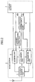
- Fig. 3 is a block diagram showing the construction of the mobile radio communication device according to the first embodiment for carrying out this invention.
- description is made, for instance, to a mobile radio communication device using the time division multiple access (hereinafter referred to as TDMA), one of the mobile communication access systems for digital mobile telephone or the like.
- TDMA time division multiple access
- a mobile radio communication device comprises an antenna 1, a radio section 2, a control section 3 and a power supply section 4; wherein the radio section 2 consists of an antenna sharing unit 5, a receiver unit 6, a transmitter unit 7 and a synthesizer unit 8; the receiver unit 6 consists of a high-frequency amplifier 61, a frequency mixer 62, an intermediate frequency amplifier 63, and a demodulator 64; and the synthesizer unit 8 consists of a.local oscillator 81, and a PLL 82.
- control section 3 is made up of a received data processing unit 31 for processing demodulated received data, a field strength detecting unit 32 for detecting receive field strength, a control signal processing unit 33 for outputting a gain control signal 101, an ON/OFF control signal 102 and a voltage control signal 103, and a memory 34 for previously storing a gain difference between the gain at the detection of received field strength when the power supply voltage of the receiver unit 6 and the synthesizer unit 8 is a power supply voltage for normal operation and the gain at the detection of receive field strength when the above power supply voltage being a power supply voltage lower than the power supply voltage for normal operation.
- the power supply section 4 consists of a fixed-voltage power supply unit 41 which is controlled by the ON/OFF control signal 103 from the control signal processing unit 33 for generating a fixed voltage, and a variable-voltage power supply unit 42, which outputs a power supply voltage VH (first power supply voltage) for normal operation and a power supply voltage VL (second power supply voltage) lower than the power supply voltage VH for normal operation according to the voltage control signal 103 from the control signal processing unit 33.
- VH first power supply voltage
- VL second power supply voltage
- a radio wave sent from a base station (not shown) is received at the antenna 1, and the received high-frequency signal is input to the receiver unit 6 through the antenna sharing unit 5.
- the received high-frequency signal is subjected to high-frequency amplification by the high-frequency amplifier 61, and in the frequency mixer 62, it is mixed with the local oscillation signal from the local oscillator 81 in the synthesizer unit 8 and subjected to frequency conversion to an intermediate frequency signal. Further, the intermediate frequency signal is demodulated by the demodulator 64, after amplified by the intermediate frequency amplifier 63, and subjected to data processing by the received data processing unit 31.
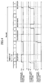
- Fig. 4 is a chart showing the power supply voltage control timing according to the first embodiment for carrying out this invention.
- the TDMA frame in the figure shows one TDMA frame construction for a telephone call in the GSM (Global System for Mobile Communications), which is a pan-European system.
- GSM Global System for Mobile Communications
- a telephone call is based on a periodical pattern, in which a receive operation (zeroth slot) and a send operation (third slot) are performed for one slot, respectively, in one frame.
- the remaining six slots are idle slots which are not related to a call, and the idle slots allow the monitoring of the receive field strength from a neighboring base station.
- the synthesizer unit 8 outputs different frequencies corresponding to the respective channels in reception, transmission, and monitoring. If the power supply voltage of the synthesizer unit 8 is once turned OFF, a certain time is required until data is set in the PLL 82 and the local oscillator 81 converges to a desired frequency after the turning ON, and thus, during a call, the power supply voltage of the synthesizer unit 8 is always put in the ON state by the ON/OFF control signal 102 from the control signal processing unit 33.
- the power supply voltage output of the variable-voltage power supply unit 42 is controlled by the voltage control signal 103 from the control signal processing unit 33 so as to be set to a power supply voltage VL lower than a power supply voltage VH for normal operation, provided that the synthesizer unit 8 operates, and supplied to the synthesizer unit 8.
- the power supply voltage of the variable-voltage power supply unit 42 is set to the power supply voltage VH for normal operation by the voltage control signal 103 and supplied to the synthesizer unit 8 a little before each slot.
- the power supply voltage of the receiver unit 6 is made ON from OFF by the ON/OFF control signal 102 before the receive slot, and it is set to the power supply voltage VL lower than the power supply voltage VH for normal operation by the voltage control signal 103 as long as the receiver unit 6 operates, and set to the power supply voltage VH for normal operation by the voltage control signal 103 just before the receive slop.
- the power supply voltage of the receiver unit 6 is made ON from OFF just before the receive slot by the ON/OFF control signal 103, and set to the power supply voltage VH for normal operation by the voltage control signal 103.
- the power supply voltage of the receiver unit 6 is set to the power supply voltage VL lower than the power supply voltage VH for normal operation by the voltage control signal 103 within the operation range of the receiver unit 6, and in idling slots other than monitoring, the power supply voltage of the receiver unit 6 is turned OFF by the ON/OFF control signal 102.
- the power supply voltage of the transmitter unit 7 In starting transmission, if the power supply voltage of the transmitter unit 7 needs to be turned ON considerably before the transmission slot for some reason, then, before the transmission slot, the power supply voltage of the transmitter unit 7 is turned ON from OFF by the ON/OFF control signal 102, and set to the power supply voltage VL lower than the power supply voltage VH for normal operation by the voltage control signal 103 as long as the transmitter unit 7 operates, and just before the transmission slot, set to the power supply voltage VH for normal operation by voltage control signal 103.
- the power supply voltage of the transmitter unit 7 is turned ON from OFF by the ON/OFF control signal 102 just before the transmission slot, and set to the power supply voltage VH for normal operation by the voltage control signal 103.
- the power supply voltage of the transmitter unit 7 is turned OFF by the ON/OFF control signal 102.
- the power supply voltage is OFF in portions in which no problem is caused by turning OFF the power supply voltage, and in portions in which the power supply voltage needs to be ON, the power supply voltage is turned ON and set to the lower power supply voltage VL within the operation range when no full performance is required, for instance, at the time of monitoring, and at the time of reception or transmission, it is set to the power supply voltage VH for normal operation, thereby to reduce the current consumption while maintaining the performance.
- the power supply voltage of the synthesizer unit 8 is set to the power supply voltage VL lower than the power supply voltage VH for normal operation by the voltage control signal 103 within the operation range of the synthesizer unit 8, while in the receive or transmit operation, the power supply voltage of the variable-voltage power supply unit 42 is set to the power supply voltage VH for normal operation by the voltage control signal 103 a little before each slot, and the power supply voltage of the synthesizer unit 8 is periodically turned OFF by the ON/OFF control signal 102 in portions where the power supply voltage can be turned OFF.
- the gain of the whole receiver unit 6 becomes lower.
- previously stored in the memory 34 is a gain difference between the gain at the detection of the receive field strength when the power supply voltage of the receiver unit 6 and the synthesizer unit 8 is the power supply voltage VH for normal operation and the gain at the detection of receive field strength when it is the power supply voltage VL lower than the power supply voltage VH for normal operation, and a CPU, not shown, in the control section 3 uses this gain difference to correct the detected receive field strength.
- the power supply voltage of the receiver unit 6 and the synthesizer unit 8 is set to the power supply voltage VH for normal operation, and monitor reception is performed. If the receive field strength is high, control is made by the gain control signal 191 from the control signal processing unit 33 so that the gain of the amplifier in the receiver unit 6 becomes low, thereby to reduce the current consumption.
- the power supply voltage of the synthesizer unit 8 in which the power supply voltage cannot periodically be turned OFF because a certain time is taken for the frequency convergence, is set to be low by the variable-voltage power supply unit 42 within its operation range, and at the time of monitoring, reception is performed after the power supply voltage is set to be lower than for normal reception by the variable-voltage power supply unit 42 as long as the receiver unit 6 operates, thereby to provide an advantage in the current consumption in portions requiring no full performance can be reduced except for the receive or transmit operation.
- the gain difference of the receiver unit 6 between the power supply voltage VH for normal operation and the low power supply voltage VL is previously stored in the memory 34, and the detected receive field strength is corrected at the time of monitoring, so the monitoring of the receive field strength can fully be performed. Further, since the power supply voltage of each unit is set to the power supply voltage VH for normal operation in the receive or transmit operation, deterioration of the speech quality is prevented.
- the present embodiment has been explained as to the case in which the application is conducted to the call by a mobile radio communication device of the TDMA system, However, the application to the monitoring of the receive field strength during standby or to a mobile radio communication device performing an intermittent operation is also possible.
- the power supply voltage is controlled separately for the receiver unit 6, transmitter unit 7, and synthesizer unit 8, but it is also possible that each unit is subdivided for separate control of the timing and power supply voltage; for instance, the synthesizer unit 8 is subdivided into the local oscillator 81 and the PLL 82, and the receiver unit 6 is subdivided into the high-frequency amplifier 61, the frequency mixer 62, the intermediate frequency amplifier 63, and the demodulator 64. In this case, an advantage of higher reduction in the current consumption can be obtained.
- Fig. 5 is a block diagram showing the construction of the mobile radio communication device according to the second embodiment for carrying out this invention, and instead of the variable-voltage power supply unit 42 in Fig. 3 of the first embodiment, it is provided with a variable bias unit 43 for variably controlling the bias supplied to the radio section 2 by a bias control signal 104 from the control signal processing unit 33. And, by the bias control signal 104, the variable bias unit 43 supplies a bias for normal operation (first bias) and a bias smaller than the bias for normal operation (second bias) to the radio section 2 within its operation range.
- radio section 2 and the control section 3 have the same structural elements as Fig. 3 of the first embodiment, though not shown.
- the bias control timing in the second embodiment for carrying out this invention is the same as the power supply voltage control timing in Fig. 4 of the first embodiment.
- the variable bias unit 43 uses the bias control signal 104 to perform variable control so as to decrease the bias to be supplied to each amplifier in the receiver unit 6 and the local oscillator 81 in the synthesizer unit 8, thereby reducing the current consumption.
- the gain of the whole receiver unit 6 becomes low.
- a gain difference between the gain at the detection of receive field strength when the bias of the receiver unit 6 and the synthesizer unit 8 is the bias for normal operation and the gain at the detection of receive field strength when the bas is smaller than that for normal operation and a CPU, not shown, in the control section 3 uses the gain difference to correct the detected receive field strength.
- variable control of bias enables the time required until the stabilization of the operation of each unit to be shortened with a simple construction, as compared with the variable control of power supply voltage.
- variable bias unit 24 by variably controlling the bias supplied by the variable bias unit 24, an advantage is obtained that, in time slots other than reception or transmission, the current consumption can be reduced in portions requiring no full performance.
- Fig. 6 is a block diagram showing the construction of the mobile radio communication device according to a third embodiment for carrying out this invention, and this embodiment has both the variable-voltage power supply unit 42 of the first embodiment and the variable bias unit 43 of the second embodiment. Further, the radio section 2 and the control section 3, not shown, include the same structural elements as Fig. 3 of the first embodiment.
- the power supply voltage control timing and the bias control timing according to the third embodiment for carrying out this invention are similar to the power supply voltage control timing of Fig. 4 of the first embodiment.
- the power supply voltage and bias of each unit are variably controlled by the variable-voltage power supply unit 42 and the variable bias unit 43 to reduce the current consumption.
- the power supply voltage supplied to the receiver unit 6 and the synthesizer unit 8 is set to be lower than the power supply voltage for normal operation, and the bias is also set to be smaller than the bias for normal operation, as compared with the normal reception, the gain of the whole receiver unit 6 becomes lower.
- the current consumption can more effectively be reduced by appropriately selecting the portions to be controlled by the variable-voltage power supply unit 42 and the portions to be controlled by the variable bias unit 43, respectively.
- variable-voltage control unit 42 and the variable bias unit 43 by variably controlling the power supply voltage and bias of each unit by the variable-voltage control unit 42 and the variable bias unit 43, such an advantage is obtained that the current consumption in portions requiring no full performance can be reduced except for reception or transmission.
- the mobile radio communication device related to this invention is suitable for variably controlling the power supply voltage and bias of each unit in response to the operation state to reduce the current consumption in portions requiring no full performance.
Landscapes
- Engineering & Computer Science (AREA)
- Computer Networks & Wireless Communication (AREA)
- Signal Processing (AREA)
- Mobile Radio Communication Systems (AREA)
- Transceivers (AREA)
- Circuits Of Receivers In General (AREA)
Abstract
Description
Claims (12)
- A mobile radio communication device comprising:wherein, when said field strength detecting unit detects said receive field strength, the power supply voltage to be supplied from said variable-voltage power supply unit to said receiver unit and said synthesizer unit is set to said second power supply voltage by the voltage control signal from said control signal processing unit, and the detected said memory.a receiver unit for receiving transmitted radio waves;a synthesizer unit for outputting a local oscillation signal by which said receiver unit carries out a frequency conversion;a variable-voltage power supply unit for supplying to said receiver unit and said synthesizer unit a first power supply voltage that is the power supply voltage for normal operation, or a second power supply voltage that is lower than the first power supply voltage within their operation range;a control signal processing unit for outputting a voltage control signal by which said variable-voltage power supply unit outputs said first power supply voltage or said second power supply voltage;a field strength detecting unit for detecting the receive field strength when said receiver unit receives a radio wave; anda memory for previously storing a gain difference between the gain at the detection of said receive field strength when the power supply voltage supplied from said variable-voltage power supply unit to said receiver unit and said synthesizer unit is said first power supply voltage and that when said power supply voltage is said second power supply voltage;
- A mobile radio communication device according to claim 1, wherein, at the time of idling other than reception, the power supply voltage supplied from the variable-voltage power supply unit to the synthesizer unit is set to the second power supply voltage by a voltage control signal output from the control signal processing unit, and at the time of reception, the power supply voltage supplied from said variable-voltage power supply unit to said synthesizer unit is set to the first power supply voltage by the voltage control signal output from said control signal processing unit.
- A mobile radio communication device according to claim 1,
wherein the power supply voltage of the receiver unit is turned OFF except for reception, and to start reception, the power supply voltage supplied from the variable-voltage power supply unit to said receiver unit is set, before reception, to the second power supply voltage by the voltage control signal output from the control signal processing unit, and the power supply voltage supplied from said variable-voltage power supply unit to said receiver unit is set, just before reception, to the first power supply voltage by the voltage control signal output from said control signal processing unit. - A mobile radio communication device according to claim 1, including a transmitter unit for transmitting a radio wave,
wherein the power supply voltage of said transmitter unit is turned OFF except for transmission, and to start transmission, the power supply voltage supplied from the variable-voltage power supply unit to said transmitter unit is set, before transmission, to the second power supply voltage by the voltage control signal output from the control signal processing unit, and the power supply voltage supplied from said variable-voltage power supply unit to said transmitter unit is set, just before transmission, to the first power supply voltage by the voltage control signal output from said control signal processing unit. - A mobile radio communication device comprising:wherein, when said field strength detecting unit detects said receive field strength, the bias supplied from said variable bias unit to said receiver unit and said synthesizer unit is set to said second bias by a bias control signal from said control signal processing unit, and the detected receive field strength is corrected according to the gain difference stored in said memory.a receiver unit for receiving transmitted radio waves;a synthesizer unit for outputting a local oscillation signal by which said receiver unit carries out a frequency conversion;a variable bias unit for supplying to said receiver unit and said synthesizer unit a first bias that is the bias for normal operation, or a second bias that is lower than said first bias within their operation range;a control signal processing unit for outputting a bias control signal by which said variable bias unit outputs said first bias or said second bias;a field strength detecting unit for detecting the receive field strength when said receiver unit receives radio waves; anda memory for previously storing a gain difference between the gain at the detection of said receive field strength when the bias supplied from said variable bias unit to said receiver unit and said synthesizer unit is the first bias and that when said bias is the second bias;
- A mobile radio communication device according to claim 5,
wherein, at the time idling other than receiving, the bias supplied from the variable bias unit to the synthesizer unit is set to the second bias by a bias control signal output from the control signal processing unit, and at the time of reception, the bias supplied from said variable bias unit to said synthesizer unit is set to the first bias by the bias control signal output from said control signal processing unit. - A mobile radio communication device according to claim 5,
wherein the power supply voltage of the receiver unit is turned OFF except for reception, and to start reception, the bias supplied from the variable bias unit to said receiver unit is set, before reception, to the second bias by the bias control signal output from the control signal processing unit, and the bias supplied from said variable bias unit to said receiver unit is set, just before reception, to the first bias by the bias control signal output from said control signal processing unit. - A mobile radio communication device according to claim 5, including a transmission unit for transmitting a radio wave,
wherein the power supply voltage of said transmission unit is turned OFF except for transmission, and to start transmission, the bias supplied from the variable bias unit to said transmission unit is set, before transmission, to the second bias by the bias control signal output from the control signal processing unit, and the bias supplied from said variable bias unit to said transmission unit is set, just before transmission, to the first bias by the bias control signal output from said control signal processing unit. - A mobile radio communication device comprising:wherein, when said field strength detecting unit detects the receive field strength, the power supply voltage to be supplied from said variable-voltage power supply unit to said receiver unit and said synthesizer unit is set to the second power supply voltage by the voltage control signal from said control signal processing unit, while the bias to be supplied from said variable bias unit to said receiver unit and said synthesizer unit is set to the second bias, and the detected receive field strength is corrected according to the gain difference stored in said memory.a receiver unit for receiving transmitted radio waves;a synthesizer unit for outputting a local oscillation signal by which said receiver unit carries out a frequency conversion;a variable-voltage power supply unit for supplying to said receiver unit and said synthesizer unit a first power supply voltage that is the power supply voltage for normal operation, or a second power supply voltage that is lower than said first power supply voltage within their operation range;a variable bias unit for supplying to said receiver unit and said synthesizer unit a first bias that is the bias for normal operation, or a second bias that is lower than said first bias within their operation range;a control signal processing unit for outputting a voltage control signal by which said variable-voltage power supply unit outputs the first power supply voltage or the second power supply voltage, and by which said variable bias unit outputs the first bias or the second bias;a field strength detecting unit for detecting the receive field strength when said receiver unit receives a radio wave; anda memory for previously storing a gain difference between the gain at the detection of said receive field strength when the power supply voltage supplied from said variable-voltage power supply unit to said receiver unit and said synthesizer unit is the first power supply voltage, while the bias supplied from said variable bias unit to said receiver unit and said synthesizer unit is the first bias, and that when the power supply voltage supplied from said variable-voltage power supply unit to said receiver unit and said synthesizer unit is the second power supply voltage, while the bias supplied from said variable bias unit to said receiver unit and said synthesizer unit is the second bias;
- A mobile radio communication device according to claim 9, wherein, at the time of idling other than reception, the power supply voltage supplied from the variable-voltage power supply unit to the synthesizer unit is set to the second power supply voltage by a voltage control signal output from the control signal processing unit, while the bias supplied from the variable bias unit to the synthesizer unit is set to the second bias by a bias control signal output from said control signal processing unit, and at the time of reception, the power supply voltage supplied from said variable-voltage power supply unit to said synthesizer unit is set to the first power supply voltage by the voltage control signal output from said control signal processing unit, while the bias supplied from said variable bias unit to said synthesizer unit is set to the first bias by the bias control signal output from said control signal processing unit.
- A mobile radio communication device according to claim 9, wherein the power supply voltage of the receiver unit is turned OFF except for reception, and to start reception, before reception, the power supply voltage supplied from the variable-voltage power supply unit to said receiver unit is set to the second power supply voltage by the voltage control signal output from the control signal processing unit, while the bias supplied from the variable bias unit to the receiver unit is set to the second bias by the bias control signal output from the control signal processing unit, and just before reception, the power supply voltage supplied from said variable-voltage power supply unit to said receiver unit is set to the first power supply voltage by the voltage control signal output from said control signal processing unit, while the bias supplied from said variable bias unit to said receiver unit is set to the first bias by the bias control signal output from said control signal processing unit.
- A mobile radio communication device according to claim 9, including a transmitter unit for transmitting a radio wave,
wherein the power supply voltage of said transmitter unit is turned OFF except for transmission, and to start transmission, before transmission, the power supply voltage supplied from the variable-voltage unit to said transmitter unit is set to the second power supply voltage by the voltage control signal output from the control signal processing unit, while the bias supplied from the variable bias unit to said transmitter unit is set to the second bias by the bias control signal output from the control signal processing unit, and just before transmission, the power supply voltage supplied from said variable-voltage power supply unit to said transmitter unit is set to the first power supply voltage by the voltage control signal that is output from said control signal processing unit, while the bias supplied from said variable bias unit to said transmitter unit is set to the first bias by the bias control signal output from said control signal processing unit.
Applications Claiming Priority (1)
| Application Number | Priority Date | Filing Date | Title |
|---|---|---|---|
| PCT/JP2000/003809 WO2001097393A1 (en) | 2000-06-12 | 2000-06-12 | Mobile wireless communication device |
Publications (2)
| Publication Number | Publication Date |
|---|---|
| EP1204213A1 true EP1204213A1 (en) | 2002-05-08 |
| EP1204213A4 EP1204213A4 (en) | 2005-03-30 |
Family
ID=11736142
Family Applications (1)
| Application Number | Title | Priority Date | Filing Date |
|---|---|---|---|
| EP00937208A Withdrawn EP1204213A4 (en) | 2000-06-12 | 2000-06-12 | MOBILE WIRELESS COMMUNICATION DEVICE |
Country Status (4)
| Country | Link |
|---|---|
| EP (1) | EP1204213A4 (en) |
| JP (1) | JP3839403B2 (en) |
| CN (1) | CN1149743C (en) |
| WO (1) | WO2001097393A1 (en) |
Family Cites Families (4)
| Publication number | Priority date | Publication date | Assignee | Title |
|---|---|---|---|---|
| JPS6313525A (en) * | 1986-07-04 | 1988-01-20 | Nec Corp | Portable radio equipment |
| JP2943822B2 (en) * | 1991-08-01 | 1999-08-30 | 国際電気株式会社 | Operating voltage control circuit for radio |
| JPH0818500A (en) * | 1994-06-30 | 1996-01-19 | Nec Corp | Portable radio |
| US6026288A (en) * | 1996-12-10 | 2000-02-15 | Lucent Technologies, Inc. | Communications system with an apparatus for controlling overall power consumption based on received signal strength |
-
2000
- 2000-06-12 WO PCT/JP2000/003809 patent/WO2001097393A1/en not_active Ceased
- 2000-06-12 EP EP00937208A patent/EP1204213A4/en not_active Withdrawn
- 2000-06-12 CN CNB008117063A patent/CN1149743C/en not_active Expired - Fee Related
- 2000-06-12 JP JP2002511481A patent/JP3839403B2/en not_active Expired - Fee Related
Also Published As
| Publication number | Publication date |
|---|---|
| CN1370352A (en) | 2002-09-18 |
| CN1149743C (en) | 2004-05-12 |
| WO2001097393A1 (en) | 2001-12-20 |
| JP3839403B2 (en) | 2006-11-01 |
| EP1204213A4 (en) | 2005-03-30 |
Similar Documents
| Publication | Publication Date | Title |
|---|---|---|
| KR101388371B1 (en) | System and method for cooperative scanning | |
| US5953646A (en) | System for controlling power consumption of a mobile radio communication device during standby using signal error rate | |
| GB2420940A (en) | Power saving method for a mobile terminal | |
| WO2001058201B1 (en) | System and method for improving channel monitoring in a cellular system | |
| EP4070462B1 (en) | Wakeup communication in a wireless communication system | |
| US8000673B2 (en) | Diversity receiving device and receiving scheme switching method | |
| JP4286929B2 (en) | Method and apparatus for reducing power consumption of a communication device | |
| EP1204213A1 (en) | Mobile wireless communication device | |
| US7899435B2 (en) | Wireless communication unit, power control method for wireless communication unit and wireless network | |
| JPH11220408A (en) | Booster for portable telephone set | |
| EP1289145A2 (en) | Frequency correcting method for cellular phone terminal | |
| US7787841B2 (en) | Receiving module and receiving device using the same | |
| JPWO2001097393A1 (en) | Mobile radio communication device | |
| JPH07336291A (en) | Transmission output controller in mobile communication | |
| JP2007189523A (en) | COMMUNICATION SYSTEM CONTROL METHOD, COMMUNICATION DEVICE, AND COMMUNICATION SYSTEM | |
| JP2008252329A (en) | Wireless communication system | |
| KR20000045266A (en) | Transmission/receiving signal level compensation method of mobile terminal | |
| JP2000341188A (en) | Wireless communication device and wireless communication method | |
| KR100310343B1 (en) | Power saving method of mobile terminal | |
| JP2004080502A (en) | Mobile station and mobile station power control method | |
| JP3063891B2 (en) | mobile phone | |
| JPS6313525A (en) | Portable radio equipment | |
| JPH07321694A (en) | Communication equipment of time-division multiplex access duplex operation system | |
| KR0131154B1 (en) | Method and apparatus for adjusting transmission power of wireless telephone | |
| JPH0522210A (en) | Mobile wireless communication device |
Legal Events
| Date | Code | Title | Description |
|---|---|---|---|
| PUAI | Public reference made under article 153(3) epc to a published international application that has entered the european phase |
Free format text: ORIGINAL CODE: 0009012 |
|
| 17P | Request for examination filed |
Effective date: 20020211 |
|
| AK | Designated contracting states |
Kind code of ref document: A1 Designated state(s): AT BE CH CY DE DK ES FI FR GB GR IE IT LI LU MC NL PT SE |
|
| RBV | Designated contracting states (corrected) |
Designated state(s): DE FR GB |
|
| A4 | Supplementary search report drawn up and despatched |
Effective date: 20050211 |
|
| RIC1 | Information provided on ipc code assigned before grant |
Ipc: 7H 04B 1/40 B Ipc: 7H 04B 17/00 B Ipc: 7H 04B 7/26 B Ipc: 7H 04B 1/16 A |
|
| STAA | Information on the status of an ep patent application or granted ep patent |
Free format text: STATUS: THE APPLICATION HAS BEEN WITHDRAWN |
|
| 18W | Application withdrawn |
Effective date: 20050330 |