EP1204205A2 - Lattice filter with ripple in passing band eliminated and with passing band widened - Google Patents
Lattice filter with ripple in passing band eliminated and with passing band widened Download PDFInfo
- Publication number
- EP1204205A2 EP1204205A2 EP01309319A EP01309319A EP1204205A2 EP 1204205 A2 EP1204205 A2 EP 1204205A2 EP 01309319 A EP01309319 A EP 01309319A EP 01309319 A EP01309319 A EP 01309319A EP 1204205 A2 EP1204205 A2 EP 1204205A2
- Authority
- EP
- European Patent Office
- Prior art keywords
- resonator
- resonance frequency
- series
- inductance element
- inductance
- Prior art date
- Legal status (The legal status is an assumption and is not a legal conclusion. Google has not performed a legal analysis and makes no representation as to the accuracy of the status listed.)
- Withdrawn
Links
Images


Classifications
-
- H—ELECTRICITY
- H03—ELECTRONIC CIRCUITRY
- H03H—IMPEDANCE NETWORKS, e.g. RESONANT CIRCUITS; RESONATORS
- H03H9/00—Networks comprising electromechanical or electro-acoustic elements; Electromechanical resonators
- H03H9/0023—Networks for transforming balanced signals into unbalanced signals and vice versa, e.g. baluns, or networks having balanced input and output
- H03H9/0095—Networks for transforming balanced signals into unbalanced signals and vice versa, e.g. baluns, or networks having balanced input and output using bulk acoustic wave devices
-
- H—ELECTRICITY
- H03—ELECTRONIC CIRCUITRY
- H03H—IMPEDANCE NETWORKS, e.g. RESONANT CIRCUITS; RESONATORS
- H03H9/00—Networks comprising electromechanical or electro-acoustic elements; Electromechanical resonators
- H03H9/46—Filters
- H03H9/54—Filters comprising resonators of piezoelectric or electrostrictive material
- H03H9/542—Filters comprising resonators of piezoelectric or electrostrictive material including passive elements
Definitions
- the present invention relates to a lattice filter using a resonator consisting of a crystal vibrator or an elastic surface wave vibrator or the like.
- Fig. 4 shows structure of a prior art lattice filter.
- first resonators 15, 15 each having the same characteristic respectively.
- second resonators 16, 16 each having the same characteristic respectively.
- the first resonator 15 has a series resonance frequency f 1s and a parallel resonance frequency f 1p higher than it
- the second resonator 16 has also a series resonance frequency f 2s and a parallel resonance frequency f 2p higher than it
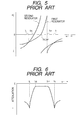
- the parallel resonance frequency f 1p of either resonator, for example, the second resonator 16 is substantially equal to the series resonance frequency f 1s of the first resonator 15, which is the other resonator. Accordingly, reactance curves of these resonators 15, 16 become as shown in Fig. 5.
- a transmission characteristic when a signal is inputted between the first input end 11 and the second input end 13 becomes a characteristic of a band pass filter which has between the series resonance frequency f 2s of the second resonator 16 and the parallel resonance frequency f 1p of the first resonator 16 as the passing band as shown in Fig. 6.
- a lattice filter comprising: two first resonators which are substantially equal to each other in the first series resonance frequency and are substantially equal to each other in the first parallel resonance frequency, that is higher than the first series resonance frequency; two second resonators which are substantially equal to each other in the second series resonance frequency and are substantially equal to each other in the second parallel resonance frequency, that is higher than the second series resonance frequency; two first inductance elements which are substantially equal to each other in the inductance; and two second inductance elements which are substantially equal to each other in the inductance, wherein one of each of the first resonator and the first inductance element is connected to each other in series, and is inserted between the first input end and the first output end while the other of each of the first resonator and the first inductance element is connected to each other in series, and is inserted between the second input end and the second output end; and one of each of the second resonator and the second inductance element is connected to each other
- a reactance curve based on the first resonator and the first inductance element and a reactance curve based on the second resonator and the second inductance element are caused to cross each other in a region of lower frequencies than a series resonance frequency based on the second resonator and the second inductance element.
- the reactance curve based on the first resonator and the first inductance element and the reactance curve basedonthesecondresonatorandthesecondinductanceelement are caused to cross each other in a region of higher frequencies than the parallel resonance frequency of the first resonator.
- first resonators 5, 5 each having the same characteristic respectively.
- second resonators 6, 6 having the same characteristic respectively.
- second inductance elements 8, 8 each having the same inductance in series respectively.
- the inductance of the first inductance element 7 is not always equal to the inductance of the second inductance element 8.
- the first resonator 5 has a series resonance frequency F 1s and a parallel resonance frequency F 1p that is higher than it
- the second resonator 6 has also a series resonance frequency F 2s and a parallel resonance frequency F 2p that is higher than it
- the parallel resonance frequency F 2p of either resonator, for example, the second resonator 6 is lower than the series resonance frequency F 1s of the first resonator 5, which is the other resonator. Accordingly, reactance curves of these two types of resonators 5, 6 become as shown by A, B of Fig. 2 respectively.
- the first resonator 5 and the first inductance element 7 are connected to each other in series, whereby a reactance curve of this series circuit moves to an inductive side (+j side) as indicated by C of Fig. 2, and therefore, its series resonance frequency F 1S ' becomes lower than the series resonance frequency F 1s of the first resonator 5 (the parallel resonance frequency F 1p of the first resonator 5 remains unchanged) .
- the inductance of the first inductance element 7 is set in such a manner that the series resonance frequency F 1S ' at this time substantially coincides with the parallel resonance frequency F 2p of the second resonator 6.
- a transmission characteristic when a signal is inputted between the first input end 1 and the second input end 3 becomes a characteristic of a band pass filter which has between the series resonance frequency f 2s ' based on the second resonator 6 and the second inductance element 8 and the parallel resonance frequency F 1p of the first resonator 6 as the passing band as shown in Fig. 3 so that the passing band becomes wider.
- the series resonance frequency F 1s ' based on the first resonator 5 and the first inductance element 7 substantially coincides with the parallel resonance frequency F 2p of the second resonator 6, ripples within the passing band are reduced.
- a frequency (F L ', F H '), at which a reactance curve based on the first resonator 5 and the first inductance element 7 and a reactance curve based on the second resonator 6 and the second inductance element 8 cross with each other deviates from a frequency (F L , F H ), at which a reactance curve of the first resonator 5 alone and a reactance curve of the second resonator 6 alone cross each other, but the direction of the deviation and the frequency vary with inductance values of the first and second inductance elements 7, 8.
- an angle ⁇ (See Fig. 2) when those reactance curves cross each other is determined by setting of the series resonance frequency (F 1S , F 2S ) and the parallel resonance frequency (F 1P , F 2P ) of each resonator 5, 6 and inductance values of each inductance element 7, 8, but the smaller the angle ⁇ becomes, the wider the band of frequency that attenuates becomes.
- the width of the passing band, the attenuation frequency and the degree of freedom for setting of its band are widened.
- one of each of the first resonator and the first inductance element is connected to each other in series, and is inserted between the first input end and the first output end while the other of each of the first resonator and the first inductance element is connected to each other in series, and is inserted between the second input end and the second output end; and one of each of the second resonator and the second inductance element is connected to each other in series and is inserted between the first input end and the second output end while the other of each of the second resonator and the second inductance element is connected to each other in series and is inserted between the second input end and the first output end, whereby the parallel resonance frequency of the second resonator is caused to substantially coincide with the series resonance frequency based on the first resonator and the first inductance. Therefore, a band pass filter having less ripples and a wide band can be constituted.
- a reactance curve based on the first resonator and the first inductance element and a reactance curve based on the second resonator and the second inductance element are caused to cross each other in a region of lower frequencies than a series resonance frequency based on the second resonator and the second inductance element. Therefore, it is possible to attenuate in a region of lower frequencies than the passing band, and as yet to change the band of the frequency that attenuates by setting inductance values of each inductance element, and the like.
- the reactance curve based on the first resonator and the first inductance element and the reactance curve based on the second resonator and the second inductance element are caused to cross each other in a region of higher frequencies than the parallel resonance frequency of the first resonator. Therefore, it is possible to attenuate in a region of higher frequencies than the passing band, and as yet to change the band of the frequency that attenuates by setting inductance values of each inductance element, and the like.
Landscapes
- Physics & Mathematics (AREA)
- Acoustics & Sound (AREA)
- Filters And Equalizers (AREA)
- Surface Acoustic Wave Elements And Circuit Networks Thereof (AREA)
- Piezo-Electric Or Mechanical Vibrators, Or Delay Or Filter Circuits (AREA)
Abstract
Description
Claims (3)
- A lattice filter, comprising: two first resonators which are substantially equal to each other in a first series resonance frequency and which are substantially equal to each other in a first parallel resonance frequency, that is higher than the first series resonance frequency; two second resonators which are substantially equal to each other in a second series resonance frequency and which are substantially equal to each other in a second parallel resonance frequency, that is higher than the second series resonance frequency; two first inductance elements which are substantially equal to each other in an inductance; and two second inductance elements which are substantially equal to each other in the inductance, whereinone of each of the first resonator and the first inductance element is connected to each other in series, and is inserted between a first input end and a first output end while the other of each of the first resonator and the first inductance element is connected to each other in series, and is inserted between a second input end and a second output end; andone of each of the second resonator and the second inductance element is connected to each other in series and is inserted between the first input end and the second output end while the other of each of the second resonator and the second inductance element is connected to each other in series and is inserted between the second input end and the first output end, whereby the parallel resonance frequency of the second resonator is caused to substantially coincide with a series resonance frequency based on the first resonator and the first inductance.
- The lattice filter according to Claim 1, wherein a reactance curve based on the first resonator and the first inductance element and a reactance curve based on the second resonator and the second inductance element are caused to cross each other in a region of lower frequencies than a series resonance frequency based on the second resonator and the second inductance element.
- The lattice filter according to Claim 1, wherein a reactance curve based on the first resonator and the first inductance element and a reactance curve based on the second resonator and the second inductance element are caused to cross each other in a region of higher frequencies than the parallel resonance frequency of the first resonator.
Applications Claiming Priority (2)
| Application Number | Priority Date | Filing Date | Title |
|---|---|---|---|
| JP2000342370A JP2002152008A (en) | 2000-11-06 | 2000-11-06 | Lattice type filter |
| JP2000342370 | 2000-11-06 |
Publications (2)
| Publication Number | Publication Date |
|---|---|
| EP1204205A2 true EP1204205A2 (en) | 2002-05-08 |
| EP1204205A3 EP1204205A3 (en) | 2004-01-07 |
Family
ID=18816940
Family Applications (1)
| Application Number | Title | Priority Date | Filing Date |
|---|---|---|---|
| EP01309319A Withdrawn EP1204205A3 (en) | 2000-11-06 | 2001-11-02 | Lattice filter with ripple in passing band eliminated and with passing band widened |
Country Status (3)
| Country | Link |
|---|---|
| US (1) | US6624725B2 (en) |
| EP (1) | EP1204205A3 (en) |
| JP (1) | JP2002152008A (en) |
Families Citing this family (4)
| Publication number | Priority date | Publication date | Assignee | Title |
|---|---|---|---|---|
| JP4463262B2 (en) | 2006-11-22 | 2010-05-19 | 富士通メディアデバイス株式会社 | Filter device |
| JP4401380B2 (en) | 2006-11-22 | 2010-01-20 | 富士通メディアデバイス株式会社 | Filter device |
| JP5237138B2 (en) * | 2009-01-27 | 2013-07-17 | 太陽誘電株式会社 | Filters, duplexers, communication modules |
| DE102018107589B4 (en) * | 2018-03-29 | 2020-01-30 | RF360 Europe GmbH | Electroacoustic mesh filter and an RF filter module comprising a mesh filter |
Family Cites Families (6)
| Publication number | Priority date | Publication date | Assignee | Title |
|---|---|---|---|---|
| US2045991A (en) * | 1931-09-19 | 1936-06-30 | Bell Telephone Labor Inc | Wave filter |
| GB434819A (en) * | 1934-03-10 | 1935-09-10 | Western Electric Co | Wave filters |
| US2216937A (en) * | 1938-11-05 | 1940-10-08 | Bell Telephone Labor Inc | Wave filter |
| US5847626A (en) * | 1994-02-22 | 1998-12-08 | Matsushita Electric Industrial Co., Ltd. | Balanced-type surface acoustic wave lattice filter |
| US5933062A (en) | 1997-11-04 | 1999-08-03 | Motorola Inc. | Acoustic wave ladder filter with effectively increased coupling coefficient and method of providing same |
| JP3389911B2 (en) | 2000-02-07 | 2003-03-24 | 株式会社村田製作所 | Surface acoustic wave filter, duplexer and communication device |
-
2000
- 2000-11-06 JP JP2000342370A patent/JP2002152008A/en not_active Withdrawn
-
2001
- 2001-11-02 EP EP01309319A patent/EP1204205A3/en not_active Withdrawn
- 2001-11-02 US US10/003,579 patent/US6624725B2/en not_active Expired - Fee Related
Also Published As
| Publication number | Publication date |
|---|---|
| JP2002152008A (en) | 2002-05-24 |
| US6624725B2 (en) | 2003-09-23 |
| EP1204205A3 (en) | 2004-01-07 |
| US20020053957A1 (en) | 2002-05-09 |
Similar Documents
| Publication | Publication Date | Title |
|---|---|---|
| US6946931B2 (en) | Surface acoustic wave resonator and surface acoustic wave filter | |
| KR102332100B1 (en) | Acoustic wave filter units, multiplexers and composite filter units | |
| US20150222246A1 (en) | Filter device | |
| JP3509773B2 (en) | Surface acoustic wave device, communication device | |
| US11196404B2 (en) | Surface acoustic wave element | |
| JP2005535264A (en) | Filter circuit | |
| US20080100397A1 (en) | Film bulk acoustic resonator filter and duplexer | |
| JP3528049B2 (en) | Surface acoustic wave device, communication device | |
| JPS62261211A (en) | Filter | |
| US6018281A (en) | Resonator type surface acoustic wave ladder filter with voltage variable capacitance element | |
| US4488130A (en) | Microwave integrated circuit, bandpass filter | |
| KR20190122493A (en) | High pass filter | |
| US6624725B2 (en) | Lattice filter with ripple in passing band eliminated and with passing band widened | |
| US6549100B2 (en) | Surface acoustic wave lattice filter with different lattice and series arm capacitance ratios and communication device using same | |
| JPWO2006016544A1 (en) | Duplexer and communication device | |
| US12184267B2 (en) | Surface acoustic wave resonator, acoustic wave filter, and multiplexer | |
| US20050093652A1 (en) | Size scaling of film bulk acoustic resonator (FBAR) filters using impedance transformer (IT) or balun | |
| CA1128135A (en) | Microwave mixing circuit | |
| JP3366477B2 (en) | Vertical composite quad mode SAW filter | |
| KR101035173B1 (en) | A boundary acoustic wave device, and a communicator using the same | |
| JPS62140501A (en) | Mic filter | |
| US6812812B2 (en) | Longitudinally coupled surface acoustic wave resonator filter | |
| GB1109996A (en) | Improvements in or relating to electromechanical band-pass filters | |
| JPS60253302A (en) | Ring-shaped filter | |
| JPS63157501A (en) | Active trap filter |
Legal Events
| Date | Code | Title | Description |
|---|---|---|---|
| PUAI | Public reference made under article 153(3) epc to a published international application that has entered the european phase |
Free format text: ORIGINAL CODE: 0009012 |
|
| AK | Designated contracting states |
Kind code of ref document: A2 Designated state(s): AT BE CH CY DE DK ES FI FR GB GR IE IT LI LU MC NL PT SE TR |
|
| AX | Request for extension of the european patent |
Free format text: AL;LT;LV;MK;RO;SI |
|
| PUAL | Search report despatched |
Free format text: ORIGINAL CODE: 0009013 |
|
| RIC1 | Information provided on ipc code assigned before grant |
Ipc: 7H 03H 9/54 B Ipc: 7H 03H 9/58 A |
|
| AK | Designated contracting states |
Kind code of ref document: A3 Designated state(s): AT BE CH CY DE DK ES FI FR GB GR IE IT LI LU MC NL PT SE TR |
|
| AX | Request for extension of the european patent |
Extension state: AL LT LV MK RO SI |
|
| 17P | Request for examination filed |
Effective date: 20040130 |
|
| AKX | Designation fees paid |
Designated state(s): DE FR GB |
|
| 17Q | First examination report despatched |
Effective date: 20061228 |
|
| STAA | Information on the status of an ep patent application or granted ep patent |
Free format text: STATUS: THE APPLICATION IS DEEMED TO BE WITHDRAWN |
|
| 18D | Application deemed to be withdrawn |
Effective date: 20070508 |