EP1204202A2 - Temperature compensation circuit and a variable gain amplification circuit - Google Patents
Temperature compensation circuit and a variable gain amplification circuit Download PDFInfo
- Publication number
- EP1204202A2 EP1204202A2 EP01309373A EP01309373A EP1204202A2 EP 1204202 A2 EP1204202 A2 EP 1204202A2 EP 01309373 A EP01309373 A EP 01309373A EP 01309373 A EP01309373 A EP 01309373A EP 1204202 A2 EP1204202 A2 EP 1204202A2
- Authority
- EP
- European Patent Office
- Prior art keywords
- signal
- current
- mos transistor
- amplifier
- source
- Prior art date
- Legal status (The legal status is an assumption and is not a legal conclusion. Google has not performed a legal analysis and makes no representation as to the accuracy of the status listed.)
- Granted
Links
- 230000003321 amplification Effects 0.000 title claims description 10
- 238000003199 nucleic acid amplification method Methods 0.000 title claims description 10
- 238000004891 communication Methods 0.000 claims description 5
- 238000000034 method Methods 0.000 claims description 5
- 238000010586 diagram Methods 0.000 description 11
- 230000005540 biological transmission Effects 0.000 description 8
- 238000006243 chemical reaction Methods 0.000 description 5
- 230000010355 oscillation Effects 0.000 description 5
- 101000870046 Sus scrofa Glutamate dehydrogenase 1, mitochondrial Proteins 0.000 description 3
- 101001005165 Bos taurus Lens fiber membrane intrinsic protein Proteins 0.000 description 2
- -1 MN51 Proteins 0.000 description 2
- 101100472152 Trypanosoma brucei brucei (strain 927/4 GUTat10.1) REL1 gene Proteins 0.000 description 2
- 238000012546 transfer Methods 0.000 description 2
- 101710115990 Lens fiber membrane intrinsic protein Proteins 0.000 description 1
- 102100026038 Lens fiber membrane intrinsic protein Human genes 0.000 description 1
- 238000004458 analytical method Methods 0.000 description 1
- 230000003466 anti-cipated effect Effects 0.000 description 1
- 230000009286 beneficial effect Effects 0.000 description 1
- 230000003247 decreasing effect Effects 0.000 description 1
- 238000013461 design Methods 0.000 description 1
- 239000012535 impurity Substances 0.000 description 1
- 238000002955 isolation Methods 0.000 description 1
- 238000004519 manufacturing process Methods 0.000 description 1
- 229910044991 metal oxide Inorganic materials 0.000 description 1
- 150000004706 metal oxides Chemical class 0.000 description 1
- 238000012986 modification Methods 0.000 description 1
- 230000004048 modification Effects 0.000 description 1
- 239000004065 semiconductor Substances 0.000 description 1
Images


Classifications
-
- H—ELECTRICITY
- H03—ELECTRONIC CIRCUITRY
- H03G—CONTROL OF AMPLIFICATION
- H03G1/00—Details of arrangements for controlling amplification
- H03G1/04—Modifications of control circuit to reduce distortion caused by control
Definitions
- the present invention relates to a temperature compensation circuit performing a temperature compensation with respect to a gain characteristic of a variable gain amplifier fabricated by MOS transistors and gain-controlled by an external gain control signal, and a variable gain amplification circuit using the same temperature compensation circuit.
- a variable gain amplifier has been developed so that a gain varies with an exponential function in respect to a gain control signal Vc.
- a U.S. Patent No. 6,215,989 B1 describes a variable gain amplifier fabricated by bipolar transistors having an input/ output characteristic representing an exponential function.
- the applicant provides a technique of realizing a variable gain amplifier utilizing a fact that the MOS transistor operating in a weak inversion region has an exponential-law characteristic expressed by an expression (4) (refer to the U.S. Patent Application No. 09/950,630, the entire contents of which are incorporated herein by reference).
- a temperature compensation circuit performing a temperature compensation with respect to a gain characteristic of a variable gain amplifier fabricated by MOS transistors and gain-controlled by an external gain control signal
- the apparatus comprising: a signal source configured to output a first signal corresponding to a temperature change of an ambient temperature to a predetermined temperature; a multiplier configured to multiply the external gain control signal and the first signal and output a second signal proportional to the temperature change and the first signal; and a temperature compensation device configured to transfer the second signal to the variable gain amplifier to perform the temperature compensation with respect to the variable gain amplifier.
- the present invention realizes a variable gain amplifier circuit using MOS transistors operable in a weak inversion region. It is generally known that an input/output characteristic shifts from a square-law characteristic to an exponential-law characteristic when a density of current flowing through a MOS transistor is decreased. The region where a MOS transistor has the exponential-law characteristics is referred to as a weak inversion region.
- a region having a square-law characteristic is referred to as a strong inversion region, and a gate-to-source voltage when it is changed from the weak inversion region to the strong inversion region is referred to as a threshold voltage.
- VGS gate-to-source voltage
- VTH threshold voltage
- ID - V GS characteristic In weak inversion region, a ID - V GS characteristic (input/output characteristic) is expressed by where ID is a drain current, I ON is an ON current, and V ON is an ON voltage, and I ON , V ON and n are constants determined by a production process of a MOS transistor (for example, doping density of impurities).
- VT (k ⁇ T)/q, where VT: thermal voltage, a k: Boltzmann constant, T: temperature, and q: elementary charge quantity.
- the gain control signal (first gain control signal) Vc can be exponentially gain-controlled when a variable gain amplifier 102 shown in FIGS. 7 and 8 is operated in the weak inversion region.
- a gain characteristic of an output current to an input current is expressed by an expression (2) with respect to the second gain control signal Vy, and the transfer function of gain control signal converter 702 is expressed by an equation (3).
- a concrete circuit configuration of a current source 801 of FIG. 8 refers to FIG. 9, and a gain control signal current 1c flowing through a current source 901 of FIG. 9 indicates the current proportional to a gain control signal Vc.
- b indicates a proportional constant.
- the present invention is directed to temperature compensation of a gain of the variable gain amplifier circuit.
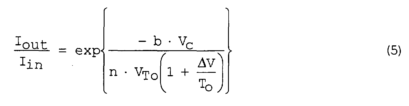
- thermal voltage VT of the equation (4) is represented as a thermal voltage VTo with a predetermined temperature To, and a temperature change of an ambient temperature T to a predetermined temperature To, for example, a difference is indicated by ⁇ T, VT is expressed with VTo (1 + ⁇ T/To), and the equation (4) is converted to an equation (5).
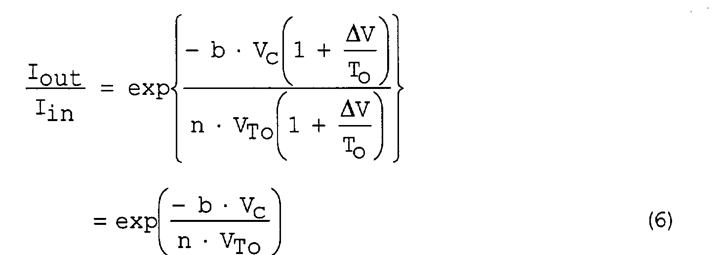
- the equation (6) is the equation having no temperature dependency. It can be understood to convert a gain control signal Vc into a signal represented by Vc (1+ ⁇ T/To) to avoid a temperature dependency of a gain characteristic of an output current I out to an input current I in .
- FIG. 1A shows a block diagram expressing a first basic concept of a variable gain amplification circuit performing a temperature compensation with respect to a gain of a variable gain amplifier according to an embodiment of the present invention.
- the output current 1c( ⁇ T) as the multiplication result is used as a gain control signal of the variable gain amplifier.
- a gain control signal input terminal 103 is a terminal to receive a gain control signal Vc supplied from the outside.
- An amplifier 105 has a function as a voltage - current converter that converts the gain control signal Vc to the gain control signal current 1c in addition to a function as an amplifier.
- FIG. 1B shows a block diagram illustrating a second basic concept of a variable gain amplification circuit performing a temperature compensation with respect to a gain of a variable gain amplifier according to an embodiment of the present invention.
- the signal I CNT1(T) makes it possible to change a proportional coefficient of temperature into a desired value from 1/To.
- the gain control signal I CNTO that does not depend upon a temperature substantially can be generated by a conventional differential amplifier 105b using a source degenerate resistor.
- FIG. 2 is a circuit diagram showing a concrete circuit 101a of the current source 101 having a temperature dependency as shown in FIGS. 1A and 1B.
- a reference “M” shows a MOS (Metal Oxide Semiconductor) transistor, and a subscript “P” indicates a P type and a subscript “N” indicates an N type.
- the circuit of current source 101a is known broadly as a Widlar current source.
- Widlar current source is fabricated by bipolar transistors.
- MOS transistors are used for integrating the current source, and MOS transistors MN 30 and MN31 are operated in weak inversion regions to output a current with a temperature dependency.
- the current source 101a comprises a MOS transistor MN30 having a source terminal connected to a ground terminal and a MOS transistor MN31 having a source terminal connected to the ground terminal via a resistor R T .
- the gate terminal of the MOS transistor MN30 is connected to the gate and drain terminals of the MOS transistor MN31. Substantial equal currents flow through the drain terminals of the MOS transistor MN30 and MN31.
- the MOS transistors MN30 and MN31 are operated in the weak inversion region.
- the transistors MN30 and MN31 operate as a current mirror circuit, and the gate terminal and drain terminal of the transistor MP31 construct the input terminal of the current mirror circuit.
- the drain terminal of the transistor MN30 is connected to the output terminal of the current mirror circuit, the source terminal thereof is grounded, and the gate terminal thereof is connected to the gate and drain terminals of the transistor MN31.
- the source terminal of the transistor MN31 is grounded via a resistor RT.
- the drain terminal of the transistor MN32 is connected to the input terminal of the current mirror circuit, and the source terminal thereof is connected to the drain terminal of the transistor MN31, and the gate terminal thereof is connected to the drain terminal of the transistor MN30 and a start up circuit 200.
- This current source 101a has two stable points of a current value, and the start up circuit 200 is provided for making the current source active to obtain a predetermined current value.
- the W/L ratio (W: gate width, L: gate length) of the transistors MN30 and MN31 is set at 1:M.
- the transistors MN30 and MN31 are designed to increase W for the purpose of reducing a current density so that they operate in the weak inversion region.
- the operation of the current source 101a is explained hereinafter.
- the input/output characteristic of the transistors MN30 and MN31 is expressed with the equation (1) to operate the transistor MN30 and MN31 in the weak inversion region. Therefore, the voltage VR applied to both ends of the resistor RT is expressed with the following equations. Therefore, the operating current I out (T) is expressed with an equation (8).
- Io (n * lnM/RT) VTo. Therefore, it is understood that the current source 101a has a temperature dependency.
- FIG. 3 shows a concrete circuit 101b of the current source 101 of FIGS. 1A and 1B having a temperature dependency.
- the temperature coefficient is set to a value different from 1/To.
- the circuit of FIG. 3 differs from that of FIG. 2 in inputting an output of the transistor MP32 and an output of a constant current source P*Io (P indicates an adjustable coefficient) without a temperature dependency to a current mirror circuit fabricated by transistors MN33 and MN34, and extracting an output current I out (T) from transistor MN34 of the current mirror circuit.
- P*Io P indicates an adjustable coefficient
- the output current Iout (T) is expressed with the following equations.
- the temperature coefficient can be changed by selecting P properly.
- FIG. 4 shows a circuit of a current source having substantially no temperature dependency, and this current source is used as a current source 501 of FIG. 5 having no temperature dependency as described below.
- This circuit uses that the polarity of a temperature dependency of thermal voltage V T and that of a temperature dependency of the threshold voltage V TH of a MOS transistor is different. In other word, results obtained by multiplying desired coefficients ( ⁇ , ⁇ ) by respective current outputs are added by an adder 403. The addition result is output as the current having substantially no temperature dependency to an output terminal 404.
- a circuit 401 corresponds to the current source 101a of FIG. 2.
- the current source is proportional to the thermal voltage V T and has a temperature dependency.
- a circuit 402 comprises a current source proportional to the threshold voltage V TH and having a temperature dependency.
- the current source comprises a MOS transistor M N40 whose source terminal is grounded, a resistor R TH through which a gate terminal of the MOS transistor M N40 is grounded, and a MOS transistor M N41 having a gate terminal connected to a drain terminal of the MOS transistor M N40 and a source grounded via the resistor R TH .
- the drain terminal of the MOS transistor M N41 is connected to an output terminal.
- V GS When the transistor MN40 is operated in the weak inversion region, V GS can be approximated to the threshold voltage Therefore, an output current of the circuit 402 is expressed by an equation (11).
- V THo expresses a threshold voltage of predetermined temperature
- q expresses a temperature coefficient of a threshold voltage
- R TH expresses a resistor.
- the circuit 402 comprises a current source having a threshold voltage as a reference, and is referred to as a threshold reference circuit.
- the current flowing through the transistor MN40 is based on a current depended upon the thermal voltage V T .
- V GS can be approximated to the threshold voltage if the transistor MN40 is not operated in the weak inversion region as described above. Therefore, no problem occurs even if a bias is set using the current depended upon V T . Even if the transistor MN40 is used in the weak inversion region, the temperature dependency of the threshold voltage can be anticipated. Therefore, there is a case that the transistor MN40 need not be used always in the weak inversion region.
- FIG. 5 shows a multiplier 104 to generate a current having a temperature dependency and a gain control current 1c.
- the multiplier 104 comprises current sources 501, 502 and 503 and MOS transistors M P50 , M p51 , M P52 and M P53 .
- the current source 501 is connected to a node of drain terminals of the MOS transistors M P50 and M p51 and the current source 502 is connected to a node of drain terminals of the MOS transistors M P52 and M p53 .
- the gate of the MOS transistors M p51 and M P52 is connected to a voltage source V BB .
- the gate and source terminals of the MOS transistor M P50 and the gate terminal of the MOS transistor M P53 is grounded via the current source 503.
- the source terminals of the MOS transistors M P51 and M p52 are grounded.
- the source terminal of the MOS transistor M p53 is connected to the output terminal 504.
- the multiplier 104 makes a gate-to-gate voltage common to two differential transistor pairs M P50 , M p51 and M P52 , M P53 . Therefore, the ratio between the tail current Io and gain control current Ic can be substantially equalized to the ratio between the tail current Io (1+ ⁇ T/To) and output current Ic (T).
- the tail current Io is output by a current source 501 and a current having substantially no temperature dependency
- the gain control current Ic is a gain control current before the temperature compensation that is output by a current source 503.
- the tail current Io (1+ ⁇ T/To) is a current with a temperature dependency output from the current source 502, and the output current Ic (T) is a current obtained at an output terminal 504.
- the output current 1c (T) is determined by multiplication of a temperature variable (1+ ⁇ T/To) of the tail current 1o (1+ ⁇ T/To) having the temperature dependency with the gain control current 1c before temperature compensation. Then it is expressed this with the following equations.
- This equation is an equation when transistors MP50, MN51, MP52 and MP53 are operated in the weak inversion region, that is, when the transistors MP50, MN51, MP52 and MP53 had an exponential input/output characteristic.
- this equation can be applied in approximation even where the transistor MP50, MN51, MN52 and MP53 had a square-law input/output characteristic.
- the current source with the temperature coefficient of 1/To is applied, but it can be substituted for a current source with temperature coefficient different from 1/To as shown in FIG. 3.
- the above embodiment is described for the temperature compensation of FIG. 1A, but is applicable to the temperature compensation of FIG. 1B.
- the multiplication of the gain control current signal Vc with the current of the current source 101 having a temperature dependency can be performed by a multiplier 104 shown in FIG. 5.
- a current source having a temperature dependency uses the current source of FIG. 2 or the current source of FIG. 3.
- the control current subjected to a temperature compensation is I CNT1(T) of FIG. 1B.
- the circuit for gain control current having substantially no temperature dependency may use a conventional differential amplifier 105b. Therefore, detailed description of the circuit is omitted.
- the gain control current Ic (T) having a temperature dependency is generated according to the equation (12), and is input to the current source 901 shown in FIG. 9.
- the gain control current Ic(T) having a temperature dependency is generated by adding the current I CNTO having substantially no temperature dependency to the current I CNT1 (T) having a temperature dependency, and then input to a current source 901 shown in FIG. 9.
- a gain equation used for a variable gain circuit using FET that an applicant provides in prior application specification (refer to the U.S. Patent Application No. 09/696,972, the entire contents of which are incorporated herein by reference) is expressed with the following equation (14).
- G MOS exp(-d ⁇ V C ) where d expresses a constant.
- the equation (14) is not a function of VT because it is supposed that the current ID1 of a circuit as shown in FIG. 8 is Io * exp (-d * Vc) in the U.S. Patent Application No. 09/696,972.
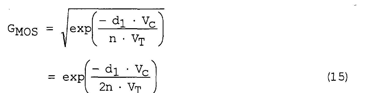
- the gain is expressed with the following equation (15) and is a function of V T . where d1 expresses a constant. Therefore, the present invention can be applied to a variable gain amplifier of the variable gain circuit having FET which is disclosed in the Japanese Patent Application No. 11-306798.
- the temperature compensation can be performed by multiplying an exponent of an equation (15) by a variable k (T) depending upon a temperature.
- FIG. 7 shows a variable gain amplifier 102 utilizing a weak inversion region of a MOS transistor.
- a gain control signal (first gain control signal) Vc for controlling a gain of the variable gain amplifier 102 from the outside is input to the gain control signal input terminal 701.
- the first gain control signal Vc is converted to a second gain control signal Vy by a control signal converter 702, and then is supplied to a variable gain amplifier fabricated by first differential transistor pair (M1, M2).
- the variable gain amplifier is a circuit whose gain is controlled by the second gain control signal Vy, and comprises a first differential transistor pair of N type MOS transistors M1 and M2 which are operated in the weak inversion region.
- a common source terminal of the transistors M1, M2 is connected to a current source 703.
- An input signal current I in to be amplified is supplied from the current source 703 to the differential transistor pair and an output terminal I out is taken out from the drain terminal of the transistor M1.
- the current I in -I out flowing through the drain terminal of the transistor M2 is an unnecessary current, and flows to a power supply and so on.
- the second gain control signal Vy output by control signal conversion 702 is a voltage signal, and input between the gate terminals of the transistor M1 and M2 constructing a differential transistor pair.
- FIG. 8 shows a concrete circuit of gain control signal converter 702 of FIG. 7.
- This gain control signal converter 702 has a second differential transistor pair of N type MOS transistors MN10 and MN11 that operate in the weak inversion region, and a current source 802 is connected to a common terminal of the transistors MN10 and MN11.
- a direct current Io is input to the second differential transistor pair by the current source 802.
- the gate terminal of the transistor MN11 is applied with a constant direct current level by a power supply V BB and the drain terminal of the transistor MN11 is connected to a power supply V DD (not shown), for example.
- the current source 801 for generating a current ID1 to be supplied to the gain control signal converter 702 of FIG. 8 is described in conjunction with FIG. 9.
- N type MOS transistors MN20 and MN21 operate in the weak inversion region similarly to the transistors MN10 and MN11.
- the current Io of the current source 802 of FIG. 8 is generated by the voltage source V BB and transistor MN21 of FIG. 9.
- Ic expresses a current proportional to the voltage of the second gain control signal Vc (a proportion coefficient is u). Since the current IC is generated in easy using a voltage-to-current converter such as a differential circuit wherein a source degenerate resistor is connected between source terminals, the detail description is omitted.
- the source of the transistor MN20 is grounded, and its drain terminal is connected to an input terminal of a current mirror circuit fabricated by transistors MN20 and MP21 (gate and drain terminals of the transistor MP20).
- the drain terminal of the transistor MP21 which is an output terminal of the current mirror circuit is connected to the drain and gate terminals of the transistor MN10.
- the current 1D1 Io * exp(-b * Vc/VT) of the current source 801 of FIG. 8 is generated by a part of a circuit of FIG. 9.
- the ratio of an input current to an output current represents an exponential-law characteristic as is indicated in the equation (4).
- a variable gain amplification circuit related to an embodiment of the present invention is suitable for a radio communication apparatus of portable communication equipment using a direct conversion system.
- FIG. 6 shows a configuration of a transceiver of a radio communication apparatus of the direct conversion system.
- the present embodiment is described based on a TDD (Time Division Duplex) system for performing a change of transmission and reception by time sharing, but the present embodiment is not limited to this system.
- TDD Time Division Duplex
- the first and the second transmission baseband signals Ich (TX) and Qch (TX) orthogonal to each other are band-limited by a suitable filter in a baseband signal generator (TX-BB) 601.
- TX-BB baseband signal generator
- These orthogonal baseband signals Ich (TX) and Qch (TX) are amplified, respectively, by baseband signal amplifiers 602 and 603 each comprising a variable gain amplifier related to the present embodiment.
- the orthogonal transmission baseband signals Ich (TX) and Qch (TX) are input to an orthogonal modulator 607 comprising multipliers 604 and 605 and an adder 606.
- the orthogonal modulator 607 modulates, with the baseband signals Ich (TX) and Qch (TX), two orthogonal local oscillation signals generated by dividing a local oscillation signal (frequency fLO11) of a local oscillator 608 by a 90° phase shifter (90° -PS) 609.
- An unnecessary component is removed from a modulated signal output from the orthogonal modulator 607 (a RF (radio) signal) by a band passage filter 610 and input to an power amplifier (PA) 611.
- PA power amplifier
- the RF signal is adjusted to a suitable signal level by a RF stage variable gain amplifier provided on an input stage based on a control signal from a controller 624 and then is amplified to a predetermined power level.
- the controller 624 is so constructed as to generate a control signal corresponding to a predetermined transmission power and a received signal power.
- the controller 624 comprises a table which outputs control data corresponding to the predetermined transmission power and receiver signal power and a D/A converter which convert the control data to an analog control signal.
- the control signal from the controller 624 is supplied to the variable gain amplifiers 602,603,611,615,621 and 622 to control the gains of the variable gain amplifiers.
- An amplified RF signal is emitted as a radio wave from an antenna (ANT) 613 via a transmit-receive switch (T/R) 612 or duplexer.
- ANT antenna
- T/R transmit-receive switch
- a.received RF signal from the antenna 613 is input to a low-noise amplifier (LNA) 614 via the transmit-receive switch 612.
- LNA low-noise amplifier
- the received RF signal amplified by low-noise amplifier 614 is input to an orthogonal demodulator (down converter) 618 comprising a divider and two multipliers 616 and 617 via a filter 615.
- the orthogonal demodulator 618 frequency-converts the received RF signal by multiplying the received RF signal and two orthogonal local oscillation signals, and outputs the orthogonal first and the second baseband signals Ich (RX) and Qch (RX).
- the two orthogonal local oscillation signals are generated by dividing a local oscillation signal (frequency fL010) of a local oscillator 619 by a 90° phase shifter (90° -PS) 620.
- These baseband signals Ich (RX) and Qch (RX) are amplified by baseband amplifiers 621 and 622 each comprising the variable gain amplification circuit related to the embodiment of the present invention.
- the amplified baseband signals Ich (RX) and Qch (RX) are input to a baseband signal processor (RX-BB) 623 and demodulated by it to be reproduced in an original data signal.
- RX-BB baseband signal processor
- the gain on the receiver is controlled by the low-noise amplifier 614 and the baseband amplifiers 621 and 622.
- a variable gain range of a RF stage variable gain amplifier arranged in an input stage of the power amplifier 611 for example is limited by an input-to-output isolation. For this reason, it is required to provide the baseband signal amplifiers 621 and 622 with a variable gain amplification function for a transmission power control.
- the baseband signal amplifiers 602, 603, 621 and 622 treat a baseband signal of a relatively narrow band, these amplifiers may be fabricated by MOS transistors inferior to the bipolar transistor in a frequency characteristic. Therefore, a variable gain amplification circuit realized by MOS transistors as being the embodiments of the present invention is suitable for radio equipment providing the baseband signal amplifiers 602, 603, 621 and 622 with a variable gain control function.
- a temperature change of a gain characteristic of a variable gain amplifier using a MOS transistor can be suppressed.
Landscapes
- Amplifiers (AREA)
- Control Of Amplification And Gain Control (AREA)
Abstract
Description









Claims (17)
- A temperature compensation circuit characterized by performing a temperature compensation with respect to a gain characteristic of a variable gain amplifier(102) fabricated by MOS transistors and gain-controlled by an external gain control signal(Vc), the circuit characterized by comprising:signal source means (101) for outputting a first signal (Ic) corresponding to a temperature change of an ambient temperature to a predetermined temperature; andmultiplier means (104) for multiplying the external gain control signal (Vc) and the first signal (Ic) and output a second signal (Ic(T)) proportional to the temperature change and the first signal to the variable gain amplifier to perform the temperature compensation with respect to the variable gain amplifier.
- A temperature compensation circuit according to claim 1, characterized by further comprising differential amplifier means (105b) for converting the external gain control signal (Vc) into a third signal (ICNT0) having substantially no temperature dependency, and adder means (106) for adding the second signal (ICNT1 (T)) and the third signal (ICNT0) to output a fourth signal (Ic(T)) to the variable gain amplifier (102).
- A circuit according to claim 1 or 2, characterized by including a current mirror circuit arranged between the signal source means (101) and the multiplier means (104), the current mirror circuit comprising MOS transistors (MN33, MN34) and a constant current source (P · Io) having substantially no temperature dependency.
- A circuit according to any one of claims 1 to 3, characterized by including means (105, 105b) for amplifying the external gain control signal and converting it into a gain control current to be supplied to the multiplier means (104) as the second signal.
- A circuit according to any one of claims 1 to 4, characterized by including a start-up circuit for driving the signal source.
- A circuit according to any one of claims 1 to 5, characterized in that the signal source (101a) comprises a first MOS transistor (MN30) whose source terminal is grounded, a second MOS transistor (MN31) having gate and drain terminals connected to a gate of the first MOS transistor, and a resistor (RT) through which a source terminal of the second MOS transistor (MN31) is grounded, and substantially identical currents flow through the drain terminals of the first and second MOS transistors, and the first and second MOS transistors operates in a weak inversion region.
- A circuit according to claim 6, characterized in that the signal source means (101a) includes a third MOS transistor (MN32) connected to the gate and drain terminals of the second MOS transistor and a start-up circuit (200) connected to a gate of the third MOS transistor to drive the signal source.
- A circuit according to any one of claims 1 to 7, characterized in that the multiplier means (104) includes a constant current source (501) having substantially no temperature dependency, the multiplier equalizing substantially a ratio between an output (Io) of the constant current source and the external gain control signal and a ratio between the first signal and the second signal.
- A circuit according to claim 8, characterized in that the constant current source (501) includes a first current source (401) that outputs a current proportional to the thermal voltage (Vt), a second current source (402) that outputs a current proportional to a threshold voltage of the MOS transistors, and an adder (403) configured to add the current of the first current source and the current of the second current source to generate a current having substantially no thermal dependency.
- A circuit according to claim 9, characterized in that the first current source (401) comprises a first MOS transistor (MN30) whose source terminal is grounded, a second MOS transistor (MN31) having gate and drain terminals connected to a gate of the first MOS transistor, and a resistor (RT) through which a source terminal of the second MOS transistor (MN31) is grounded, and substantially identical currents flow through the drain terminals of the first and second MOS transistors, and the first and second MOS transistors operates in a weak inversion region.
- A circuit according to claim 10, characterized in that the second current source (402) comprises a third MOS transistor (MN40) whose source terminal is grounded, a resistor (RTH) through which a gate of the third MOS transistor is grounded, and a fourth MOS transistor having a gate connected to a drain of the third MOS transistor and a source grounded via the resistor (RTH).
- A circuit according to claim 11, characterized in that the third MOS transistor (MN40) is operated in a weak inversion region.
- A circuit according to claims 1 or 2, characterized in that the multiplier means (104) comprises a first current source (501) generating a tail current Io having substantially no temperature dependency, a second current source (502) generating a tail current Io (1+ΔT/To) having a temperature dependency, a third current source (503) generating a gain control current Ic before the temperature compensation, and differential MOS transistor pairs (MP50, Mp51 and MP52, MP53) connected to the first and second current sources, respectively, and outputs a current represented by Ic(1 + ΔT/To) as the second signal.
- A circuit according to claim 13, characterized in that the differential MOS transistor pairs (MP50, Mp51 and MP52, MP53) are operated in the weak inversion region.
- A variable gain amplification circuit,
characterized by comprising:a variable gain amplifier fabricated by MOS transistors and gain-controlled by an external gain control signal; andthe temperature compensation circuit according to any one of claims 1 to 14. - A radio communication apparatus comprising:a transmitter including a baseband signal generator to generate a baseband signal, a baseband signal amplifier to amplify the baseband signal, an orthogonal modulator to orthogonal-modulate the baseband signal amplified by the amplifier, and a power amplifier to amplify a modulated signal of the orthogonal modulator; anda receiver including a low-noise amplifier to amplify a received signal, an orthogonal demodulator to orthogonal-demodulate the received signal amplified by the amplifier, a baseband signal amplifier to amplify a demodulated signal of the orthogonal demodulator, and a baseband signal processor to process the baseband signal obtained by the baseband signal amplifier of the receiver,each of the baseband signal amplifiers and power amplifier of the transmitter being configured by the variable gain amplifier circuit according to any one of claims 1 to 15, and each of the baseband amplifiers and low-noise amplifier of the receiver being configured by the variable gain amplifier circuit according to claim 1 to 15.
- A temperature compensation method characterized by performing a temperature compensation with respect to a gain characteristic of a variable gain amplifier fabricated by MOS transistors and gain-controlled by an external gain control signal, the method comprising:generating a first signal (Ic) corresponding to a temperature change of an ambient temperature to a predetermined temperature; andmultiplying the external gain control signal (Vc) and the first signal (Ic) and output a second signal (Ic(T)) proportional to the temperature change and the first signal to the variable gain amplifier to perform the temperature compensation with respect to the variable gain amplifier.
Applications Claiming Priority (2)
| Application Number | Priority Date | Filing Date | Title |
|---|---|---|---|
| JP2000337175 | 2000-11-06 | ||
| JP2000337175A JP3852906B2 (en) | 2000-11-06 | 2000-11-06 | Temperature compensation circuit and variable gain amplifier circuit |
Publications (3)
| Publication Number | Publication Date |
|---|---|
| EP1204202A2 true EP1204202A2 (en) | 2002-05-08 |
| EP1204202A3 EP1204202A3 (en) | 2003-06-18 |
| EP1204202B1 EP1204202B1 (en) | 2006-08-09 |
Family
ID=18812601
Family Applications (1)
| Application Number | Title | Priority Date | Filing Date |
|---|---|---|---|
| EP01309373A Expired - Lifetime EP1204202B1 (en) | 2000-11-06 | 2001-11-06 | A Radio Communication Apparatus |
Country Status (4)
| Country | Link |
|---|---|
| US (2) | US6844782B2 (en) |
| EP (1) | EP1204202B1 (en) |
| JP (1) | JP3852906B2 (en) |
| DE (1) | DE60122089T2 (en) |
Cited By (2)
| Publication number | Priority date | Publication date | Assignee | Title |
|---|---|---|---|---|
| WO2004107566A3 (en) * | 2003-05-23 | 2005-06-02 | Qualcomm Inc | Temperature and process compensation of mosfet operating in sub-threshold mode |
| EP2469706A3 (en) * | 2006-04-24 | 2012-08-08 | Icera Canada ULC | Low noise CMOS transmitter circuit with high range of gain |
Families Citing this family (19)
| Publication number | Priority date | Publication date | Assignee | Title |
|---|---|---|---|---|
| JP3585822B2 (en) | 2000-09-28 | 2004-11-04 | 株式会社東芝 | Wireless communication device using variable gain amplifier |
| JP3852906B2 (en) * | 2000-11-06 | 2006-12-06 | 株式会社東芝 | Temperature compensation circuit and variable gain amplifier circuit |
| US7167045B1 (en) * | 2004-06-07 | 2007-01-23 | Marvell International Ltd. | System and method for modifying output power of an information communication system |
| US7451174B2 (en) * | 2005-03-16 | 2008-11-11 | Anadec Gmbh | Multi-level soft detector-quantizer |
| US7259620B2 (en) * | 2005-06-27 | 2007-08-21 | Linear Technology Corporation | Wide dynamic range switching variable gain amplifier and control |
| US7262661B2 (en) * | 2005-06-27 | 2007-08-28 | Linear Technology Corporation | Variable gain amplifier with temperature compensation and gain linearity enhancement |
| US20070105516A1 (en) * | 2005-11-10 | 2007-05-10 | Hickman Barton T | Automatic compensation of gain versus temperature |
| JP2007228399A (en) * | 2006-02-24 | 2007-09-06 | Toshiba Corp | Voltage controlled current source and variable gain amplifier |
| KR100657770B1 (en) * | 2006-02-28 | 2006-12-14 | 포스데이타 주식회사 | Local signal generator and method for generating local signal for wireless communication and base station of wireless communication system using same |
| JP5019850B2 (en) * | 2006-11-07 | 2012-09-05 | 日本信号株式会社 | Gain control device for current mirror circuit |
| TWI339007B (en) * | 2006-11-21 | 2011-03-11 | Ind Tech Res Inst | Design method of low frequency analog circuit and low frequency analog circuit using the same |
| JP5312982B2 (en) * | 2009-02-26 | 2013-10-09 | ルネサスエレクトロニクス株式会社 | RF power amplifier circuit and RF power module using the same |
| US8669808B2 (en) * | 2009-09-14 | 2014-03-11 | Mediatek Inc. | Bias circuit and phase-locked loop circuit using the same |
| US8629673B1 (en) * | 2010-12-22 | 2014-01-14 | Rockwell Collins, Inc. | Power detection for high power amplifier applications |
| JP5590154B2 (en) * | 2011-01-17 | 2014-09-17 | 日本電気株式会社 | Digital demodulation circuit using automatic gain control circuit with temperature compensation function |
| US10613560B2 (en) * | 2016-08-05 | 2020-04-07 | Mediatek Inc. | Buffer stage and control circuit |
| JP2021083054A (en) * | 2019-11-22 | 2021-05-27 | エイブリック株式会社 | Oscillation circuit |
| CN116094476B (en) * | 2023-04-11 | 2024-07-02 | 上海安其威微电子科技有限公司 | Circuit structure with gain compensation |
| CN118100816B (en) * | 2024-04-22 | 2024-07-12 | 基合半导体(宁波)有限公司 | Operational amplifier structure and integrated circuit |
Family Cites Families (5)
| Publication number | Priority date | Publication date | Assignee | Title |
|---|---|---|---|---|
| FR2729762A1 (en) * | 1995-01-23 | 1996-07-26 | Sgs Thomson Microelectronics | COMPENSATED VOLTAGE DETECTION CIRCUIT IN TECHNOLOGY AND TEMPERATURE |
| US6028478A (en) * | 1998-07-13 | 2000-02-22 | Philips Electronics North America Corporation | Converter circuit and variable gain amplifier with temperature compensation |
| JP3469486B2 (en) | 1998-12-25 | 2003-11-25 | 株式会社東芝 | Variable gain circuit |
| US6766148B1 (en) * | 2000-03-21 | 2004-07-20 | Koninklijke Phillips Electronics N.V. | Switched sideband frequency low-IF transmitter |
| JP3852906B2 (en) * | 2000-11-06 | 2006-12-06 | 株式会社東芝 | Temperature compensation circuit and variable gain amplifier circuit |
-
2000
- 2000-11-06 JP JP2000337175A patent/JP3852906B2/en not_active Expired - Fee Related
-
2001
- 2001-11-05 US US09/985,595 patent/US6844782B2/en not_active Expired - Fee Related
- 2001-11-06 DE DE60122089T patent/DE60122089T2/en not_active Expired - Lifetime
- 2001-11-06 EP EP01309373A patent/EP1204202B1/en not_active Expired - Lifetime
-
2003
- 2003-04-29 US US10/424,745 patent/US20030207671A1/en not_active Abandoned
Cited By (2)
| Publication number | Priority date | Publication date | Assignee | Title |
|---|---|---|---|---|
| WO2004107566A3 (en) * | 2003-05-23 | 2005-06-02 | Qualcomm Inc | Temperature and process compensation of mosfet operating in sub-threshold mode |
| EP2469706A3 (en) * | 2006-04-24 | 2012-08-08 | Icera Canada ULC | Low noise CMOS transmitter circuit with high range of gain |
Also Published As
| Publication number | Publication date |
|---|---|
| JP2002141753A (en) | 2002-05-17 |
| JP3852906B2 (en) | 2006-12-06 |
| DE60122089T2 (en) | 2006-12-14 |
| EP1204202A3 (en) | 2003-06-18 |
| EP1204202B1 (en) | 2006-08-09 |
| DE60122089D1 (en) | 2006-09-21 |
| US6844782B2 (en) | 2005-01-18 |
| US20020084850A1 (en) | 2002-07-04 |
| US20030207671A1 (en) | 2003-11-06 |
Similar Documents
| Publication | Publication Date | Title |
|---|---|---|
| EP1204202B1 (en) | A Radio Communication Apparatus | |
| US7031684B2 (en) | Variable gain amplifier device | |
| US8078122B2 (en) | Interface between digital and analog circuits | |
| US6215989B1 (en) | Variable gain circuit | |
| US11784409B2 (en) | High-resolution phase shifter | |
| US20050099232A1 (en) | Translinear variable gain amplifier | |
| JP2001196880A (en) | Variable gain circuit | |
| US6819183B1 (en) | Temperature and process compensation of MOSFET operating in sub-threshold mode | |
| US6885239B2 (en) | Mobility proportion current generator, and bias generator and amplifier using the same | |
| US7015758B2 (en) | Gain control circuit, and a radio communication apparatus using the same | |
| JP3798724B2 (en) | Variable gain amplifier | |
| US6879204B1 (en) | Exponential conversion circuit | |
| US20010013811A1 (en) | Grounded emitter amplifier and a radio communication device using the same | |
| JP3884365B2 (en) | Mobility proportional current generator and bias generator and amplifier using the same | |
| US20050046479A1 (en) | Linear-in-decibel variable gain amplifier | |
| US20050073362A1 (en) | Linear decibel-scale variable gain amplifier | |
| JPH11154877A (en) | Method and apparatus for controlling envelope of radio signal | |
| JP2004128739A (en) | Variable gain circuit and wireless communication apparatus employing the same | |
| JPH1168485A (en) | Frequency conversion device and communication device | |
| US7595626B1 (en) | System for matched and isolated references | |
| WO2012111457A1 (en) | Amplification circuit, and receiving device and communication device using same |
Legal Events
| Date | Code | Title | Description |
|---|---|---|---|
| PUAI | Public reference made under article 153(3) epc to a published international application that has entered the european phase |
Free format text: ORIGINAL CODE: 0009012 |
|
| 17P | Request for examination filed |
Effective date: 20011112 |
|
| AK | Designated contracting states |
Kind code of ref document: A2 Designated state(s): AT BE CH CY DE DK ES FI FR GB GR IE IT LI LU MC NL PT SE TR |
|
| AX | Request for extension of the european patent |
Free format text: AL;LT;LV;MK;RO;SI |
|
| PUAL | Search report despatched |
Free format text: ORIGINAL CODE: 0009013 |
|
| AK | Designated contracting states |
Designated state(s): AT BE CH CY DE DK ES FI FR GB GR IE IT LI LU MC NL PT SE TR |
|
| AX | Request for extension of the european patent |
Extension state: AL LT LV MK RO SI |
|
| AKX | Designation fees paid |
Designated state(s): DE FR GB |
|
| 17Q | First examination report despatched |
Effective date: 20050204 |
|
| GRAP | Despatch of communication of intention to grant a patent |
Free format text: ORIGINAL CODE: EPIDOSNIGR1 |
|
| RTI1 | Title (correction) |
Free format text: A RADIO COMMUNICATION APPARATUS |
|
| GRAS | Grant fee paid |
Free format text: ORIGINAL CODE: EPIDOSNIGR3 |
|
| GRAA | (expected) grant |
Free format text: ORIGINAL CODE: 0009210 |
|
| AK | Designated contracting states |
Kind code of ref document: B1 Designated state(s): DE FR GB |
|
| REG | Reference to a national code |
Ref country code: GB Ref legal event code: FG4D |
|
| REF | Corresponds to: |
Ref document number: 60122089 Country of ref document: DE Date of ref document: 20060921 Kind code of ref document: P |
|
| ET | Fr: translation filed | ||
| PLBE | No opposition filed within time limit |
Free format text: ORIGINAL CODE: 0009261 |
|
| STAA | Information on the status of an ep patent application or granted ep patent |
Free format text: STATUS: NO OPPOSITION FILED WITHIN TIME LIMIT |
|
| 26N | No opposition filed |
Effective date: 20070510 |
|
| PGFP | Annual fee paid to national office [announced via postgrant information from national office to epo] |
Ref country code: FR Payment date: 20121130 Year of fee payment: 12 Ref country code: DE Payment date: 20121031 Year of fee payment: 12 |
|
| PGFP | Annual fee paid to national office [announced via postgrant information from national office to epo] |
Ref country code: GB Payment date: 20121031 Year of fee payment: 12 |
|
| GBPC | Gb: european patent ceased through non-payment of renewal fee |
Effective date: 20131106 |
|
| REG | Reference to a national code |
Ref country code: FR Ref legal event code: ST Effective date: 20140731 |
|
| PG25 | Lapsed in a contracting state [announced via postgrant information from national office to epo] |
Ref country code: DE Free format text: LAPSE BECAUSE OF NON-PAYMENT OF DUE FEES Effective date: 20140603 |
|
| REG | Reference to a national code |
Ref country code: DE Ref legal event code: R119 Ref document number: 60122089 Country of ref document: DE Effective date: 20140603 |
|
| PG25 | Lapsed in a contracting state [announced via postgrant information from national office to epo] |
Ref country code: GB Free format text: LAPSE BECAUSE OF NON-PAYMENT OF DUE FEES Effective date: 20131106 Ref country code: FR Free format text: LAPSE BECAUSE OF NON-PAYMENT OF DUE FEES Effective date: 20131202 |