EP1204201A2 - Apparatus and method for producing an RF transmision signal - Google Patents
Apparatus and method for producing an RF transmision signal Download PDFInfo
- Publication number
- EP1204201A2 EP1204201A2 EP01000592A EP01000592A EP1204201A2 EP 1204201 A2 EP1204201 A2 EP 1204201A2 EP 01000592 A EP01000592 A EP 01000592A EP 01000592 A EP01000592 A EP 01000592A EP 1204201 A2 EP1204201 A2 EP 1204201A2
- Authority
- EP
- European Patent Office
- Prior art keywords
- signal
- frequency
- combining
- producing
- synthesizer
- Prior art date
- Legal status (The legal status is an assumption and is not a legal conclusion. Google has not performed a legal analysis and makes no representation as to the accuracy of the status listed.)
- Granted
Links
Images

Classifications
-
- H—ELECTRICITY
- H03—ELECTRONIC CIRCUITRY
- H03L—AUTOMATIC CONTROL, STARTING, SYNCHRONISATION OR STABILISATION OF GENERATORS OF ELECTRONIC OSCILLATIONS OR PULSES
- H03L7/00—Automatic control of frequency or phase; Synchronisation
- H03L7/06—Automatic control of frequency or phase; Synchronisation using a reference signal applied to a frequency- or phase-locked loop
- H03L7/16—Indirect frequency synthesis, i.e. generating a desired one of a number of predetermined frequencies using a frequency- or phase-locked loop
- H03L7/22—Indirect frequency synthesis, i.e. generating a desired one of a number of predetermined frequencies using a frequency- or phase-locked loop using more than one loop
- H03L7/23—Indirect frequency synthesis, i.e. generating a desired one of a number of predetermined frequencies using a frequency- or phase-locked loop using more than one loop with pulse counters or frequency dividers
-
- H—ELECTRICITY
- H03—ELECTRONIC CIRCUITRY
- H03C—MODULATION
- H03C3/00—Angle modulation
- H03C3/38—Angle modulation by converting amplitude modulation to angle modulation
- H03C3/40—Angle modulation by converting amplitude modulation to angle modulation using two signal paths the outputs of which have a predetermined phase difference and at least one output being amplitude-modulated
Definitions
- the invention relates generally to radio frequency communications and, more particularly, to frequency channel spacing in radio frequency communications.
- n is a small integer number.
- the channel spacing can be, for example, 4.6 MHz, 4.8 MHz, 5.0 MHz, 5.2 MHz, etc.
- Examples of RF systems that use such channel spacing include WCDMA systems and UMTS systems.
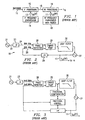
- FIGURE 1 diagrammatically illustrates a conventional example of an architecture for producing an output transmit frequency f TX having a desired channel spacing dependent upon the desired raster, for example, the channel spacing defined in the foregoing equation.
- a baseband signal 11 is input to an intermediate frequency (IF) processing section 12 where it is combined with a signal 13 produced by a frequency synthesizer 14.
- the signal 13 has a frequency f LO (IF) that, when combined with the baseband signal 11 produces an IF signal 15.
- the frequency of the signal 13 is a fixed frequency.
- the IF signal 15 is input to an RF processing section 16, where it is combined with a signal 17 produced by a frequency synthesizer 18.
- the RF processing section 16 produces at 19 an output frequency f TX having the desired channel spacing.
- the signal 17 output from the frequency synthesizer 18 has a frequency designated in FIGURE 1 as f LO (RF).
- the frequency synthesizer 18 has raster capability which provides the desired channel spacing in the output frequency f TX .
- FIGURE 2 diagrammatically illustrates one example of the conventional frequency synthesizer 18 of FIGURE 1, namely an integer phase locked loop (PLL) example.
- a comparison frequency generator includes an oscillator 21 and a divider 23.
- the oscillator 21 provides a frequency reference 22 which is applied to a divider 23 that divides the frequency reference by a divisor R to produce at 24 a comparison frequency of 200 KHz.
- This 200 KHz comparison frequency corresponds to a desired 200 KHz raster.
- a divider 25 divides the output signal 17 by a divisor N in order to obtain at 26 another 200 KHz signal.
- the remaining components of FIGURE 2, namely the frequency generator 27, the phase detector 28, the charge pump 29 and the loop filter 30 are well known in the PLL art, both structurally and functionally, and will therefore not be described in further detail.
- the comparison frequency at 24 in order to achieve the desired 200 KHz raster, the comparison frequency at 24 must be set to 200 KHz, which also requires the divider 25 to produce a 200 KHz signal at 26.
- This requirement of producing a 200 KHz signal can cause the divisor N of the divider 25 to be a large number.
- the frequency f LO (RF) can be as high as 2,320 to 2,380 MHz when utilizing high-mode injection.
- the feedback divisor N would need to be nearly 12,000 in order to generate the 200 KHz frequency at 26.
- Such a large divisor N can disadvantageously result in high phase noise and therefore a large RMS phase error, and can also result in a disadvantageously slow lock time for the channel selection.
- FIGURE 3 diagrammatically illustrates another conventional PLL example of the frequency synthesizer 18 of FIGURE 1.
- the synthesizer of FIGURE 3 is a so-called fractional synthesizer, which is well known in the art.
- the fractional frequency synthesizer can produce frequencies in the aforementioned range of 2,320 - 2,380 MHz with a divisor N having a value of less than 1,500.
- the fractional synthesizer has the advantages of a relatively low feedback divisor N' and thus good phase performance, and a relatively fast lock time, particularly if the oscillator is pre-tuned.
- fractional synthesizers such as shown in FIGURE 3 have the inherent disadvantage of fractional spurs, as well as the disadvantage of requiring a large capacitor in the loop filter, particularly for smaller values of the divisor N.
- the large capacitor is particularly disadvantageous if the frequency synthesizer is intended to be fully integrated.
- the desired raster is advantageously provided by an integer IF frequency synthesizer.
- the frequencies associated with the IF synthesizer are lower than those associated with an RF synthesizer, so a lower feedback divisor can be used to provide the comparison frequency associated with the desired raster.
- the RF synthesizer can advantageously utilize a higher comparison frequency (and a correspondingly lower feedback divisor) than in prior art systems.
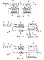
- FIGURE 4 diagrammatically illustrates pertinent portions of an exemplary transmitter apparatus (e.g. WCDMA or UMTS) for converting a baseband signal into an RF transmission signal according to the invention.
- a baseband signal 41 is input to an IF processing section 42 which combines the baseband signal with a further signal 43 produced by an IF frequency synthesizer 44.
- the signal 43 is provided at a frequency f LO (IF).
- the IF processing stage 42 outputs an IF signal to an RF processing stage 46 which combines the IF signal 45 with a further signal 47 produced by an RF frequency synthesizer 48.
- the signal 47 has a frequency designated in FIGURE 4 as f LO (RF).
- the RF processing section 46 outputs at 49 an RF transmission signal at a frequency f TX having a desired channel spacing, for example, 5 ⁇ n x 0.2 MHz.
- the IF frequency synthesizer 44 of FIGURE 4 includes the rastering capability that is conventionally provided in RF frequency synthesizers (see, for example, 18 in FIGURE 1). Because the frequency f LO (IF) of the signal 43 produced by the IF frequency synthesizer 44 is substantially lower than the frequency f LO (RF) of the signal 47 produced by the RF frequency synthesizer 48, the IF frequency synthesizer 44 can be advantageously used to provide the desired raster without requiring an undesirably large feedback divisor to produce the comparison frequency (which corresponds to the desired raster). Furthermore, because the raster is provided by the IF frequency synthesizer 44, the RF frequency synthesizer 48 can use any comparison frequency (designated as f compare in FIGURE 4) that is greater than the desired raster.
- FIGURE 5 diagrammatically illustrates an exemplary embodiment of the IF frequency synthesizer 44 of FIGURE 4.
- FIGURE 6 diagrammatically illustrates an exemplary embodiment of the RF frequency synthesizer 48 of FIGURE 4.
- the frequency synthesizer of FIGURE 6 is an integer PLL frequency synthesizer.
- the respective feedback divisors of the frequency synthesizers 44 and 48 are significantly lower than the feedback divisors associated with prior art arrangements such as shown in FIGURE 1, thus providing improved phase noise performance and faster locking as compared to prior art arrangements.
- the exemplary frequency synthesizer 48 is also implemented as a type-1 PLL.
- the available oscillator 21 of FIGURE 6 does not permit generation of a 5 MHz comparison frequency at 62 (for example a 13 MHz reference frequency from the oscillator 21 would not permit derivation of a 5 MHz comparison frequency if R is an integer), then another relatively high comparison frequency can be used.
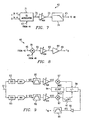
- FIGURES 7 and 8 diagrammatically illustrate exemplary embodiments of the IF processing section 42 and the RF processing section 46, respectively.
- the baseband I and Q signals are input to a conventional IQ modulator 71.
- the modulator 71 can utilize conventional techniques to combine the signal 43 (see Figure 4) with the baseband I and Q signals to produce an output signal 72 which is applied to a conventional variable gain amplifier (VGA).
- VGA variable gain amplifier
- the output 73 of the VGA is applied to a conventional low-pass filter 74 whose output is coupled to the RF processing section 46 of FIGURE 4.
- the embodiment of FIGURE 8 includes a conventional mixer 81 (for example, an SSB mixer or a DSB mixer) which receives the output 45 from the IF processing section 42 (see FIGURE 4).
- the mixer 81 mixes the IF signal 45 with the signal 47 produced by the RF frequency synthesizer 48 of FIGURE 4.
- the output 82 of the mixer 81 is provided to a conventional VGA whose output 83 is applied to a conventional power amplifier/driver 84 which provides the output signal 49 of FIGURE 4.
- FIGURE 9 illustrates another exemplary apparatus (e.g. WCDMA or UMTS) according to the invention for converting baseband signals into RF transmission signals.
- a modulating digital baseband signal at 91 is applied to a pair of DDS (direct digital synthesizer) sections at 93.
- the outputs of the DDS sections are input to respective digital-to-analog converters (DACs) to produce baseband I and Q signals also designated as S(f) in FIGURE 9.
- the I and Q signals are input to respective bandpass filters 95.
- the outputs of the filters 95 are input to respective VGAs, and the outputs of the VGAs are designated as S'(f) in FIGURE 9.
- the S'(f) components are input to respective mixers 97 which mix the respective components of S' (f) with a signal W(f) generated by a phase shifter 94.
- the phase shifter 94 produces the signal W(f) from, for example, the signal 47 produced by the RF frequency synthesizer 48 of FIGURE 6.
- the outputs of the mixers 97 are combined by a combiner 98 whose output is coupled to a power amplifier/driver 92 that produces a signal R(f).
- the signal R(f) is input to a bandpass filter 90, for example a SAW filter, that provides an output transmission signal having the frequency f TX and the desired channel spacing.
- the DDS sections 93 generate the desired (e.g., 200 KHz) raster.
- FIGURE 10 illustrates the frequency spectra of the signals S'(f), W(f) and R(f) of FIGURE 9.
- the signals I and Q corresponding to spectrum S'(f) are provided at a frequency of ⁇ IF ⁇ n x 0.2 MHz, where the "0.2" factor corresponds to the desired raster and the ⁇ IF component corresponds to the desired IF frequency.
- FIGURE 11 illustrates exemplary operations which can be performed by the embodiments of FIGURES 4-8.
- a signal at frequency ⁇ LO (IF) is produced using a comparison frequency corresponding to the desired raster.
- a signal at frequency ⁇ LO (RF) is produced using a comparison frequency that is greater than the desired raster.
- the signal at frequency ⁇ LO (IF) is combined with the baseband signal to produce an IF signal and, at 113, the signal at frequency ⁇ LO (RF) is combined with the IF signal to produce the desired RF transmission signal.
- FIGURE 12 illustrates exemplary operations which can be performed by the embodiments of FIGURES 4-10.
- an IF signal including the desired raster, is produced from the baseband signal.
- an RF signal is produced from the IF signal.
Landscapes
- Transmitters (AREA)
- Radar Systems Or Details Thereof (AREA)
- Reduction Or Emphasis Of Bandwidth Of Signals (AREA)
Abstract
Description
Claims (25)
- An apparatus for producing an RF transmission signal including a plurality of frequency channels, comprising:an IF processor having a first input for receiving a baseband signal and a second input for receiving a first combining signal, said IF processor for combining the baseband signal with the first combining signal to produce an IF signal;an RF processor having a first input coupled to said IF processor for receiving the IF signal and a second input for receiving a second combining signal, said RF processor for combining the IF signal with the second combining signal to produce an RF transmission signal including a plurality of frequency channels separated by a desired frequency channel spacing;a first frequency synthesizer coupled to said second input of said IF processor for providing the first combining signal at one of a plurality of possible frequencies separated from one another by a raster component of said desired frequency channel spacing; andsaid first frequency synthesizer including a comparison frequency generator for generating a comparison frequency corresponding to said raster component, said first frequency synthesizer responsive to said comparison frequency for producing the first combining signal.
- The apparatus of Claim 1, wherein the comparison frequency is an integer multiple of said raster component.
- The apparatus of Claim 1, wherein the comparison frequency is equal to said raster component.
- The apparatus of any preceding claim, wherein said first frequency synthesizer includes an integer phase locked loop.
- The apparatus of Claim 4, wherein said phase locked loop is a type -1
phase locked loop. - The apparatus of any one of Claims 1-5, provided in a UMTS
transmitter. - The apparatus of any one of Claims 1-5, provided in a WCDMA transmitter.
- The apparatus of any one of Claims 1-7, including a second frequency synthesizer coupled to said second input of said RF processor for providing the second combining signal, said second frequency synthesizer including a further comparison frequency generator for generating a further comparison frequency that is greater than said raster component, said second frequency synthesizer responsive to said further comparison frequency for producing the second combining signal.
- The apparatus of Claim 8, wherein the further comparison frequency corresponds to a further component of said desired frequency channel spacing other than said raster component.
- The apparatus of Claim 8 or Claim 9, wherein said second frequency synthesizer includes an integer phase locked loop.
- A method for producing an RF transmission signal including a plurality of frequency channels separated by a desired frequency channel spacing, comprising:providing a first combining signal at one of a plurality of possible frequencies separated from one another by a raster component of the desired frequency channel spacing, including generating a comparison frequency corresponding to said raster component and producing the first combining signal in response to said comparison frequency;combining the first combining signal with a baseband signal to produce an IF signal; andcombining the IF signal with a second combining signal to produce the RF transmission signal.
- The method of Claim 11, wherein the comparison frequency is an integer multiple of said raster component.
- The method of Claims 11 or 12, wherein the comparison frequency is equal to said raster component.
- The method of any one of Claims 11-13, wherein said providing step includes using an integer phase locked loop to produce the first combining signal.
- The method of Claim 14, wherein said using step includes using a type-1 phase locked loop to produce the first combining signal.
- The method of any one of Claims 11-15, wherein the RF transmission signal is a UMTS transmission signal.
- The method of any one of Claims 11-15, wherein the RF transmission signal is a WCDMA transmission signal.
- The method of any one of Claims 11-17, including generating a further comparison frequency that is greater than said raster component, and producing the second combining signal in response to said further comparison frequency.
- The method of Claim 18, wherein the further comparison frequency corresponds to a further component of said desired frequency channel spacing other than said raster component.
- The method of Claim 18, wherein said step of producing the second combining signal includes using an integer phase locked loop to produce the second combining signal.
- An apparatus for producing an RF transmission signal including a plurality of frequency channels separated by a desired frequency channel spacing, comprising:an input for receiving a baseband signal;an IF processor coupled to said input for receiving said baseband signal and producing therefrom an IF signal including a raster component of said desired frequency channel spacing; andan RF processor coupled to said IF processor for receiving the IF signal and producing therefrom said RF transmission signal.
- The apparatus of Claim 21, wherein said IF processor includes a direct digital synthesizer.
- The apparatus of Claim 21, provided in one of a UMTS transmitter and a WCDMA transmitter.
- A method for producing an RF transmission signal including a plurality of frequency channels separated by a desired frequency channel spacing, comprising:producing from a baseband signal an IF signal including a raster component of said desired frequency channel spacing; andproducing the RF transmission signal from the IF signal.
- The method of Claim 24, wherein the RF transmission signal is one of a UMTS transmission signal and a WCDMA transmission signal.
Applications Claiming Priority (2)
| Application Number | Priority Date | Filing Date | Title |
|---|---|---|---|
| US706068 | 1985-02-27 | ||
| US09/706,068 US6990154B1 (en) | 2000-11-03 | 2000-11-03 | Using an IF synthesizer to provide raster component of frequency channel spacing |
Publications (3)
| Publication Number | Publication Date |
|---|---|
| EP1204201A2 true EP1204201A2 (en) | 2002-05-08 |
| EP1204201A3 EP1204201A3 (en) | 2004-05-26 |
| EP1204201B1 EP1204201B1 (en) | 2008-11-05 |
Family
ID=24836100
Family Applications (1)
| Application Number | Title | Priority Date | Filing Date |
|---|---|---|---|
| EP01000592A Expired - Lifetime EP1204201B1 (en) | 2000-11-03 | 2001-11-02 | Apparatus and method for producing an RF transmision signal |
Country Status (5)
| Country | Link |
|---|---|
| US (1) | US6990154B1 (en) |
| EP (1) | EP1204201B1 (en) |
| JP (1) | JP2002198832A (en) |
| AT (1) | ATE413721T1 (en) |
| DE (1) | DE60136432D1 (en) |
Families Citing this family (1)
| Publication number | Priority date | Publication date | Assignee | Title |
|---|---|---|---|---|
| US7613430B1 (en) * | 2005-12-22 | 2009-11-03 | Atheros Communications, Inc. | Dual synthesizer RF frequency plan optimized for interference avoidance |
Family Cites Families (7)
| Publication number | Priority date | Publication date | Assignee | Title |
|---|---|---|---|---|
| US5722040A (en) * | 1993-02-04 | 1998-02-24 | Pacific Communication Sciences, Inc. | Method and apparatus of frequency generation for use with digital cordless telephones |
| FI941862A7 (en) | 1994-04-21 | 1995-10-22 | Nokia Mobile Phones Ltd | Method and radio frequency system for forming the frequencies of a receiver and transmitter of two radio communication systems operating in different frequency ranges, and a receiver and transmitter operating in two different frequency ranges, and use of the foregoing in a mobile phone |
| JPH09233143A (en) | 1996-02-26 | 1997-09-05 | Nec Corp | Digital wireless communication device |
| EP0940922B1 (en) * | 1998-03-03 | 2002-12-04 | Motorola Semiconducteurs S.A. | Frequency synthesiser |
| US6091303A (en) * | 1999-04-06 | 2000-07-18 | Ericsson Inc. | Method and apparatus for reducing oscillator noise by noise-feedforward |
| US6556545B1 (en) * | 1999-12-21 | 2003-04-29 | Ericsson Inc. | Frequency generation for CDMA terminal with slotted receive mode |
| US6463112B1 (en) * | 2000-05-25 | 2002-10-08 | Research In Motion Limited | Phase locked-loop using sub-sampling |
-
2000
- 2000-11-03 US US09/706,068 patent/US6990154B1/en not_active Expired - Lifetime
-
2001
- 2001-11-02 AT AT01000592T patent/ATE413721T1/en not_active IP Right Cessation
- 2001-11-02 EP EP01000592A patent/EP1204201B1/en not_active Expired - Lifetime
- 2001-11-02 DE DE60136432T patent/DE60136432D1/en not_active Expired - Lifetime
- 2001-11-02 JP JP2001337889A patent/JP2002198832A/en not_active Withdrawn
Also Published As
| Publication number | Publication date |
|---|---|
| ATE413721T1 (en) | 2008-11-15 |
| JP2002198832A (en) | 2002-07-12 |
| US6990154B1 (en) | 2006-01-24 |
| EP1204201A3 (en) | 2004-05-26 |
| DE60136432D1 (en) | 2008-12-18 |
| EP1204201B1 (en) | 2008-11-05 |
Similar Documents
| Publication | Publication Date | Title |
|---|---|---|
| US7394874B2 (en) | Up/down conversion circuitry for radio transceiver | |
| US7003274B1 (en) | Frequency synthesizer and synthesis method for generating a multiband local oscillator signal | |
| US6915117B2 (en) | Multistage modulation architecture and method in a radio | |
| KR102077620B1 (en) | Low Phase Noise Ultra-wideband Frequency Synthesizer and Frequency Synthesizer method | |
| EP2064814B1 (en) | Digital polar radiofrequency transmitting device with a radiofrequency reference oscillator and an integrated circuit comprising such device | |
| US8902953B2 (en) | RF digital spur reduction | |
| CN1890993A (en) | Multi-system mode and multi-band radio frequency transmitter receiver and related communication method | |
| US8682273B2 (en) | RF digital spur reduction | |
| KR100997491B1 (en) | Communication transmitter using offset phase locked loop | |
| US5712602A (en) | Phase-locked oscillator for microwave/millimeter-wave ranges | |
| US7471934B2 (en) | Transmitter method, apparatus, and frequency plan for minimizing spurious energy | |
| US7949072B2 (en) | Local oscillator with injection pulling suppression and spurious products filtering | |
| US6519305B1 (en) | Frequency converter arrangement | |
| US20080125060A1 (en) | Radio Frequency Transceiver | |
| US6990154B1 (en) | Using an IF synthesizer to provide raster component of frequency channel spacing | |
| US6952593B2 (en) | Multi-band tranceivers with reduced frequency sources for digital transmissions | |
| EP1217723A2 (en) | Quadrature modulator using a Phase Locked Loop | |
| EP2579454A2 (en) | Apparatus generating subcarrier for transmission between ultra-high frequency channels and method generating the same | |
| US6347219B1 (en) | Transmission system, transmission/reception system, and local oscillator to be used in the same | |
| JPH07235893A (en) | Method and apparatus for forming intermediate frequency signal for wireless telephone | |
| GB2325362A (en) | Transceiver which uses transmission signal as local oscillator for reception | |
| JPS63102419A (en) | Microwave band frequency synthesizer | |
| JPH06104778A (en) | Wireless transmitter | |
| CN116865750A (en) | Broadband agile frequency acquisition method and synthesizer | |
| JPH05191302A (en) | Wireless transmitter |
Legal Events
| Date | Code | Title | Description |
|---|---|---|---|
| PUAI | Public reference made under article 153(3) epc to a published international application that has entered the european phase |
Free format text: ORIGINAL CODE: 0009012 |
|
| AK | Designated contracting states |
Kind code of ref document: A2 Designated state(s): AT BE CH CY DE DK ES FI FR GB GR IE IT LI LU MC NL PT SE TR |
|
| AX | Request for extension of the european patent |
Free format text: AL;LT;LV;MK;RO;SI |
|
| PUAL | Search report despatched |
Free format text: ORIGINAL CODE: 0009013 |
|
| AK | Designated contracting states |
Kind code of ref document: A3 Designated state(s): AT BE CH CY DE DK ES FI FR GB GR IE IT LI LU MC NL PT SE TR |
|
| AX | Request for extension of the european patent |
Extension state: AL LT LV MK RO SI |
|
| 17P | Request for examination filed |
Effective date: 20041126 |
|
| AKX | Designation fees paid |
Designated state(s): AT BE CH CY DE DK ES FI FR GB GR IE IT LI LU MC NL PT SE TR |
|
| GRAP | Despatch of communication of intention to grant a patent |
Free format text: ORIGINAL CODE: EPIDOSNIGR1 |
|
| GRAS | Grant fee paid |
Free format text: ORIGINAL CODE: EPIDOSNIGR3 |
|
| GRAA | (expected) grant |
Free format text: ORIGINAL CODE: 0009210 |
|
| AK | Designated contracting states |
Kind code of ref document: B1 Designated state(s): AT BE CH CY DE DK ES FI FR GB GR IE IT LI LU MC NL PT SE TR |
|
| REG | Reference to a national code |
Ref country code: GB Ref legal event code: FG4D |
|
| REG | Reference to a national code |
Ref country code: CH Ref legal event code: EP |
|
| REG | Reference to a national code |
Ref country code: IE Ref legal event code: FG4D |
|
| REF | Corresponds to: |
Ref document number: 60136432 Country of ref document: DE Date of ref document: 20081218 Kind code of ref document: P |
|
| PG25 | Lapsed in a contracting state [announced via postgrant information from national office to epo] |
Ref country code: AT Free format text: LAPSE BECAUSE OF FAILURE TO SUBMIT A TRANSLATION OF THE DESCRIPTION OR TO PAY THE FEE WITHIN THE PRESCRIBED TIME-LIMIT Effective date: 20081105 Ref country code: ES Free format text: LAPSE BECAUSE OF FAILURE TO SUBMIT A TRANSLATION OF THE DESCRIPTION OR TO PAY THE FEE WITHIN THE PRESCRIBED TIME-LIMIT Effective date: 20090216 |
|
| PG25 | Lapsed in a contracting state [announced via postgrant information from national office to epo] |
Ref country code: FI Free format text: LAPSE BECAUSE OF FAILURE TO SUBMIT A TRANSLATION OF THE DESCRIPTION OR TO PAY THE FEE WITHIN THE PRESCRIBED TIME-LIMIT Effective date: 20081105 |
|
| PG25 | Lapsed in a contracting state [announced via postgrant information from national office to epo] |
Ref country code: DK Free format text: LAPSE BECAUSE OF FAILURE TO SUBMIT A TRANSLATION OF THE DESCRIPTION OR TO PAY THE FEE WITHIN THE PRESCRIBED TIME-LIMIT Effective date: 20081105 Ref country code: BE Free format text: LAPSE BECAUSE OF FAILURE TO SUBMIT A TRANSLATION OF THE DESCRIPTION OR TO PAY THE FEE WITHIN THE PRESCRIBED TIME-LIMIT Effective date: 20081105 |
|
| PG25 | Lapsed in a contracting state [announced via postgrant information from national office to epo] |
Ref country code: PT Free format text: LAPSE BECAUSE OF FAILURE TO SUBMIT A TRANSLATION OF THE DESCRIPTION OR TO PAY THE FEE WITHIN THE PRESCRIBED TIME-LIMIT Effective date: 20090406 Ref country code: SE Free format text: LAPSE BECAUSE OF FAILURE TO SUBMIT A TRANSLATION OF THE DESCRIPTION OR TO PAY THE FEE WITHIN THE PRESCRIBED TIME-LIMIT Effective date: 20090205 |
|
| PLBE | No opposition filed within time limit |
Free format text: ORIGINAL CODE: 0009261 |
|
| STAA | Information on the status of an ep patent application or granted ep patent |
Free format text: STATUS: NO OPPOSITION FILED WITHIN TIME LIMIT |
|
| 26N | No opposition filed |
Effective date: 20090806 |
|
| PG25 | Lapsed in a contracting state [announced via postgrant information from national office to epo] |
Ref country code: MC Free format text: LAPSE BECAUSE OF NON-PAYMENT OF DUE FEES Effective date: 20091130 |
|
| REG | Reference to a national code |
Ref country code: CH Ref legal event code: PL |
|
| REG | Reference to a national code |
Ref country code: IE Ref legal event code: MM4A |
|
| PG25 | Lapsed in a contracting state [announced via postgrant information from national office to epo] |
Ref country code: LI Free format text: LAPSE BECAUSE OF NON-PAYMENT OF DUE FEES Effective date: 20091130 Ref country code: IE Free format text: LAPSE BECAUSE OF NON-PAYMENT OF DUE FEES Effective date: 20091102 Ref country code: GR Free format text: LAPSE BECAUSE OF FAILURE TO SUBMIT A TRANSLATION OF THE DESCRIPTION OR TO PAY THE FEE WITHIN THE PRESCRIBED TIME-LIMIT Effective date: 20090206 Ref country code: CH Free format text: LAPSE BECAUSE OF NON-PAYMENT OF DUE FEES Effective date: 20091130 |
|
| PG25 | Lapsed in a contracting state [announced via postgrant information from national office to epo] |
Ref country code: IT Free format text: LAPSE BECAUSE OF FAILURE TO SUBMIT A TRANSLATION OF THE DESCRIPTION OR TO PAY THE FEE WITHIN THE PRESCRIBED TIME-LIMIT Effective date: 20081105 |
|
| PG25 | Lapsed in a contracting state [announced via postgrant information from national office to epo] |
Ref country code: LU Free format text: LAPSE BECAUSE OF NON-PAYMENT OF DUE FEES Effective date: 20091102 |
|
| PG25 | Lapsed in a contracting state [announced via postgrant information from national office to epo] |
Ref country code: TR Free format text: LAPSE BECAUSE OF FAILURE TO SUBMIT A TRANSLATION OF THE DESCRIPTION OR TO PAY THE FEE WITHIN THE PRESCRIBED TIME-LIMIT Effective date: 20081105 |
|
| PG25 | Lapsed in a contracting state [announced via postgrant information from national office to epo] |
Ref country code: CY Free format text: LAPSE BECAUSE OF FAILURE TO SUBMIT A TRANSLATION OF THE DESCRIPTION OR TO PAY THE FEE WITHIN THE PRESCRIBED TIME-LIMIT Effective date: 20081105 |
|
| REG | Reference to a national code |
Ref country code: FR Ref legal event code: PLFP Year of fee payment: 15 |
|
| REG | Reference to a national code |
Ref country code: FR Ref legal event code: PLFP Year of fee payment: 16 |
|
| PGFP | Annual fee paid to national office [announced via postgrant information from national office to epo] |
Ref country code: GB Payment date: 20161026 Year of fee payment: 16 Ref country code: DE Payment date: 20161130 Year of fee payment: 16 Ref country code: NL Payment date: 20161107 Year of fee payment: 16 Ref country code: FR Payment date: 20161017 Year of fee payment: 16 |
|
| REG | Reference to a national code |
Ref country code: DE Ref legal event code: R119 Ref document number: 60136432 Country of ref document: DE |
|
| REG | Reference to a national code |
Ref country code: NL Ref legal event code: MM Effective date: 20171201 |
|
| GBPC | Gb: european patent ceased through non-payment of renewal fee |
Effective date: 20171102 |
|
| REG | Reference to a national code |
Ref country code: FR Ref legal event code: ST Effective date: 20180731 |
|
| PG25 | Lapsed in a contracting state [announced via postgrant information from national office to epo] |
Ref country code: DE Free format text: LAPSE BECAUSE OF NON-PAYMENT OF DUE FEES Effective date: 20180602 Ref country code: FR Free format text: LAPSE BECAUSE OF NON-PAYMENT OF DUE FEES Effective date: 20171130 Ref country code: NL Free format text: LAPSE BECAUSE OF NON-PAYMENT OF DUE FEES Effective date: 20171201 |
|
| PG25 | Lapsed in a contracting state [announced via postgrant information from national office to epo] |
Ref country code: GB Free format text: LAPSE BECAUSE OF NON-PAYMENT OF DUE FEES Effective date: 20171102 |