EP1204199A2 - Mains frequency synchronous burst mode power supply - Google Patents
Mains frequency synchronous burst mode power supply Download PDFInfo
- Publication number
- EP1204199A2 EP1204199A2 EP01113054A EP01113054A EP1204199A2 EP 1204199 A2 EP1204199 A2 EP 1204199A2 EP 01113054 A EP01113054 A EP 01113054A EP 01113054 A EP01113054 A EP 01113054A EP 1204199 A2 EP1204199 A2 EP 1204199A2
- Authority
- EP
- European Patent Office
- Prior art keywords
- voltage
- circuit
- power supply
- pulses
- coupled
- Prior art date
- Legal status (The legal status is an assumption and is not a legal conclusion. Google has not performed a legal analysis and makes no representation as to the accuracy of the status listed.)
- Withdrawn
Links
Images


Classifications
-
- H—ELECTRICITY
- H04—ELECTRIC COMMUNICATION TECHNIQUE
- H04N—PICTORIAL COMMUNICATION, e.g. TELEVISION
- H04N5/00—Details of television systems
- H04N5/63—Generation or supply of power specially adapted for television receivers
-
- H—ELECTRICITY
- H02—GENERATION; CONVERSION OR DISTRIBUTION OF ELECTRIC POWER
- H02M—APPARATUS FOR CONVERSION BETWEEN AC AND AC, BETWEEN AC AND DC, OR BETWEEN DC AND DC, AND FOR USE WITH MAINS OR SIMILAR POWER SUPPLY SYSTEMS; CONVERSION OF DC OR AC INPUT POWER INTO SURGE OUTPUT POWER; CONTROL OR REGULATION THEREOF
- H02M3/00—Conversion of DC power input into DC power output
- H02M3/22—Conversion of DC power input into DC power output with intermediate conversion into AC
- H02M3/24—Conversion of DC power input into DC power output with intermediate conversion into AC by static converters
- H02M3/28—Conversion of DC power input into DC power output with intermediate conversion into AC by static converters using discharge tubes with control electrode or semiconductor devices with control electrode to produce the intermediate AC
- H02M3/325—Conversion of DC power input into DC power output with intermediate conversion into AC by static converters using discharge tubes with control electrode or semiconductor devices with control electrode to produce the intermediate AC using devices of a triode or a transistor type requiring continuous application of a control signal
- H02M3/335—Conversion of DC power input into DC power output with intermediate conversion into AC by static converters using discharge tubes with control electrode or semiconductor devices with control electrode to produce the intermediate AC using devices of a triode or a transistor type requiring continuous application of a control signal using semiconductor devices only
- H02M3/33507—Conversion of DC power input into DC power output with intermediate conversion into AC by static converters using discharge tubes with control electrode or semiconductor devices with control electrode to produce the intermediate AC using devices of a triode or a transistor type requiring continuous application of a control signal using semiconductor devices only with automatic control of the output voltage or current, e.g. flyback converters
- H02M3/33523—Conversion of DC power input into DC power output with intermediate conversion into AC by static converters using discharge tubes with control electrode or semiconductor devices with control electrode to produce the intermediate AC using devices of a triode or a transistor type requiring continuous application of a control signal using semiconductor devices only with automatic control of the output voltage or current, e.g. flyback converters with galvanic isolation between input and output of both the power stage and the feedback loop
-
- H—ELECTRICITY
- H02—GENERATION; CONVERSION OR DISTRIBUTION OF ELECTRIC POWER
- H02M—APPARATUS FOR CONVERSION BETWEEN AC AND AC, BETWEEN AC AND DC, OR BETWEEN DC AND DC, AND FOR USE WITH MAINS OR SIMILAR POWER SUPPLY SYSTEMS; CONVERSION OF DC OR AC INPUT POWER INTO SURGE OUTPUT POWER; CONTROL OR REGULATION THEREOF
- H02M1/00—Details of apparatus for conversion
- H02M1/0003—Details of control, feedback or regulation circuits
- H02M1/0032—Control circuits allowing low power mode operation, e.g. in standby mode
- H02M1/0035—Control circuits allowing low power mode operation, e.g. in standby mode using burst mode control
-
- Y—GENERAL TAGGING OF NEW TECHNOLOGICAL DEVELOPMENTS; GENERAL TAGGING OF CROSS-SECTIONAL TECHNOLOGIES SPANNING OVER SEVERAL SECTIONS OF THE IPC; TECHNICAL SUBJECTS COVERED BY FORMER USPC CROSS-REFERENCE ART COLLECTIONS [XRACs] AND DIGESTS
- Y02—TECHNOLOGIES OR APPLICATIONS FOR MITIGATION OR ADAPTATION AGAINST CLIMATE CHANGE
- Y02B—CLIMATE CHANGE MITIGATION TECHNOLOGIES RELATED TO BUILDINGS, e.g. HOUSING, HOUSE APPLIANCES OR RELATED END-USER APPLICATIONS
- Y02B70/00—Technologies for an efficient end-user side electric power management and consumption
- Y02B70/10—Technologies improving the efficiency by using switched-mode power supplies [SMPS], i.e. efficient power electronics conversion e.g. power factor correction or reduction of losses in power supplies or efficient standby modes
Definitions
- This invention relates generally to the field of power supplies, and, in particular, to standby mode power supplies for television receivers.
- the power consumed by electronic equipment in the standby mode is becoming an increasingly visible public policy issue.
- an article in the September 19, 1997, issue of Europe Energy reports that the European Commission regards reducing the energy consumed by electronic equipment in the standby mode of operation as a priority.
- the article further states that the Commission has concentrated its initial efforts at reducing the standby power consumption of televisions and VCRs, and that it has elicited voluntary commitments from manufacturers of such products to progressively reduce average standby power consumption.
- Modern televisions can have a standby power consumption of about 5 to 10 Watts caused by the degaussing circuit and switched mode power supply running in standby mode. Televisions that have an additional standby power supply and disconnect the degaussing circuit can reduce the power consumption to 1 Watt.
- a primary winding of a standby transformer is coupled to the AC mains.
- a transformed voltage across a secondary winding of the standby transformer is full-wave rectified and is regulated by some form of linear regulation to provide power for the video display apparatus in a standby mode of operation.
- This standby power supply consumes power as long as the video display apparatus is connected to the AC mains, and thus also consumes power during the run mode of operation. During standby mode, power losses are incurred partly due to switching losses.
- U.S. patent no. 6,043,994 proposes a power supply for reducing standby power consumption attributable to a start-up resistor of the switched mode power supply controller integrated circuit IC.
- a synchronous burst mode power supply includes a power converter for transforming an AC mains from a relatively low frequency to a higher frequency; and a gate circuit responsive to the AC mains supply for enabling the power converter to initiate a burst of output pulses at the higher frequency each time the AC mains supply occurs within a predetermined range.
- a method for providing synchronous burst mode power includes the steps of receiving an AC mains supply at a relatively low frequency, detecting when the AC mains supply occurs within a predetermined range, and initiating a burst of output pulses at a higher frequency than the relatively low frequency in response to the detecting step.
- Resistors values shown are in units of measure indicated as ohms, kilo-ohms (k), or Mega-ohms (M), and capacitor values are in units of measure indicated as microfarads (u) or picofarads (p).
- the present invention reduces power losses associated with circuit switching in a standby switched mode power supply SMPS.
- the inventive standby SMPS is connected directly to a rippled but rectified mains voltage, which is then gated to the SMPS during periods of low levels of the rectified mains voltage. Gating of the rectified mains voltage to the standby SMPS, which responds by generating burst pulses, is synchronous with a predetermined range in the rectified mains voltage.
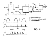
- a mains voltage Vmains is rectified by a diode D1 to provide rippled and positive half wave voltages V1 to a threshold detector 1.
- Voltage pulses V2 are output by the threshold detector 1 when the rise and fall of the positive half wave voltages V1 are below a threshold level (horizontal line 16 in graph 11 of FIG.1).
- the voltage pulses V2 at the relatively low frequency of the mains voltage Vmains, for example 50 or 60 Hz, are converted by the free running oscillator 23 to sawtooth current pulses ITr at a higher frequency.
- the detector acts as a gate with respect to passing part of the positive half-waves to the oscillator circuit 23.
- the Ac mains voltage alone initiates and terminates the burst pulses V2, independent of any external switching control.
- nine sawtooth pulses ITr are generated for every voltage pulse V2 output by the detector 1. This number is related to the free running frequency of the oscillator, for example 25 kHz. Peaks of the sawtooth current pulses decrease in a linear sloping manner, as shown, because the positive half-wave pulse V1 imposed on the transformer Tr1 decreases from its peak to zero. Voltage imposed on a transformer follows the relationship (voltage /inductance) multiplied by time. In the present circuit the time factor is constant but the mains sine wave voltage increases from zero to a peak value and then decreases from its peak value to zero. The decrease from peak value to zero causes the linear decaying peaks in the sawtooth current pulses ITr. Conversely, during the rising edge of the mains voltage sine wave the peaks of the sawtooth current pulses ITr rise linearly.
- the sawtooth current pulses ITr are transformed into a secondary winding voltage VTR1, which is then diode D7 rectified into an unregulated voltage V3.
- the unregulated voltage V3 is smoothed and regulated by a voltage regulator 3 to an output voltage Vout of 5V DC.
- An exemplary circuit in FIG. 2 includes a circuit arrangement 20 for controllably coupling the voltage mains Vmains over to a connection point for a run mode power supply (not shown).
- the voltage mains Vmains is switched across an opto-relay, Triac T2, responding to a run control signal through current limiting resistor R13 from a known type of microcontroller (not shown).
- Alternative relay switches in lieu of triac driver T2 can be employed.
- the voltage Vmains is also coupled across a triac T1 triggered when the mains voltage is passed by the triac driver T2 and dropped across a voltage divider made up by resistors R11 and R12.
- the voltage mains Vmains passed by triac T1 is coupled across a degaussing circuit 21, full wave rectified by a diode bridge arrangement D11-D14 and filtered by capacitor C11 for a run mode power supply.
- the circuit embodiment of FIG. 2 further includes exemplary circuit embodiments for the threshold detector 1, free running oscillator 2 and voltage stabilizer 3.
- Positive half wave voltages V1 from the voltage mains Vmains rectified by diode D1 are voltage divided between resistors R4 and R5, voltage limited by zener diode D3, and ripple attenuated by capacitor C1 to provide +12V to the emitter terminal E of transistor Q1.
- Transistor Q1 is biased by voltage developed at its base terminal B from the rectifier arrangement of voltage divider resistors R1 and R3 and filtering capacitor C2.
- An optional adjustable resistor R2 allows for fine adjustment of the base terminal B voltage.
- Transistor Q1 is protected by diode D2 against a possible reverse biasing due to the +12V developed at the emitter terminal E of transistor Q1.
- transistor Q1 When the input voltage to the base terminal B of transistor Q1 is below a certain threshold, determined by the emitter E voltage of transistor Q1 and the voltage divider R4, R5 and D3, transistor Q1 turns on and provides the free running oscillator circuit 23 with a bias voltage. It is noted that resistor R5 adapts the on-time of the oscillator circuit 23 to different mains voltages.
- +12V at the positive terminal of capacitor C1 is compared with voltage at the base terminal B of transistor Q1.
- a positive voltage at terminal B of transistor Q1 greater than 0 and less than about 11.3 volts biases transistor Q1 on, providing the threshold level 16 of about 11.3 volts. Above 11.3 volts at base terminal B, PNP transistor Q1 is biased off.
- the threshold detector or gate circuit 22 provides low voltage level switching which reduces losses otherwise present in a typical switched mode standby power supply.
- the oscillator 23 in FIG. 2 is a blocking oscillator formed by transformer Tr1, resistor R6, capacitor C3, secondary winding n3 and transistor Q2.
- the blocking oscillator operates in a conventional manner. It is noted that diodes D4 and D5 and resistor R7 are not necessary for basic operation of the oscillator circuit, but have been included as one form of signal conditioning.
- the depiction of blocking oscillator circuit 23 is merely exemplary and does not proscribe the use of other oscillator circuits or topologies in the context of the present invention.
- Positive feedback provided by secondary winding n3 keeps transistor Q2 conducting.
- Current through base terminal B of transistor Q2 keeps capacitor C3 discharging until the voltage across the capacitor C3 is 1.4V, at which point transistor Q2 stops conducting and power is transferred to the secondary side via winding n2 in a flyback manner.
- capacitor C3 is pulled down to negative.
- current has to be fed through resistor R6 again to charge up capacitor C3 and start conduction of another saw tooth current ITR, derived from the positive half-wave pulses V1.
- Capacitor C4 reduces radiation of the fast switching.
- the blocking oscillator 23 runs with an almost constant frequency that is dependent on the voltage Vmains, resistor R6, capacitor C3 and the relationship between windings n1 and n3.
- the duty cycle of the oscillation can be substantially constant so that the energy transferred to the secondary winding n2 is substantially constant.
- This substantially constant energy has two consequences.
- Second, parallel voltage regulation techniques can be used to regulate the voltages provided by the secondary windings n2.
- the +5V output provided by the secondary winding n2 can be partly limited by zener diode D7 and regulated by the voltage regulator IC1.
- the use of voltage regulator IC1 and diode D7 is merely illustrative and does not preclude the applicability of other voltage regulation techniques in the context of the present invention.
- the blocking oscillator 23 is advantageously used to transform the relatively low mains voltage frequency, for example 50 to 60 Hz, from which two voltage pulses V2 appear per cycle to a frequency from which nine sawtooth current pulses are generated for each voltage pulse V2.
- This transformation permits a decrease in the size of standby transformer Tr1, which in turn, leads to a decrease in the power consumption by the standby transformer Tr1.
- the secondary winding voltage VTR1 reaching 7.2V in the exemplary circuit, is initially rectified by diode D5, filtered by capacitor C5 and then regulated by the voltage regulator IC1. In case of reload, diode D7 prevents capacitor C5 and voltage regulator IC1 from too much voltage. Voltage output by the regulator IC is filtered by capacitor C6 to provide the +5V standby power.
- the circuit of FIG. 3 is similar to the standby power arrangement of FIG. 2, except for the current feedback loop from an additional opto-coupler IC2 coupled to the terminal between resistor R5 and zener diode D3 of the threshold detector circuit 22.
- the circuit embodiment of FIG. 2 is suited for a static load or a relatively small variation in load where resistor R2 can be adjusted to optimally time the initiation and termination of burst pulses suitable for the load amount. If R2 is optimally adjusted for a certain load and the actual load is relatively small then the burst pulse frequency will be too high and the power output will be greater than needed for the load, resulting in wasted power. Dynamic load applications are appropriate for the circuit embodiment of FIG. 3, where the current feedback adjusts the initiation and termination of burst pulses V2 by the gate circuit.
- the current feedback loop of FIG. 3 eliminates the need for the variable resistor R2 adjustment of FIG. 2.
- the opto-coupler IC2 conducts whenever secondary voltage V3 is above a reference voltage developed across D7. Conduction by the opto-coupler IC2 reduces the reference voltage for the emitter of transistor Q1 via current I1 in the feedback loop, which reduces the on time of the free running oscillator circuit 22. As a consequence, the input power is reduced when load decreases, and the voltage controlling potentiometer R2 in the circuit embodiment of FIG. 2 is unnecessary.
- FIG. 4 is a graph of the range of input power versus output power demonstrating the increased efficiency provided by the invention.
- An ordinary power supply will ordinarily consume 1W to output 200 mW, representing a 20% power conversion efficiency.
- As the graph of FIG. 4 demonstrates, for example, that with the inventive gating on of momentary low voltage mains an input mains voltage power Pinput of approximately 337 mW is converted to standby power of approximately 115 mW. This represents an increase in power conversion efficiency to approximately 30%.
- the standby transformer TR1 may be constructed using an EF16, N67 core with an air gap equal to approximately 0.1 mm.
- the inductance of the primary winding n1 of the standby transformer Tr1 may be equal to approximately 18 mH, using approximately 160 turns, in two layers, of 0.1 mm diameter CuL wire.
- Approximately one layer of 0.1 mm thickness MYLAR® brand polymeric film may be used to provide electrical isolation between the two layers of wire to reduce parasitic capacitance.
- the secondary winding n2 may use 23 turns of 0.315 mm diameter CuL wire, and the secondary winding n3 may use 16 turns of 0.315 mm diameter wire.
- Approximately 2 layers of 0.1 mm thickness MYLAR® brand polymeric film may be used to provide electrical isolation between the primary winding n1 and the secondary windings n2 and n3.
Landscapes
- Engineering & Computer Science (AREA)
- Power Engineering (AREA)
- Multimedia (AREA)
- Signal Processing (AREA)
- Dc-Dc Converters (AREA)
- Ac-Ac Conversion (AREA)
- Rectifiers (AREA)
Abstract
Description
Claims (25)
- A synchronous burst mode power supply comprising:a power converter (2) for transforming an AC mains from a relatively low frequency to a higher frequency; anda gate circuit (1) responsive to said AC mains supply for enabling said power converter (2) to initiate a burst of output pulses at said higher frequency each time said AC mains supply occurs within a predetermined range.
- The power supply according to claim 1, further comprising means (3) for regulating a transformed output (V3) from said converter circuit (2) to a standby voltage (Vout), said means (3) being coupled back to said gate circuit (1) for controlling operation of said power converter circuit (2) in response to load changes to said power supply.
- The power supply according to claim 1, wherein said power converter (2) comprises a self-oscillating circuit (Block 2) and said gate circuit (Block 1) enables operation of said self-oscillating circuit only during two periods of each cycle of said supply (V1) from said AC mains when said supply (V1) has a single voltage polarity.
- The power supply according to claim 1, wherein said gate circuit comprises a threshold detector circuit (22) for generating voltage pulses (V2) when detecting portions of positive waveforms (V1) of said mains voltage within said predetermined range.
- The power supply according to claim 4, wherein said threshold detector (22) comprises a transistor (Q1) biased at its base terminal by a first voltage division (R1, R2) of said positive waveforms (V1) to pass said voltage pulses (V2) from a second voltage division of said positive waveforms (V1).
- The power supply circuit of Claim 5, wherein said first voltage division comprises a resistor pair (R1, R3) divider coupled to a base terminal B of said transistor (Q1), and said second voltage division comprises a resistor pair (R4, R5) coupled to said positive waveforms (V1) and an emitter terminal of said transistor (Q1).
- The power supply circuit of Claim 4, wherein said power converter circuit (2) comprises a free running oscillator circuit (23) for converting said voltage pulses (V2) from said gate circuit (1) at a first frequency to current pulses (ITr) at a second frequency greater than said first frequency.
- The power supply circuit of Claim 7, wherein said free running oscillator circuit (23) comprises a transistor (Q2) biased at its base terminal B by said voltage pulses (V2) that are rectified by a first diode and then charge a first capacitor (C3) for enabling said second transistor (Q2) to conduct said current pulses (ITr), said current pulses (ITr) being derived from said positive waveforms (V1) ripple attenuated by a second capacitor (C4) coupled to an emitter terminal of said second transistor (Q2), said positive waveforms (V1) energizing a primary winding (n1) of a transformer (TR1) to develop in a flyback manner a secondary winding voltage (VTR1) across a secondary winding (n2) of said transformer (TR1).
- The power supply circuit of Claim 7, further comprising a voltage regulating circuit (24) coupled to a secondary winding (n2) of a transformer (TR1) having a primary winding (n1) coupled to said free running oscillator circuit (2), said secondary winding (n2) developing a secondary voltage (VTR1) from said current pulses(ITr) conducted through a primary winding (n1) of said transformer (TR1).
- The power supply circuit of Claim 9, wherein said voltage regulating circuit (24) comprises an integrated voltage regulator (IC1) coupled to a diode D6 and a first capacitor (C5) arrangement for rectifying and filtering said current pulses (ITr) from said secondary winding (n2) to provide a secondary voltage (V3) stabilized by said integrated voltage regulator (IC1), said secondary voltage being filtered by a second capacitor (C6) to provide a standby voltage (Vout).
- The power supply circuit of Claim 7, further comprising a voltage regulating circuit (244) coupled to a secondary winding (n2) of a transformer (TR1) having a primary winding (n1) through which said current pulses (ITr) controllably conduct to develop a secondary winding voltage (VTR1) that is coupled back to and adjust on-time operation of said threshold detector circuit (222).
- A synchronous burst mode standby power supply comprising:a self-oscillating power converter for receiving an AC mains supply;a transformer primary winding coupled to said power converter and receiving pulses therefrom for generating a supply of power at a secondary winding of said transformer; anda gate circuit coupled to said AC mains supply and said power converter, wherein said gate circuit enables operation of said self-oscillating power converter while said AC mains supply cycles through a predetermined range.
- The power supply circuit of claim 12, wherein said gate circuit comprises a threshold detector (22) for generating voltage pulses (V2) when detecting positive waveforms (V1) of said mains voltage below a threshold.
- The power supply circuit of Claim 13, wherein said threshold detector (22) comprises a transistor (Q1) biased at its base terminal by a first voltage division (R1, R2) of said positive waveforms (V1) to pass said voltage pulses (V2) from a second voltage division and filtering of said positive waveforms (V1).
- The power supply circuit of Claim 14, wherein said first voltage division comprises a first resistor pair (R1, R3) divider coupled to a base terminal B of said transistor (Q1), and said second voltage division comprises a second resistor pair (R4, R5) coupled between said positive waveforms (V1) and an emitter terminal of said transistor (Q1).
- The power supply circuit of Claim 2, wherein said self-oscillating power converter circuit converts said voltage pulses (V2) at a first frequency to current pulses (ITr) at a second frequency greater than said first frequency.
- The power supply circuit of Claim 16, further comprising a voltage regulating circuit (244) coupled to a secondary winding (n2) of a transformer (TR1) having a primary winding (n1) through which said current pulses (ITr) controllably conduct to develop a secondary winding voltage (VTR1) that is coupled back to said threshold detector (222) for influencing on-time operation of said self-oscillating power converter.
- The power supply circuit of Claim 17, wherein said voltage regulating circuit (244) comprises an integrated voltage regulator (IC1), coupled to a diode D6 and capacitor (C5) arrangement, for receiving said secondary winding voltage (VTR1) and providing a voltage input (V3) for said integrated voltage regulator (IC1), and an opto-coupler (IC2) coupled to said integrated voltage regulator (IC1) for conducting current derived from said secondary winding voltage (VTR1) back to said threshold detector (222) when said voltage input (V3) is above a reference voltage.
- The power supply circuit of claim 18, wherein said reference voltage is developed across a resistor (R8) and zener diode (D7) arrangement coupled between the voltage input (V3) and said opto-coupler (IC2).
- A method for providing synchronous burst mode power comprising the steps of:receiving an AC mains supply at a relatively low frequency;detecting when said AC mains supply occurs within a predetermined range; andinitiating a burst of output pulses at a higher frequency than said relatively low frequency responsive to said detecting step
- The method according to claim 20, further comprising the step of terminating further initiation of said burst of output pulses responsive to said detecting.
- The method according to claim 20, wherein said detecting step comprises when said AC mains occurs below a first threshold and above a second threshold.
- The method according to claim 20, further comprising the step of regulating said output pulses to a standby voltage output.
- The method according to claim 20, further comprising the step of controlling timing of said initiating by a voltage derived from said output pulses.
- The method according to claim 21, further comprising the step of controlling timing of said initiating and terminating by a voltage derived from said output pulses.
Applications Claiming Priority (2)
| Application Number | Priority Date | Filing Date | Title |
|---|---|---|---|
| US09/588,050 US6324082B1 (en) | 2000-06-06 | 2000-06-06 | Mains frequency synchronous burst mode power supply |
| US588050 | 2000-06-06 |
Publications (2)
| Publication Number | Publication Date |
|---|---|
| EP1204199A2 true EP1204199A2 (en) | 2002-05-08 |
| EP1204199A3 EP1204199A3 (en) | 2003-03-19 |
Family
ID=24352263
Family Applications (1)
| Application Number | Title | Priority Date | Filing Date |
|---|---|---|---|
| EP01113054A Withdrawn EP1204199A3 (en) | 2000-06-06 | 2001-05-29 | Mains frequency synchronous burst mode power supply |
Country Status (9)
| Country | Link |
|---|---|
| US (1) | US6324082B1 (en) |
| EP (1) | EP1204199A3 (en) |
| JP (1) | JP2002034242A (en) |
| KR (1) | KR100773790B1 (en) |
| CN (1) | CN100574396C (en) |
| MX (1) | MXPA01005639A (en) |
| MY (1) | MY127135A (en) |
| TR (1) | TR200101558A2 (en) |
| TW (1) | TW540196B (en) |
Families Citing this family (16)
| Publication number | Priority date | Publication date | Assignee | Title |
|---|---|---|---|---|
| US7054265B1 (en) * | 1999-06-09 | 2006-05-30 | Hitachi, Ltd. | Communication apparatus and communication system |
| AU2003299120A1 (en) * | 2002-09-30 | 2004-04-19 | Infineon Technologies Ag | Switching mode power supplies |
| US10499465B2 (en) | 2004-02-25 | 2019-12-03 | Lynk Labs, Inc. | High frequency multi-voltage and multi-brightness LED lighting devices and systems and methods of using same |
| WO2011143510A1 (en) | 2010-05-12 | 2011-11-17 | Lynk Labs, Inc. | Led lighting system |
| US10575376B2 (en) | 2004-02-25 | 2020-02-25 | Lynk Labs, Inc. | AC light emitting diode and AC LED drive methods and apparatus |
| CN200976549Y (en) * | 2006-09-22 | 2007-11-14 | 何曙光 | A kind of ultra-low power standby circuit |
| US11317495B2 (en) | 2007-10-06 | 2022-04-26 | Lynk Labs, Inc. | LED circuits and assemblies |
| US11297705B2 (en) | 2007-10-06 | 2022-04-05 | Lynk Labs, Inc. | Multi-voltage and multi-brightness LED lighting devices and methods of using same |
| KR101769130B1 (en) * | 2011-02-08 | 2017-08-18 | 페어차일드코리아반도체 주식회사 | Power supply, apparatus and method for controlling link voltage control switch |
| US9685870B2 (en) | 2011-02-08 | 2017-06-20 | Fairchild Korea Semiconductor Ltd. | Phase-cut pre-regulator and power supply comprising the same |
| US20140239809A1 (en) | 2011-08-18 | 2014-08-28 | Lynk Labs, Inc. | Devices and systems having ac led circuits and methods of driving the same |
| US9247597B2 (en) | 2011-12-02 | 2016-01-26 | Lynk Labs, Inc. | Color temperature controlled and low THD LED lighting devices and systems and methods of driving the same |
| TWI638509B (en) * | 2017-05-07 | 2018-10-11 | 立錡科技股份有限公司 | Flyback power converter circuit and primary side controller circuit and method thereof |
| US11079077B2 (en) | 2017-08-31 | 2021-08-03 | Lynk Labs, Inc. | LED lighting system and installation methods |
| CN110383665A (en) * | 2018-09-11 | 2019-10-25 | Oppo广东移动通信有限公司 | power supply device and charging control method |
| CN109474184A (en) * | 2018-12-19 | 2019-03-15 | 佛山市南海区昭裕照明有限公司 | A kind of high power constant compresses switch power supply |
Family Cites Families (17)
| Publication number | Priority date | Publication date | Assignee | Title |
|---|---|---|---|---|
| US3710062A (en) * | 1971-04-06 | 1973-01-09 | Environment One Corp | Metal base cookware induction heating apparatus having improved power supply and gating control circuit using infra-red temperature sensor and improved induction heating coil arrangement |
| US4751580A (en) | 1985-12-19 | 1988-06-14 | Rca Licensing Corporation | Television receiver standby power supply |
| NL8601241A (en) * | 1986-05-15 | 1987-12-01 | Philips Nv | POWER SUPPLY. |
| US4937727A (en) * | 1989-03-07 | 1990-06-26 | Rca Licensing Corporation | Switch-mode power supply with transformer-coupled feedback |
| TR25374A (en) * | 1989-03-07 | 1993-03-01 | Rca Licensing Corp | EXPLOSION STYLE SPARE KEY STYLE POWER SUPPLY |
| DE4028348A1 (en) * | 1990-09-06 | 1992-03-12 | Zumtobel Ag | DC source for control circuits - has superimposed system for maintaining low voltage from supply voltage pulsing cyclically between min. and max. |
| US5099407A (en) * | 1990-09-24 | 1992-03-24 | Thorne Richard L | Inverter with power factor correction circuit |
| US5982645A (en) * | 1992-08-25 | 1999-11-09 | Square D Company | Power conversion and distribution system |
| JPH0767344A (en) * | 1993-08-26 | 1995-03-10 | Matsushita Electric Ind Co Ltd | Switching power supply |
| US5369561A (en) * | 1993-09-08 | 1994-11-29 | Trippe Manufacturing Company | Standby power supply system having a variable frequency inverter |
| DE9416084U1 (en) * | 1993-10-25 | 1995-02-23 | Papst-Motoren GmbH & Co. KG, 78112 St Georgen | Power supply |
| KR970009024A (en) * | 1995-07-11 | 1997-02-24 | 김광호 | Frequency Corrected Burst Detection Device in Global System Terminal for Mobile Communication |
| DE19600962A1 (en) | 1996-01-12 | 1997-07-17 | Siemens Ag | Switched-mode power supply with low-loss standby mode |
| GB9623612D0 (en) | 1996-11-13 | 1997-01-08 | Rca Thomson Licensing Corp | Separate power supplies for standby operation |
| JP3992835B2 (en) * | 1998-05-08 | 2007-10-17 | 株式会社東芝 | Induction heating cooker |
| JPH11332220A (en) * | 1998-05-18 | 1999-11-30 | Sony Corp | DC power supply circuit |
| FR2785735A1 (en) * | 1998-11-05 | 2000-05-12 | St Microelectronics Sa | Non inductive low power electrical supply device, has storage capacitor charged from alternating rectified supply, via switching device |
-
2000
- 2000-06-06 US US09/588,050 patent/US6324082B1/en not_active Expired - Lifetime
-
2001
- 2001-05-18 TW TW090111972A patent/TW540196B/en not_active IP Right Cessation
- 2001-05-29 EP EP01113054A patent/EP1204199A3/en not_active Withdrawn
- 2001-06-04 TR TR2001/01558A patent/TR200101558A2/en unknown
- 2001-06-05 MX MXPA01005639A patent/MXPA01005639A/en active IP Right Grant
- 2001-06-05 KR KR1020010031327A patent/KR100773790B1/en not_active Expired - Fee Related
- 2001-06-05 MY MYPI20012626 patent/MY127135A/en unknown
- 2001-06-05 JP JP2001170004A patent/JP2002034242A/en not_active Withdrawn
- 2001-06-06 CN CNB011208899A patent/CN100574396C/en not_active Expired - Fee Related
Also Published As
| Publication number | Publication date |
|---|---|
| EP1204199A3 (en) | 2003-03-19 |
| US6324082B1 (en) | 2001-11-27 |
| CN1338868A (en) | 2002-03-06 |
| MY127135A (en) | 2006-11-30 |
| MXPA01005639A (en) | 2003-08-20 |
| KR20010111004A (en) | 2001-12-15 |
| TR200101558A2 (en) | 2002-01-21 |
| CN100574396C (en) | 2009-12-23 |
| TW540196B (en) | 2003-07-01 |
| JP2002034242A (en) | 2002-01-31 |
| KR100773790B1 (en) | 2007-11-07 |
Similar Documents
| Publication | Publication Date | Title |
|---|---|---|
| CN1319258C (en) | Switching power supply | |
| US6324082B1 (en) | Mains frequency synchronous burst mode power supply | |
| EP0765541B1 (en) | Switched-mode power supply | |
| US6839247B1 (en) | PFC-PWM controller having a power saving means | |
| JP2739706B2 (en) | AC-DC converter | |
| US5959851A (en) | Switched-mode power supply control circuit | |
| EP0658968B1 (en) | Switching regulator | |
| US6333624B1 (en) | Circuit and method for a switching power supply with primary side transformer sensing | |
| EP0837546A2 (en) | Power circuit | |
| US7285991B2 (en) | Semiconductor device for controlling switching power supply and switching power supply unit using the same | |
| US20090097291A1 (en) | Universal power supply for a laptop | |
| WO2004038902A2 (en) | Capacitively coupled power supply | |
| WO2010125751A1 (en) | Switching power supply device | |
| US7259973B2 (en) | Semiconductor apparatus for controlling a switching power supply | |
| JP3206488B2 (en) | Switching power supply | |
| CA2011229C (en) | Switch-mode power supply with burst mode standby operation | |
| US5508588A (en) | Television startup current regulation | |
| US12155312B2 (en) | Power converter controller, power converter and method for operating control of a power stage based on an intermediate voltage with respect to a threshold value determined from a turns ratio of a transformer | |
| JP2002315342A (en) | Switching power supply | |
| JPH0747992Y2 (en) | Switching regulator | |
| JP2001119941A (en) | Switching power circuit | |
| JP2008263728A (en) | Power supply | |
| KR19980022763U (en) | Overvoltage protection circuit in monitor | |
| JPH06261544A (en) | Switching power supply circuit | |
| JP2002315318A (en) | Switching power supply unit |
Legal Events
| Date | Code | Title | Description |
|---|---|---|---|
| PUAI | Public reference made under article 153(3) epc to a published international application that has entered the european phase |
Free format text: ORIGINAL CODE: 0009012 |
|
| AK | Designated contracting states |
Kind code of ref document: A2 Designated state(s): AT BE CH CY DE DK ES FI FR GB GR IE IT LI LU MC NL PT SE TR |
|
| AX | Request for extension of the european patent |
Free format text: AL;LT;LV;MK;RO;SI |
|
| PUAL | Search report despatched |
Free format text: ORIGINAL CODE: 0009013 |
|
| AK | Designated contracting states |
Designated state(s): AT BE CH CY DE DK ES FI FR GB GR IE IT LI LU MC NL PT SE TR Kind code of ref document: A3 Designated state(s): AT BE CH CY DE DK ES FI FR GB GR IE IT LI LU MC NL PT SE TR |
|
| AX | Request for extension of the european patent |
Extension state: AL LT LV MK RO SI |
|
| RIC1 | Information provided on ipc code assigned before grant |
Ipc: 7H 02M 7/217 A |
|
| 17P | Request for examination filed |
Effective date: 20030723 |
|
| AKX | Designation fees paid |
Designated state(s): DE FR GB IT |
|
| RAP1 | Party data changed (applicant data changed or rights of an application transferred) |
Owner name: THOMSON LICENSING |
|
| 17Q | First examination report despatched |
Effective date: 20090831 |
|
| RAP1 | Party data changed (applicant data changed or rights of an application transferred) |
Owner name: THOMSON LICENSING |
|
| GRAP | Despatch of communication of intention to grant a patent |
Free format text: ORIGINAL CODE: EPIDOSNIGR1 |
|
| RIC1 | Information provided on ipc code assigned before grant |
Ipc: H02M 3/335 20060101AFI20160404BHEP |
|
| INTG | Intention to grant announced |
Effective date: 20160428 |
|
| STAA | Information on the status of an ep patent application or granted ep patent |
Free format text: STATUS: THE APPLICATION IS DEEMED TO BE WITHDRAWN |
|
| 18D | Application deemed to be withdrawn |
Effective date: 20160909 |