EP1202085B1 - Procédé de réalisation d'un guide d'onde, notamment optique, et dispositif de couplage optique comportant un tel guide - Google Patents
Procédé de réalisation d'un guide d'onde, notamment optique, et dispositif de couplage optique comportant un tel guide Download PDFInfo
- Publication number
- EP1202085B1 EP1202085B1 EP20010402721 EP01402721A EP1202085B1 EP 1202085 B1 EP1202085 B1 EP 1202085B1 EP 20010402721 EP20010402721 EP 20010402721 EP 01402721 A EP01402721 A EP 01402721A EP 1202085 B1 EP1202085 B1 EP 1202085B1
- Authority
- EP
- European Patent Office
- Prior art keywords
- optical
- substrate
- guide
- waveguide
- process according
- Prior art date
- Legal status (The legal status is an assumption and is not a legal conclusion. Google has not performed a legal analysis and makes no representation as to the accuracy of the status listed.)
- Expired - Lifetime
Links
- 230000003287 optical effect Effects 0.000 title claims description 66
- 230000008878 coupling Effects 0.000 title claims description 35
- 238000010168 coupling process Methods 0.000 title claims description 35
- 238000005859 coupling reaction Methods 0.000 title claims description 35
- 238000000034 method Methods 0.000 title claims description 16
- 238000004519 manufacturing process Methods 0.000 title description 4
- 239000000463 material Substances 0.000 claims description 33
- 238000005530 etching Methods 0.000 claims description 22
- 230000005693 optoelectronics Effects 0.000 claims description 22
- 239000000758 substrate Substances 0.000 claims description 20
- VYPSYNLAJGMNEJ-UHFFFAOYSA-N Silicium dioxide Chemical compound O=[Si]=O VYPSYNLAJGMNEJ-UHFFFAOYSA-N 0.000 claims description 10
- 229920000642 polymer Polymers 0.000 claims description 7
- 229910052710 silicon Inorganic materials 0.000 claims description 7
- 239000010703 silicon Substances 0.000 claims description 7
- 229910052751 metal Inorganic materials 0.000 claims description 6
- 239000002184 metal Substances 0.000 claims description 6
- 230000007423 decrease Effects 0.000 claims description 5
- 229910052814 silicon oxide Inorganic materials 0.000 claims description 4
- 239000000377 silicon dioxide Substances 0.000 claims description 3
- JBRZTFJDHDCESZ-UHFFFAOYSA-N AsGa Chemical compound [As]#[Ga] JBRZTFJDHDCESZ-UHFFFAOYSA-N 0.000 claims description 2
- 229910001218 Gallium arsenide Inorganic materials 0.000 claims description 2
- GPXJNWSHGFTCBW-UHFFFAOYSA-N Indium phosphide Chemical compound [In]#P GPXJNWSHGFTCBW-UHFFFAOYSA-N 0.000 claims description 2
- 229910052581 Si3N4 Inorganic materials 0.000 claims description 2
- 238000002955 isolation Methods 0.000 claims description 2
- HQVNEWCFYHHQES-UHFFFAOYSA-N silicon nitride Chemical compound N12[Si]34N5[Si]62N3[Si]51N64 HQVNEWCFYHHQES-UHFFFAOYSA-N 0.000 claims description 2
- 230000001902 propagating effect Effects 0.000 claims 1
- 239000013307 optical fiber Substances 0.000 description 18
- 239000000835 fiber Substances 0.000 description 7
- XUIMIQQOPSSXEZ-UHFFFAOYSA-N Silicon Chemical compound [Si] XUIMIQQOPSSXEZ-UHFFFAOYSA-N 0.000 description 6
- 239000004065 semiconductor Substances 0.000 description 6
- 230000004907 flux Effects 0.000 description 5
- 239000002178 crystalline material Substances 0.000 description 3
- 230000015572 biosynthetic process Effects 0.000 description 2
- 239000012530 fluid Substances 0.000 description 2
- 239000000126 substance Substances 0.000 description 2
- 230000007704 transition Effects 0.000 description 2
- KWYUFKZDYYNOTN-UHFFFAOYSA-M Potassium hydroxide Chemical compound [OH-].[K+] KWYUFKZDYYNOTN-UHFFFAOYSA-M 0.000 description 1
- 230000006978 adaptation Effects 0.000 description 1
- 230000005540 biological transmission Effects 0.000 description 1
- 238000006243 chemical reaction Methods 0.000 description 1
- 239000002131 composite material Substances 0.000 description 1
- 238000010276 construction Methods 0.000 description 1
- 210000000695 crystalline len Anatomy 0.000 description 1
- 230000003247 decreasing effect Effects 0.000 description 1
- 230000001934 delay Effects 0.000 description 1
- 238000009792 diffusion process Methods 0.000 description 1
- 238000005516 engineering process Methods 0.000 description 1
- 239000000945 filler Substances 0.000 description 1
- 239000010408 film Substances 0.000 description 1
- 239000011521 glass Substances 0.000 description 1
- 238000003780 insertion Methods 0.000 description 1
- 230000037431 insertion Effects 0.000 description 1
- 238000009413 insulation Methods 0.000 description 1
- 150000002500 ions Chemical class 0.000 description 1
- 238000004377 microelectronic Methods 0.000 description 1
- 230000003647 oxidation Effects 0.000 description 1
- 238000007254 oxidation reaction Methods 0.000 description 1
- 229940072033 potash Drugs 0.000 description 1
- BWHMMNNQKKPAPP-UHFFFAOYSA-L potassium carbonate Substances [K+].[K+].[O-]C([O-])=O BWHMMNNQKKPAPP-UHFFFAOYSA-L 0.000 description 1
- 235000015320 potassium carbonate Nutrition 0.000 description 1
- 230000008054 signal transmission Effects 0.000 description 1
- 238000003786 synthesis reaction Methods 0.000 description 1
- 239000010409 thin film Substances 0.000 description 1
- 230000009466 transformation Effects 0.000 description 1
Images


Classifications
-
- G—PHYSICS
- G02—OPTICS
- G02B—OPTICAL ELEMENTS, SYSTEMS OR APPARATUS
- G02B6/00—Light guides; Structural details of arrangements comprising light guides and other optical elements, e.g. couplings
- G02B6/10—Light guides; Structural details of arrangements comprising light guides and other optical elements, e.g. couplings of the optical waveguide type
- G02B6/12—Light guides; Structural details of arrangements comprising light guides and other optical elements, e.g. couplings of the optical waveguide type of the integrated circuit kind
- G02B6/122—Basic optical elements, e.g. light-guiding paths
- G02B6/1228—Tapered waveguides, e.g. integrated spot-size transformers
-
- G—PHYSICS
- G02—OPTICS
- G02B—OPTICAL ELEMENTS, SYSTEMS OR APPARATUS
- G02B6/00—Light guides; Structural details of arrangements comprising light guides and other optical elements, e.g. couplings
- G02B6/10—Light guides; Structural details of arrangements comprising light guides and other optical elements, e.g. couplings of the optical waveguide type
- G02B6/12—Light guides; Structural details of arrangements comprising light guides and other optical elements, e.g. couplings of the optical waveguide type of the integrated circuit kind
- G02B6/13—Integrated optical circuits characterised by the manufacturing method
- G02B6/138—Integrated optical circuits characterised by the manufacturing method by using polymerisation
-
- G—PHYSICS
- G02—OPTICS
- G02B—OPTICAL ELEMENTS, SYSTEMS OR APPARATUS
- G02B6/00—Light guides; Structural details of arrangements comprising light guides and other optical elements, e.g. couplings
- G02B6/10—Light guides; Structural details of arrangements comprising light guides and other optical elements, e.g. couplings of the optical waveguide type
- G02B6/12—Light guides; Structural details of arrangements comprising light guides and other optical elements, e.g. couplings of the optical waveguide type of the integrated circuit kind
- G02B2006/12166—Manufacturing methods
- G02B2006/12176—Etching
-
- G—PHYSICS
- G02—OPTICS
- G02B—OPTICAL ELEMENTS, SYSTEMS OR APPARATUS
- G02B6/00—Light guides; Structural details of arrangements comprising light guides and other optical elements, e.g. couplings
- G02B6/10—Light guides; Structural details of arrangements comprising light guides and other optical elements, e.g. couplings of the optical waveguide type
- G02B6/12—Light guides; Structural details of arrangements comprising light guides and other optical elements, e.g. couplings of the optical waveguide type of the integrated circuit kind
- G02B2006/12166—Manufacturing methods
- G02B2006/12195—Tapering
-
- G—PHYSICS
- G02—OPTICS
- G02B—OPTICAL ELEMENTS, SYSTEMS OR APPARATUS
- G02B6/00—Light guides; Structural details of arrangements comprising light guides and other optical elements, e.g. couplings
- G02B6/24—Coupling light guides
- G02B6/26—Optical coupling means
- G02B6/30—Optical coupling means for use between fibre and thin-film device
- G02B6/305—Optical coupling means for use between fibre and thin-film device and having an integrated mode-size expanding section, e.g. tapered waveguide
-
- G—PHYSICS
- G02—OPTICS
- G02B—OPTICAL ELEMENTS, SYSTEMS OR APPARATUS
- G02B6/00—Light guides; Structural details of arrangements comprising light guides and other optical elements, e.g. couplings
- G02B6/24—Coupling light guides
- G02B6/42—Coupling light guides with opto-electronic elements
- G02B6/4201—Packages, e.g. shape, construction, internal or external details
- G02B6/4204—Packages, e.g. shape, construction, internal or external details the coupling comprising intermediate optical elements, e.g. lenses, holograms
Definitions
- the present invention relates to a method for producing a optical waveguide. It also relates to a coupling device optical comprising such a guide. It applies in particular for the coupling between components, for example polymer or semiconductor, and optical fibers. It may also apply in particular for interconnections between components or optical devices on the same circuit, such as for example circuits of the PLC type, known according to the Anglo-Saxon expression "Planar Waveguide Circuit". The invention thus apply especially for the distribution of microwave signals on an optical carrier, for example in radar systems.
- the field of telecommunications requires transmissions increasing bitrate, well beyond a few gigabits per second. This same field of telecommunications also requires optical routing devices for addressing the transmitted signals to the subscribers for whom they are intended. This area extends to that of microwave signal transmissions particularly important in radar systems in particular.
- the dimensions of the beams clean optics of the optoelectronic components differ according to their nature.
- the optical guides of the components Optoelectronic semiconductors have much lower sections sections of monomode or multimode optical fibers.
- the report can to be from 1 to 10.
- the section of the optical guide of a component Optoelectronics has a main dimension of the order of a micrometer while the diameter of the core of an optical fiber is of the order of a dozen micrometers.
- the geometries of the optical guides, essentially rectangular require geometric adaptations in three dimensions, to be compatible with the cylindrical guides of single-mode or multimode optical links, such as optical fibers especially.
- a problem to be solved is therefore to ensure a transition optical between these active or passive optical components or devices, with minimal insertion losses.
- the difficulty is in particular to ensure the passage of an optical signal from a guide of large section towards a small section guide.
- the waveguides are formed by doping with K + , Na + or Ag + ions, for example.
- the control of their diffusion makes it possible to perform also "tapers” as shown in particular the article by Mr. Mashayekhi, T. Touam, Wang WJ, E. Borolo and S. Iraj Najafi, "Semiconductor device to optical fiber coupling using low -loss glass type waveguide ", Optical Engineering 36, No. 12, p 3476, 1997.
- the subject of the invention is a method for producing a optical waveguide according to claim 1.
- the shape of the guide is defined by the shape of the engraving.
- the width of the engraving varies to form a three-dimensional funnel.
- the etching is filled by a material guiding the optical wave.
- a layer of optical insulation is for example deposited on the inner surface of the engraving. This layer can be metallic.
- the invention also relates to a coupling device comprising a guide made according to the aforementioned method.
- the main advantages of the invention are that it is suitable for numerous fields of application, that it makes it possible to obtain very well reproduced couplings, that it is simple to implement and that it is economical.
- Figure 1 schematically shows an optical coupling between two components 1, 2 one of which is for example an optical fiber 1 and the other is for example an optoelectronic component 2.
- the latter comprises an optical guide 5 made on a semiconductor and having a main dimension of about one micrometer.
- the core 4 of the fiber has a diameter of the order of 10 micrometers.
- the optical fiber 1 conveys an optical signal which is for example modulated by a microwave signal.
- the optoelectronic component 2 then ensures the conversion between the optical signal and the microwave signal. When it receives an optical signal, it therefore restores a microwave signal subsequently treated by conventional circuits. In the other direction, when receives a microwave signal, it emits in the optical fiber a wave modulated carrier. Microwave signals can thus be transmitted optically between two elements of a microwave system, for example example a radar system by means of optical fibers.
- the coupling between the optical fiber 1 and the optoelectronic component 2 is provided by means of optical coupling. Transit of an optical beam emerging from one of the two components, for example the optical fiber 1, towards the input of the other component, for example the optoelectronic component 2.
- the output section of the optical fiber 1, circular, is not adapted to the section of the optical guide in optoelectronic component, significantly lower and moreover can be rectangular. More particularly, the core section 4 of the fiber 1 is much greater than the section of the optical guide 5 of the component 2.
- the coupling means 3 must guide the optical beam out of the fiber 1 to the input of the component 2 with the minimum of losses.
- the differences in size of the two sections to be coupled make this objective difficult to reach.
- FIG. 2 illustrates a principle of possible realization of a guide optical wave according to the invention.
- a guide optical wave is for example used in a optical coupling device between two components.
- This waveguide optical formed by a preferential etching 21 in a substrate 22 having a crystalline structure.
- the engraving 21 serves in fact as a mold for a device optical coupling according to the invention. In other words, it defines the form of the optical waveguide.
- This engraving is for example filled with a polymer, or other material of refractive index greater than the index ambient materials, including air and substrate 22. In this way, the light that passes through this filler remains inside, and is so guided by the latter.
- This filling material is the medium of propagation of the optical wave. It is possible to fill the engraving by several different materials.
- the depth p is equal to: 2 2 d where d is the engraving width.
- the substrate 22 can therefore be a crystalline semiconductor such that for example silicon, gallium arsenide, indium phosphide or any other crystalline material.
- the engraving has a V shape. In the case of other crystalline, the shape may be different. It can by example be in U. Nevertheless, regardless of this form, the depth of the engraving p depends on its width d.
- Engraving can be obtained by chemical means. By properly choosing chemical solutions, the etching rate varies according to the crystallographic orientations of attacked shots. For example, for silicon in potash at 80 ° C, the The etching rate ratio between planes 100 and 111 is about 400. The geometry of the grooves is then imposed.
- an optical coupling device for example, to couple an optical fiber 1 to a component Optoelectronic 2, an optical coupling device according to the invention has an optical waveguide with a funnel shape dimensions.
- this funnel shape is obtained in playing on the width of the engraving 21. By decreasing in particular this width, the depth is similarly reduced, thus obtaining a funnel shape, more particularly an open cavity which narrows according to the three dimensions.
- FIG. 3a shows the width of etching 21 and FIG. 3b shows its depth along a longitudinal profile, seen according to F.
- FIG. 3c illustrates the depth according to a transverse profile, according to three successive sections.
- the engraving has a V shape.
- the width of the etching remains constant equal to a first value d 1 .
- the width decreases from the value d 1 to a second value d 2 .
- the width remains constant and equal to this second value d 2 .
- the depth remains constant and equal to a first value p 1 in the first sector, then decreases in the second sector from this value p 1 to a second value p 2 .
- a funnel shape is thus obtained.
- the control of the height of the waveguide, which is in fact the depth of the etching, is perfectly controlled by the control of the width of this engraving.
- the guide characteristics obtained by the invention also respond to reproducibility constraints. In particular, the mastery of dimensions allows good reproducibility. Other advantages include the ease of implementation and economy, due in particular to the simplicity of realization of engravings.
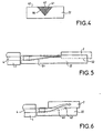
- the engraving 21 is for example filled with a material 41 of refractive index different from the substrate 22 as illustrated in FIG.
- Guiding material 41 is for example a polymer or a silica.
- the guiding material 41 remains in engraving 21.
- the guiding material is demolded.
- the filling must preferably be clean. That is, there is especially no overflow of material, the surface 42 of the material 41 being plane and at the same level as the surface 43 of the substrate 22. Such a clean filling can be easily achieved with the material still to the viscous state, before hardening.
- the guiding material 41 can be a polymer or a silica. More generally, it can be a material that is transparent to optical waves and refractive index greater than the index of the ambient environment in which it is situated.
- a metal layer 44 is for example deposited on the inner surface of the groove or etching 21.
- the metal layer 44 can be replaced by any layer that reflects the light sufficiently.
- a good optical isolation can thus be obtained for example by means of a silicon oxide layer or silicon nitride layer.
- silicon oxide constitutes a good material of confinement. he is indeed interesting because its growth by oxidation is an operation classic microelectronics.
- the substrate being silicon for example
- the internal surface of the etching is oxidized and it forms naturally a layer of silicon oxide.
- Layer 44 can obviously be deposited by any other means, in particular in the form of thin film. In case of demolding, this layer can be demolded with the central material 41. In a particular embodiment, it is then possible to cover the opening of the groove 21 with a metal layer, the light can then be guided in a vacuum between layers metal, without the use of a guiding material.
- FIG. 5 illustrates, by a longitudinal sectional view, a mode possible embodiment of a coupling device according to the invention.
- This one provides the coupling between an optical fiber 1 and a component Optoelectronics 2.
- the coupling device includes a waveguide optical 51 having the shape of a funnel.
- This guide is made by engraving on a crystalline substrate 22.
- the interior of the engraving is covered with a metal layer.
- the heart 4 of the fiber is placed facing the large section of the guide 51. As illustrated by the Figures 3a to 3c, the guide section decreases to a final section. This last is placed next to the optoelectronic component 2, plus particularly of the optical waveguide internal to this component 2.
- the substrate 22 comprises a reception range 52 adapted component 2.
- This range is in particular dug into the substrate of so that the input of the component guide is positioned as well as perfectly as possible in front of the output of the coupling guide 51.
- the crystalline substrate and the optoelectronic component can be made from the same crystalline lens, for example from a same silicon element.
- the positioning of the guide coupling 51, that is to say in fact of the preferential etching, with respect to internal guide to the component is relatively easy since this positioning is obtained by construction. It does not remain then, in practical, than to position the heart of the fiber opposite the entrance of the coupling guide 51, which is all the easier as the latter comprises a section of the same order of magnitude as the heart, or even higher.
- FIG. 6 presents another possible embodiment of a coupling device according to the invention.
- This embodiment differs from preceded by the fact that the optical waveguide 61 of the device of coupling, always in the form of a three-dimensional funnel, ends with a section, or depth, substantially zero.
- the heart 4 of the optical fiber is always placed opposite the large section of the coupling guide 61, but the optoelectronic component is located above this guide, plus particularly above its termination 62.
- the guided optical wave is then propagates in the optoelectronic component by evanescence by the upper opening of the guide 61, the one that is in contact with the component optoelectronics.
- FIGS. 7a and 7b illustrate, by a sectional view, another exemplary embodiment of a coupling device according to the invention. More particularly, this device comprises a guide obtained by etching according to the invention which indirectly guides the luminous flux between the two components to be coupled.
- the wave optical is directly guided in the space defined by the interior of the In FIGS. 7a and 7b, the light 73 is not guided to the interior of the engraving or space 71 defined by it but in a ribbon 72 optical guide still called "rib waveguide" in the literature Anglo-Saxon.
- the optical guide 72 that is to say the material of heart, is a layer deposited above the filling material 41 of engraving.
- the filling material 41 overflows, for example engraving.
- the part of material inside the engraving plays then a role of potential well illustrated by the evolution of the light section guided between Figure 7a and Figure 7b.
- the groove has a funnel shape to three dimensions. Between Figure 7a and Figure 7b, the depth of the guide indirect 71 has evolved, the depth being greater in Figure 7b. These two figures show that the deeper the engraving, or the guide indirect, is important plus the light section 73 guided shrinks. The funnel function of the guided light flow is then ensured.
- the filling material can be demolded, after hardening.
- the invention can be applied in many areas. It can thus be applied in the field of optically high-speed digital telecommunications, for the computer routing, for reconfigurable microwave systems, for the synthesis of delays and the formation of beams in the antennas at electronic scanning, for optical interconnections of processors numerically or for computer interconnections. More generally, the invention applies in systems where it is necessary to couple optical components, including optical fibers, with components e.
- the method according to the invention could be applied to the production of guides which are not intended to convey luminous flux, but for example flows of matter.
- the invention could thus apply for the realization of fluid guides in microsystems, where it is necessary in particular to control the width but also the depth of guides.
- the fluids are channeled by etching 21.
Landscapes
- Physics & Mathematics (AREA)
- Engineering & Computer Science (AREA)
- Microelectronics & Electronic Packaging (AREA)
- General Physics & Mathematics (AREA)
- Optics & Photonics (AREA)
- Power Engineering (AREA)
- Optical Couplings Of Light Guides (AREA)
- Optical Integrated Circuits (AREA)
Description
- d'une part les composants optoélectroniques, tels que par exemple les lasers, les diodes laser, les modulateurs électro-optiques, les photodiodes ou les amplificateurs optiques ;
- d'autre part les fibres optiques.
- la figure 1, une représentation schématique d'un couplage optique entre une fibre optique et un composant optoélectronique ;
- la figure 2, un principe de réalisation d'un guide selon l'invention par une gravure préférentielle dans un matériau cristallin ;
- les figures 3a, 3b et 3c, un exemple de gravure permettant d'obtenir un guide en forme d'entonnoir ;
- la figure 4, une étape possible du procédé selon l'invention comportant une phase de remplissage de la gravure par un matériau d'indice de réfraction adéquate ;
- les figures 5 et 6, des exemples de réalisation d'un dispositif de couplage optique entre deux composants comportant un guide selon l'invention ;
- les figures 7a et 7b, un exemple de réalisation d'un dispositif de couplage optique comportant un guide selon l'invention effectuant un guidage par arête du flux lumineux entre les deux composants.
Claims (18)
- Procédé de réalisation d'un guide d'onde optique, caractérisé en ce qu'il comporte :une étape de gravure (21) dans un substrat (22) à structure cristalline, la gravure étant effectuée suivant une direction privilégiée de la structure cristalline de sorte que la profondeur de la gravure varie avec la largeur de la gravure,une étape de remplissage de la gravure ainsi formée par un matériau d'indice de réfraction supérieur à l'indice de réfraction du substrat (22).
- Procédé selon la revendication 1, caractérisé en ce que la largeur de la gravure varie pour former un entonnoir à trois dimensions.
- Procédé selon l'une quelconque des revendications 1 ou 2, caractérisé en ce que le matériau de remplissage (41) est un polymère.
- Procédé selon l'une quelconque des revendications 1 ou 2, caractérisé en ce que le matériau de remplissage (41) est une silice.
- Procédé selon l'une quelconque des revendications précédentes, caractérisé en ce qu'une couche d'isolant optique (44) est déposée sur la surface intérieure de la gravure (21).
- Procédé selon la revendication 5, caractérisé en ce que la couche (44) est une couche métallique.
- Procédé selon la revendication 5, caractérisé en ce que la couche (44) est une couche d'oxyde de silicium.
- Procédé selon la revendication 5, caractérisé en ce que la couche (44) est une couche de nitrure de silicium.
- Procédé selon l'une quelconque des revendications précédentes, caractérisé en ce qu'après durcissement, le matériau de remplissage (41) est démoulé de la gravure (21).
- Dispositif de couplage optique entre deux composants (1, 2), caractérisé en ce qu'il comporte un guide d'onde optique entre les deux composants, le guide d'onde optique étant obtenu selon l'une quelconque des revendications précédentes.
- Dispositif selon la revendication 10, caractérisé en ce que le guide (51) ayant la forme d'un entonnoir à trois dimensions, sa section décroít jusqu'à une section non nulle.
- Dispositif selon la revendication 11, caractérisé en ce qu'une plage est creusée dans le substrat (22) pour accueillir un composant optoélectronique (2), le guide d'onde optique de ce dernier coïncidant avec le guide (51) du dispositif.
- Dispositif selon la revendication 12 caractérisé en ce que le composant optoélectronique (2) est réalisé dans le même élément cristallin que le substrat (22).
- Dispositif selon la revendication 12, caractérisé en ce que le guide (61) ayant la forme d'un entonnoir à trois dimensions, sa section décroít jusqu'à une section nulle.
- Dispositif selon la revendication 10, caractérisé en ce qu'il comporte un guide optique à ruban (72) déposé sur un matériau (41) de remplissage de la gravure (21), l'onde optique transitant à l'intérieur de ce guide à ruban (72).
- Dispositif selon l'une quelconque des revendications 10 à 15, caractérisé en ce que le substrat (22) est en silicium.
- Dispositif selon l'une quelconque des revendications 10 à 15, caractérisé en ce que le substrat (22) est en arséniure de gallium.
- Dispositif selon l'une quelconque des revendications 10 à 15, caractérisé en ce que le substrat (22) est en phosphure d'indium.
Applications Claiming Priority (2)
| Application Number | Priority Date | Filing Date | Title |
|---|---|---|---|
| FR0013848A FR2816064B1 (fr) | 2000-10-27 | 2000-10-27 | Procede de realisation d'un guide d'onde, notamment optique, et dispositif de couplage optique comportant un tel guide |
| FR0013848 | 2000-10-27 |
Publications (3)
| Publication Number | Publication Date |
|---|---|
| EP1202085A2 EP1202085A2 (fr) | 2002-05-02 |
| EP1202085A3 EP1202085A3 (fr) | 2002-10-30 |
| EP1202085B1 true EP1202085B1 (fr) | 2005-12-21 |
Family
ID=8855836
Family Applications (1)
| Application Number | Title | Priority Date | Filing Date |
|---|---|---|---|
| EP20010402721 Expired - Lifetime EP1202085B1 (fr) | 2000-10-27 | 2001-10-19 | Procédé de réalisation d'un guide d'onde, notamment optique, et dispositif de couplage optique comportant un tel guide |
Country Status (3)
| Country | Link |
|---|---|
| EP (1) | EP1202085B1 (fr) |
| DE (1) | DE60116032D1 (fr) |
| FR (1) | FR2816064B1 (fr) |
Cited By (1)
| Publication number | Priority date | Publication date | Assignee | Title |
|---|---|---|---|---|
| US8064741B2 (en) | 2003-12-29 | 2011-11-22 | Mosaid Technologies Incorporated | Optical coupling device |
Family Cites Families (8)
| Publication number | Priority date | Publication date | Assignee | Title |
|---|---|---|---|---|
| US4520485A (en) * | 1981-03-17 | 1985-05-28 | Matsushita Electric Industrial Co., Ltd. | Semiconductor device |
| US4946239A (en) * | 1988-09-27 | 1990-08-07 | Georgia Tech Research Corporation | Optical power isolator |
| US5402511A (en) * | 1993-06-11 | 1995-03-28 | The United States Of America As Represented By The Secretary Of The Army | Method of forming an improved tapered waveguide by selectively irradiating a viscous adhesive resin prepolymer with ultra-violet light |
| US5473710A (en) * | 1993-10-08 | 1995-12-05 | Industrial Technology Research Institute | Controlled tapered angle etching process for fabricating optical integrated circuits |
| US5439782A (en) * | 1993-12-13 | 1995-08-08 | At&T Corp. | Methods for making microstructures |
| FR2719388B1 (fr) * | 1994-05-02 | 1996-07-19 | Frederic Ghirardi | Dispositif semi-conducteur optoélectronique comportant un adaptateur de mode intégré. |
| DE19626113A1 (de) * | 1996-06-28 | 1998-01-02 | Sel Alcatel Ag | Optisches Halbleiterbauelement mit tiefem Rippenwellenleiter |
| US6118915A (en) * | 1997-06-30 | 2000-09-12 | Kyocera Corporation | Hybrid assembly of bulk optical elements and method of making the same |
-
2000
- 2000-10-27 FR FR0013848A patent/FR2816064B1/fr not_active Expired - Fee Related
-
2001
- 2001-10-19 EP EP20010402721 patent/EP1202085B1/fr not_active Expired - Lifetime
- 2001-10-19 DE DE2001616032 patent/DE60116032D1/de not_active Expired - Lifetime
Cited By (1)
| Publication number | Priority date | Publication date | Assignee | Title |
|---|---|---|---|---|
| US8064741B2 (en) | 2003-12-29 | 2011-11-22 | Mosaid Technologies Incorporated | Optical coupling device |
Also Published As
| Publication number | Publication date |
|---|---|
| EP1202085A2 (fr) | 2002-05-02 |
| FR2816064B1 (fr) | 2003-03-07 |
| FR2816064A1 (fr) | 2002-05-03 |
| DE60116032D1 (de) | 2006-01-26 |
| EP1202085A3 (fr) | 2002-10-30 |
Similar Documents
| Publication | Publication Date | Title |
|---|---|---|
| EP0637764B1 (fr) | Procédé de fabrication d'une structure de couplage optique intégrante un guide optique clivé à un support de fibre optique | |
| EP3287822B1 (fr) | Circuit photonique comportant une structure de couplage à un dispositif extérieur | |
| FR3066615B1 (fr) | Puce photonique a structure de collimation integree | |
| EP2169436A1 (fr) | Coupleur de lumière entre une fibre optique et un guide d'onde réalisé sur un substrat SOI | |
| EP0451047B1 (fr) | Composant optique intégré protégé contre l'environnement et son procédé de fabrication | |
| EP2515096B1 (fr) | Détecteur de gaz photoacoustique à cellule de Helmholtz | |
| EP0539298B1 (fr) | Modulateur électrooptique intégré et procédé de fabrication de ce modulateur | |
| EP3404457A1 (fr) | Puce photonique à structure réfléchissante de repliement de trajet optique | |
| FR3069070A1 (fr) | Dispositif de focalisation optique a pseudo-gradient d'indice | |
| FR2570839A1 (fr) | Dispositif de couplage entre des guides d'onde, monolithiquement integre avec ceux-ci sur un substrat semiconducteur | |
| EP3994509B1 (fr) | Assemblage d'un composant semi-conducteur actif et d'un composant optique passif à base de silicium | |
| EP2267500A2 (fr) | Structure et procédé d'alignement d'une fibre optique et d'un guide d'ondes submicronique | |
| EP2216663B1 (fr) | Structure et procédé d'alignement d'une fibre optique et d'un guide d'ondes submicronique | |
| FR2719388A1 (fr) | Dispositif semi-conducteur optoélectronique comportant un adaptateur de mode intégré. | |
| EP2141520A1 (fr) | Dispositif de couplage à birefringence compensée | |
| EP0665450B1 (fr) | Dispositif de transition de guide optique et procédé de sa réalisation | |
| EP2442164A1 (fr) | Duplexeur optique nanophotonique | |
| EP1190270B1 (fr) | Connexion optique pour circuit electronique integre et application aux interconnexions de tels circuits | |
| EP1202085A2 (fr) | Procédé de réalisation d'un guide d'onde, notamment optique, et dispositif de couplage optique comportant un tel guide | |
| FR2501383A1 (fr) | Coupleur directif et selectif | |
| EP0234990A1 (fr) | Procédé et appareillage pour positionner et immobiliser une terminaison de fibre optique dans un embout de connexion,embout de connexion et connecteur optique ainsi réalisés | |
| WO2022180039A1 (fr) | Emetteur optoelectronique a antenne reseau a commande de phase comportant une source laser evasee | |
| EP4441559B1 (fr) | Emetteur optoelectronique a antenne reseau a commande de phase comportant des antennes optiques adaptees a emettre un rayonnement lumineux selon un profil d'emission et une direction predefinis | |
| EP0187581A1 (fr) | Diodes émettrices/réceptrices de lumière, et éléments de transmission optiques non réciproques, intégrés, et leur procédé de fabrication | |
| FR2840415A1 (fr) | Procede de realisation de microguides optiques a tres faibles pertes |
Legal Events
| Date | Code | Title | Description |
|---|---|---|---|
| PUAI | Public reference made under article 153(3) epc to a published international application that has entered the european phase |
Free format text: ORIGINAL CODE: 0009012 |
|
| AK | Designated contracting states |
Kind code of ref document: A2 Designated state(s): AT BE CH CY DE DK ES FI FR GB GR IE IT LI LU MC NL PT SE TR |
|
| AX | Request for extension of the european patent |
Free format text: AL;LT;LV;MK;RO;SI |
|
| PUAL | Search report despatched |
Free format text: ORIGINAL CODE: 0009013 |
|
| AK | Designated contracting states |
Kind code of ref document: A3 Designated state(s): AT BE CH CY DE DK ES FI FR GB GR IE IT LI LU MC NL PT SE TR |
|
| AX | Request for extension of the european patent |
Free format text: AL;LT;LV;MK;RO;SI |
|
| RIC1 | Information provided on ipc code assigned before grant |
Free format text: 7G 02B 6/12 A |
|
| 17P | Request for examination filed |
Effective date: 20030422 |
|
| 17Q | First examination report despatched |
Effective date: 20030528 |
|
| AKX | Designation fees paid |
Designated state(s): BE DE FR GB IT NL |
|
| GRAP | Despatch of communication of intention to grant a patent |
Free format text: ORIGINAL CODE: EPIDOSNIGR1 |
|
| GRAS | Grant fee paid |
Free format text: ORIGINAL CODE: EPIDOSNIGR3 |
|
| GRAA | (expected) grant |
Free format text: ORIGINAL CODE: 0009210 |
|
| AK | Designated contracting states |
Kind code of ref document: B1 Designated state(s): BE DE FR GB IT NL |
|
| PG25 | Lapsed in a contracting state [announced via postgrant information from national office to epo] |
Ref country code: IT Free format text: LAPSE BECAUSE OF FAILURE TO SUBMIT A TRANSLATION OF THE DESCRIPTION OR TO PAY THE FEE WITHIN THE PRESCRIBED TIME-LIMIT;WARNING: LAPSES OF ITALIAN PATENTS WITH EFFECTIVE DATE BEFORE 2007 MAY HAVE OCCURRED AT ANY TIME BEFORE 2007. THE CORRECT EFFECTIVE DATE MAY BE DIFFERENT FROM THE ONE RECORDED. Effective date: 20051221 Ref country code: NL Free format text: LAPSE BECAUSE OF FAILURE TO SUBMIT A TRANSLATION OF THE DESCRIPTION OR TO PAY THE FEE WITHIN THE PRESCRIBED TIME-LIMIT Effective date: 20051221 |
|
| REG | Reference to a national code |
Ref country code: GB Ref legal event code: FG4D Free format text: NOT ENGLISH |
|
| REF | Corresponds to: |
Ref document number: 60116032 Country of ref document: DE Date of ref document: 20060126 Kind code of ref document: P |
|
| PG25 | Lapsed in a contracting state [announced via postgrant information from national office to epo] |
Ref country code: DE Free format text: LAPSE BECAUSE OF FAILURE TO SUBMIT A TRANSLATION OF THE DESCRIPTION OR TO PAY THE FEE WITHIN THE PRESCRIBED TIME-LIMIT Effective date: 20060322 |
|
| GBT | Gb: translation of ep patent filed (gb section 77(6)(a)/1977) |
Effective date: 20060306 |
|
| NLV1 | Nl: lapsed or annulled due to failure to fulfill the requirements of art. 29p and 29m of the patents act | ||
| PLBE | No opposition filed within time limit |
Free format text: ORIGINAL CODE: 0009261 |
|
| STAA | Information on the status of an ep patent application or granted ep patent |
Free format text: STATUS: NO OPPOSITION FILED WITHIN TIME LIMIT |
|
| 26N | No opposition filed |
Effective date: 20060922 |
|
| BERE | Be: lapsed |
Owner name: *THALES Effective date: 20061031 |
|
| PG25 | Lapsed in a contracting state [announced via postgrant information from national office to epo] |
Ref country code: BE Free format text: LAPSE BECAUSE OF FAILURE TO SUBMIT A TRANSLATION OF THE DESCRIPTION OR TO PAY THE FEE WITHIN THE PRESCRIBED TIME-LIMIT Effective date: 20061031 |
|
| PGFP | Annual fee paid to national office [announced via postgrant information from national office to epo] |
Ref country code: FR Payment date: 20121018 Year of fee payment: 12 |
|
| PGFP | Annual fee paid to national office [announced via postgrant information from national office to epo] |
Ref country code: GB Payment date: 20121017 Year of fee payment: 12 Ref country code: IT Payment date: 20121012 Year of fee payment: 12 |
|
| GBPC | Gb: european patent ceased through non-payment of renewal fee |
Effective date: 20131019 |
|
| PG25 | Lapsed in a contracting state [announced via postgrant information from national office to epo] |
Ref country code: GB Free format text: LAPSE BECAUSE OF NON-PAYMENT OF DUE FEES Effective date: 20131019 |
|
| REG | Reference to a national code |
Ref country code: FR Ref legal event code: ST Effective date: 20140630 |
|
| PG25 | Lapsed in a contracting state [announced via postgrant information from national office to epo] |
Ref country code: IT Free format text: LAPSE BECAUSE OF NON-PAYMENT OF DUE FEES Effective date: 20131019 Ref country code: FR Free format text: LAPSE BECAUSE OF NON-PAYMENT OF DUE FEES Effective date: 20131031 |