EP1200341B1 - Patterned carbon nanotube films - Google Patents
Patterned carbon nanotube films Download PDFInfo
- Publication number
- EP1200341B1 EP1200341B1 EP00926580A EP00926580A EP1200341B1 EP 1200341 B1 EP1200341 B1 EP 1200341B1 EP 00926580 A EP00926580 A EP 00926580A EP 00926580 A EP00926580 A EP 00926580A EP 1200341 B1 EP1200341 B1 EP 1200341B1
- Authority
- EP
- European Patent Office
- Prior art keywords
- process according
- substrate
- group
- photoresist
- metal
- Prior art date
- Legal status (The legal status is an assumption and is not a legal conclusion. Google has not performed a legal analysis and makes no representation as to the accuracy of the status listed.)
- Expired - Lifetime
Links
Images


Classifications
-
- G—PHYSICS
- G03—PHOTOGRAPHY; CINEMATOGRAPHY; ANALOGOUS TECHNIQUES USING WAVES OTHER THAN OPTICAL WAVES; ELECTROGRAPHY; HOLOGRAPHY
- G03F—PHOTOMECHANICAL PRODUCTION OF TEXTURED OR PATTERNED SURFACES, e.g. FOR PRINTING, FOR PROCESSING OF SEMICONDUCTOR DEVICES; MATERIALS THEREFOR; ORIGINALS THEREFOR; APPARATUS SPECIALLY ADAPTED THEREFOR
- G03F7/00—Photomechanical, e.g. photolithographic, production of textured or patterned surfaces, e.g. printing surfaces; Materials therefor, e.g. comprising photoresists; Apparatus specially adapted therefor
- G03F7/26—Processing photosensitive materials; Apparatus therefor
- G03F7/40—Treatment after imagewise removal, e.g. baking
-
- B—PERFORMING OPERATIONS; TRANSPORTING
- B82—NANOTECHNOLOGY
- B82Y—SPECIFIC USES OR APPLICATIONS OF NANOSTRUCTURES; MEASUREMENT OR ANALYSIS OF NANOSTRUCTURES; MANUFACTURE OR TREATMENT OF NANOSTRUCTURES
- B82Y30/00—Nanotechnology for materials or surface science, e.g. nanocomposites
-
- B—PERFORMING OPERATIONS; TRANSPORTING
- B82—NANOTECHNOLOGY
- B82Y—SPECIFIC USES OR APPLICATIONS OF NANOSTRUCTURES; MEASUREMENT OR ANALYSIS OF NANOSTRUCTURES; MANUFACTURE OR TREATMENT OF NANOSTRUCTURES
- B82Y40/00—Manufacture or treatment of nanostructures
-
- C—CHEMISTRY; METALLURGY
- C01—INORGANIC CHEMISTRY
- C01B—NON-METALLIC ELEMENTS; COMPOUNDS THEREOF; METALLOIDS OR COMPOUNDS THEREOF NOT COVERED BY SUBCLASS C01C
- C01B32/00—Carbon; Compounds thereof
- C01B32/15—Nano-sized carbon materials
- C01B32/158—Carbon nanotubes
- C01B32/16—Preparation
- C01B32/162—Preparation characterised by catalysts
-
- D—TEXTILES; PAPER
- D01—NATURAL OR MAN-MADE THREADS OR FIBRES; SPINNING
- D01F—CHEMICAL FEATURES IN THE MANUFACTURE OF ARTIFICIAL FILAMENTS, THREADS, FIBRES, BRISTLES OR RIBBONS; APPARATUS SPECIALLY ADAPTED FOR THE MANUFACTURE OF CARBON FILAMENTS
- D01F9/00—Artificial filaments or the like of other substances; Manufacture thereof; Apparatus specially adapted for the manufacture of carbon filaments
- D01F9/08—Artificial filaments or the like of other substances; Manufacture thereof; Apparatus specially adapted for the manufacture of carbon filaments of inorganic material
- D01F9/12—Carbon filaments; Apparatus specially adapted for the manufacture thereof
- D01F9/127—Carbon filaments; Apparatus specially adapted for the manufacture thereof by thermal decomposition of hydrocarbon gases or vapours or other carbon-containing compounds in the form of gas or vapour, e.g. carbon monoxide, alcohols
-
- B—PERFORMING OPERATIONS; TRANSPORTING
- B82—NANOTECHNOLOGY
- B82Y—SPECIFIC USES OR APPLICATIONS OF NANOSTRUCTURES; MEASUREMENT OR ANALYSIS OF NANOSTRUCTURES; MANUFACTURE OR TREATMENT OF NANOSTRUCTURES
- B82Y10/00—Nanotechnology for information processing, storage or transmission, e.g. quantum computing or single electron logic
-
- C—CHEMISTRY; METALLURGY
- C01—INORGANIC CHEMISTRY
- C01B—NON-METALLIC ELEMENTS; COMPOUNDS THEREOF; METALLOIDS OR COMPOUNDS THEREOF NOT COVERED BY SUBCLASS C01C
- C01B2202/00—Structure or properties of carbon nanotubes
- C01B2202/08—Aligned nanotubes
-
- H—ELECTRICITY
- H01—ELECTRIC ELEMENTS
- H01J—ELECTRIC DISCHARGE TUBES OR DISCHARGE LAMPS
- H01J2201/00—Electrodes common to discharge tubes
- H01J2201/30—Cold cathodes
- H01J2201/304—Field emission cathodes
- H01J2201/30446—Field emission cathodes characterised by the emitter material
- H01J2201/30453—Carbon types
- H01J2201/30469—Carbon nanotubes (CNTs)
-
- Y—GENERAL TAGGING OF NEW TECHNOLOGICAL DEVELOPMENTS; GENERAL TAGGING OF CROSS-SECTIONAL TECHNOLOGIES SPANNING OVER SEVERAL SECTIONS OF THE IPC; TECHNICAL SUBJECTS COVERED BY FORMER USPC CROSS-REFERENCE ART COLLECTIONS [XRACs] AND DIGESTS
- Y10—TECHNICAL SUBJECTS COVERED BY FORMER USPC
- Y10S—TECHNICAL SUBJECTS COVERED BY FORMER USPC CROSS-REFERENCE ART COLLECTIONS [XRACs] AND DIGESTS
- Y10S977/00—Nanotechnology
- Y10S977/84—Manufacture, treatment, or detection of nanostructure
- Y10S977/842—Manufacture, treatment, or detection of nanostructure for carbon nanotubes or fullerenes
- Y10S977/843—Gas phase catalytic growth, i.e. chemical vapor deposition
-
- Y—GENERAL TAGGING OF NEW TECHNOLOGICAL DEVELOPMENTS; GENERAL TAGGING OF CROSS-SECTIONAL TECHNOLOGIES SPANNING OVER SEVERAL SECTIONS OF THE IPC; TECHNICAL SUBJECTS COVERED BY FORMER USPC CROSS-REFERENCE ART COLLECTIONS [XRACs] AND DIGESTS
- Y10—TECHNICAL SUBJECTS COVERED BY FORMER USPC
- Y10S—TECHNICAL SUBJECTS COVERED BY FORMER USPC CROSS-REFERENCE ART COLLECTIONS [XRACs] AND DIGESTS
- Y10S977/00—Nanotechnology
- Y10S977/84—Manufacture, treatment, or detection of nanostructure
- Y10S977/887—Nanoimprint lithography, i.e. nanostamp
-
- Y—GENERAL TAGGING OF NEW TECHNOLOGICAL DEVELOPMENTS; GENERAL TAGGING OF CROSS-SECTIONAL TECHNOLOGIES SPANNING OVER SEVERAL SECTIONS OF THE IPC; TECHNICAL SUBJECTS COVERED BY FORMER USPC CROSS-REFERENCE ART COLLECTIONS [XRACs] AND DIGESTS
- Y10—TECHNICAL SUBJECTS COVERED BY FORMER USPC
- Y10S—TECHNICAL SUBJECTS COVERED BY FORMER USPC CROSS-REFERENCE ART COLLECTIONS [XRACs] AND DIGESTS
- Y10S977/00—Nanotechnology
- Y10S977/84—Manufacture, treatment, or detection of nanostructure
- Y10S977/895—Manufacture, treatment, or detection of nanostructure having step or means utilizing chemical property
- Y10S977/896—Chemical synthesis, e.g. chemical bonding or breaking
Definitions
- This invention relates to carbon nanotube materials and processes for their preparation.
- the invention relates to patterned aligned carbon nanotube films and to processes for their preparation which involve the use of photoresist materials.
- the invention also relates to the construction of devices from such materials for practical applications in many areas including as electron field emitters, artificial actuators, chemical sensors, gas storages, molecular-filtration membranes, energy-absorbing materials, molecular transistors and other optoelectronic devices.
- Carbon nanotubes usually have a diameter in the order of tens of angstroms and the length of up to several micrometers. These elongated nanotubes consist of carbon hexagons arranged in a concentric manner with both ends of the tubes normally capped by pentagon-containing, fullerene-like structures. They can behave as a semiconductor or metal depending on their diameter and helicity of the arrangement of graphitic rings in the walls, and dissimilar carbon nanotubes may be joined together allowing the formation of molecular wires with interesting electrical, magnetic, nonlinear optical, thermal and mechanical properties. These unusual properties have led to diverse potential applications for carbon nanotubes in material science and nanotechnology.
- carbon nanotubes have been proposed as new materials for electron field emitters in panel displays, single-molecular transistors, scanning probe microscope tips, gas and electrochemical energy storages, catalyst and proteins/DNA supports, molecular-filtration membranes, and energy-absorbing materials (see, for example: M. Dresselhaus, et al., Phys. World, January, 33, 1998 ; P.M. Ajayan, and T.W. Ebbesen, Rep. Prog. Phys., 60, 1027, 1997 ; R. Dagani, C&E News, January 11, 31, 1999 ).
- Carbon nanotubes synthesised by most of the common techniques, such as arc discharge ( Iijima, S. Nature 354, 56-58, 1991 ; Ebbesen, T. W. & Aegean, P.M. Nature 358, 220-222, 1992 ) and catalytic pyrolysis (See, for example: End. M et al. J. Pays. Chum. Solids 54, 1841-1848, 1994 ; Ivanov. V. et al., Chum. Pays. Let.
- arc discharge Iijima, S. Nature 354, 56-58, 1991 ; Ebbesen, T. W. & Aegean, P.M. Nature 358, 220-222, 1992
- catalytic pyrolysis See, for example: End. M et al. J. Pays. Chum. Solids 54, 1841-1848, 1994 ; Ivanov. V. et al., Chum. Pays. Let.
- aligned carbon nanotubes have recently been prepared either by post-synthesis manipulation (see, for example: Aegean, P. M., et al., Science 265, 1212-1214, 1994 ; De Heer, W.A. et al. Science 268, 845-847, 1995 ) or by synthesis-induced alignment (see, for example: W. Z. Li, Science, 274, 1701, 1996 ; Che, G., Nature, 393, 346, 1998 ; Z. G. Ren, et al., Science, 282,1105, 1998 ; C. N., Rao, et al., J.C.S., Chem. Commun., 1525, 1998 ).
- the present invention provides a process for preparing a patterned layer of aligned carbon nanotubes on a substrate including:
- this photolithographic patterning method together with a novel contact printing transfer technique, allows the pattern formation of aligned carbon nanotubes on various substrates at a micrometer/submicrometer resolution.
- the technique provides a route to patterned formations of aligned carbon nanotubes which have not been achievable according to methods described in the prior art.
- the process according to the present invention is easy to perform and provides a convenient route to patterned aligned carbon nanotubes with controllable geometries.
- photoresist is used herein in its broadest sense to refer to any organic material capable of polymerising or otherwise transforming upon exposure to electromagnetic radiation such that, upon exposure, its solubility characteristics are changed relative to unexposed material.
- photoresponsive materials include, but are not limited to, diazonaphthoquinone (DNQ)-based photoresists, such as cresol novolac resin (from Shipley), Ozatec PK 14 (from Hoechst), as well as other possible polymers including, inter alia, epoxy resins, polyanilines, polymethyl methacrylate, polystyrenes, and polydienes.
- DNQ diazonaphthoquinone
- cresol novolac resin from Shipley
- Ozatec PK 14 from Hoechst
- other possible polymers including, inter alia, epoxy resins, polyanilines, polymethyl methacrylate, polystyrenes, and polydienes.
- the base insoluble resin is transformed into a base soluble entity following exposure to light.
- the substrate to which the photoresist layer is applied can be any substrate which is capable of withstanding the pyrolysis or CVD (chemical vapour deposition) conditions employed, for nanotube growth and which is capable of supporting aligned carbon nanotube growth.
- suitable substrates include all types of glass that provide sufficient thermal stability according to the synthesis temperature applied, such as quartz glass, as well as alumina, graphite, mica, mesaporous silica, silicon water, nanoporous alumina or ceramic plates.
- the substrate is glass, in particular, quartz glass or silicon water.
- the substrate may also include a coating of a material which is capable of supporting carbon nanotube growth under the conditions employed.
- the coating may be of any metal, metaloxide, metal alloy or compound thereof, which may have conducting or semiconducting properties.
- suitable metals include Au, Pt, Cu, Cr, Ni, Fe, Co and Pd.
- suitable compounds are metal oxides, metal carbides, metal nitrides, metal sulfides and metal borides.
- suitable metal oxides include indium tin oxide (ITO), Al 2 O 3 , TiO 2 and MgO.
- Examples of semiconducting materials include gallium arsenide, aluminium arsenide, aluminium sulphide and gallium sulphide.
- the patterning of the aligned carbon nanotubes is achieved by creating a region on the substrate which is incapable of supporting nanotube growth.
- the pattern is created on the substrate by applying an appropriate mask to the photoresist layer such that part of the photoresist layer is capable of being exposed to electromagnetic radiation, while the remaining photoresist layer is substantially shielded from such electromagnetic radiation.
- the patterning of the subsequently synthesised aligned carbon nanotube layer will be defined by the positive or negative of the mask.
- One suitable mask is a quartz plate coated with a thin layer of metal micropatterns, where the regions covered by the thin metal layer are opaque while the uncovered areas are transparent to a photo-irradiation beam.
- the photomask may be applied to the photoresist layer by physical pressing.
- the photoresist coated substrate is subjected to electromagnetic radiation to transform the exposed region of the photoresist.
- the transformation which is undergone by the photoresist will depend on the nature and properties of the photoresist. Accordingly the transformation may represent a polymerisation, an oxidation, or other chemical transformation of the photoresist material.
- the transformation should be specific to the exposed region, should result in a change in solubility characteristics relative to the unexposed photoresist, and should be sufficiently permanent to enable selective solubilisation of the exposed or the unexposed photoresist.
- the electromagnetic radiation used to irradiate the exposed photoresist will depend on the nature of the photoresist material used, however for most applications the electromagnetic radiation will be UV radiation.
- the photoresist layer is then developed by contact with a solvent which is capable of dissolving the portion of the photoresist layer which is to later support growth of aligned carbon nanotubes into the desired pattern. This will be either the exposed (transformed) region or the unexposed (untransformed) region.
- the contact with the solvent should be such that the non-dissolved region of the photoresist remains attached to the substrate.
- the nature of the solvent used will depend on the type of photoresist utilised and the nature of the transformation which it undergoes on exposure to electromagnetic radiation.
- cresol novolac resin which is base insoluble
- exposure to UV radiation produces a carboxylic acid moiety which is soluble in base.
- a suitable base such as an alkali metal hydroxide, ammonium hydroxide, tetramethylammonium hydroxide.
- a solvent can be selected which dissolves the unexposed region of the photoresist, such as ethylene glycol, butanediol, dimethyl ether, diethyl ether, methyl ethyl ether, acetone, methyl ethyl ketone.
- polar solvents such as water, ethanol, methanol, acetone and the like on the one hand
- non-polar solvents such as benzene, toluene and the like on the other hand.
- a person skilled in the art would be readily able to select a suitable solvent to dissolve the desired region of the photoresist.
- the next step in the process involves the synthesis of a layer of aligned carbon nanotubes on the region of the substrate from which the photoresist has been dissolved. This may be achieved using a suitable technique for the synthesis of perpendicularly aligned carbon nanotubes.
- the aligned carbon nanotubes are prepared by pyrolysis of a carbon-containing material in the presence of a suitable catalyst for nanotube formation.
- the carbon-containing material may be any compound or substance which includes carbon and which is capable for forming carbon nanotubes when subjected to pyrolysis in the presence of a suitable catalyst.
- suitable carbon-containing materials include alkanes, alkenes, alkynes or aromatic hydrocarbons and their derivatives, for example methane, acetylene, benzene, organometallic compounds of transition metals, for example transition metal phthalocyanines, such as Fe(II) phthalocyanine, and metallocenes such as ferrocene and nickel dicyclopentadiene and evaporable metal complex.
- the catalyst may be any compound, element or substance suitable for catalysing the conversion of a carbon-containing material to aligned carbon nanotubes under pyrolytic conditions.
- the catalyst may be a transition metal, such as Fe, Co, Al, Ni, Mn, Pd, Cr or alloys thereof in any suitable oxidation state.
- the catalyst may be incorporated into the substrate or may be included in the carbon-containing material.
- carbon-containing materials which include a transition metal catalyst are Fe(II) phthalocyanine, Ni(II) phthalocyanine and ferrocene.
- the pyrolysis condition employed will depend on the type of carbon-containing material employed and the type of catalyst, as well as the length and density of the nanotubes required. In this regard it is possible to vary the pyrolysis conditions, such as the temperature, time, pressure or flow rate through the pyrolysis reactor, to obtain nanotubes having different characteristics.
- performing the pyrolysis at a higher temperature may produce nanotubes having different base-end structures relative to those prepared at a lower temperature.
- the pyrolysis will generally be performed with a temperature range of 500°C to 1100°C.
- lowering the flow rate through a flow-type pyrolysis reactor may result in a smaller packing density of the nanotubes and vice versa.
- a person skilled in the art would be able to select and control the conditions of pyrolysis to obtain nanotubes having the desired characteristics.
- the photoresist material remaining on the substrate may be dissociated from the carbon nanotubes. This may be achieved using a solvent capable of dissolving the remaining photoresist layer. Alternatively it is possible to disassociate the carbon nanotubes from the substrate by transferring the patterned carbon nanotube layer to another substrate.
- This other substrate may be another substrate capable of supporting carbon nanotube growth, or may be a metal, metal oxide, semi-conductor material or a polymer.
- suitable polymers include adhesive coated polymers such as cellulose tape, conjugated (conducting) polymers, temperature/pressure responsive polymers, bioactive polymers and engineering resins.
- the patterned layer of aligned carbon nanotubes is transferred to another substrate which is capable of supporting carbon nanotube growth
- it is possible to form a hetero-structured nanotube film by subjecting the nanotube coated substrate to conditions for promoting aligned carbon nanotube growth.
- the conditions of nanotube formation may be controlled or adjusted such that the length of the further nanotubes is different to the length of the nanotubes making up the original patterned layer.
- This second layer of nanotubes will tend to grow in the spaces defined by the original patterned layer. It may also be possible to adjust conditions such that there is some further nanotube growth on top of the original patterned layer.
- the nanotube patterns on quartz plates may also be separated from the substrate, while retaining the integrity of the pattern by immersing the sample in an aqueous hydrofluoric acid solution (10-40% w/w) for an appropriate period.
- the patterned carbon nanotube film may be incorporated into a multilayer structure including layers of other materials, such as metals, metal oxides, semiconductor materials or polymers.
- the patterned carbon nanotube film prepared in accordance with the present invention and the devices including these patterned films represent further aspects of the present invention.
- the patterned film prepared in accordance with any one of the processes of the present invention and devices, materials coated with or including these multilayer films represent further aspects of the present invention.
- the invention allows the preparation of a large variety of patterned films and structures.
- the processes of the present invention and the patterned structures formed may have use in the following applications:
- Aligned carbon nanotubes were prepared by pyrolysis of iron (II) phthalocyanine under Ar/H 2 at 800-1100°C using a quartz plate in a flow reactor consisting of a quartz glass tube and a dual furnace fitted with independent temperature controllers ( Figure 1 ).
- Figure 2a represents a typical scanning electron microscopic (SEM, XL-30 FEG SEM, Philips, at 5 KV) image of the carbon nanotubes, showing that the as-synthesised nanotubes align almost normal to the substrate surface.
- the aligned nanotubes are densely packed with a fairly uniform tubular length of ca. 25 ⁇ m.
- the length of the aligned nanotubes can be varied over a wide range (from a few to several tens of micrometers) in a controllable fashion by changing the experimental conditions (e.g . the pyrolysis time, flow rate).
- a well-graphitised structure with ca. 40 concentric carbon shells and an outer diameter of ca. 40 nm is illustrated in the high resolution transmission electron microscopic HR-TEM, CM30, Philips, at 300 KV) image of an individual nanotube ( Figure 2b ).
- cresol novolac resin was used as a positive photoresist.
- the indene carboxylic acid derivative of the photoresist formed in regions exposed to UV is base soluble while the unexposed photoresist remains to be insoluble under the same conditions.
- the steps involved in forming the pattern are shown schematically in Figure 3 .
- a photoresist solution was prepared by dissolving 30g of naphthoquinone diazid-cresol novolac resin in 100 mL ethoxy ethyl acetate. Spin-casting of the photoresist solution onto a quartz glass plate resulted in the formation of a photoresist coating, which was baked in an oven at 80°C for 10 min.
- the resultant dry photoresist layer (0.2 ⁇ m thick) was then exposed through a photomask to EIMAC, VARIAN R150-8 at a lamp-sample distance of 111cm for 30 sec.
- the photoresist was then developed in a 1% sodium hydroxide solution for 8 sec. After rinsing with distilled water, the photoresist patterned quartz plate was further baked at 80°C for 10 min.
- the photoresist prepatterned quartz plate prepared in Example 2 was used for growing the aligned nanotubes in accordance with the process described in Example 1.
- the aligned nanotube pattern thus prepared is shown in Figure 4 , the nanotube pattern showing a close replication of the photomask structure.
- aligned nanotube bundles at a submicrometer scale are clearly evident.
Landscapes
- Chemical & Material Sciences (AREA)
- Engineering & Computer Science (AREA)
- Nanotechnology (AREA)
- Physics & Mathematics (AREA)
- Materials Engineering (AREA)
- General Physics & Mathematics (AREA)
- Condensed Matter Physics & Semiconductors (AREA)
- Organic Chemistry (AREA)
- Chemical Kinetics & Catalysis (AREA)
- Crystallography & Structural Chemistry (AREA)
- Inorganic Chemistry (AREA)
- Manufacturing & Machinery (AREA)
- Composite Materials (AREA)
- Thermal Sciences (AREA)
- General Chemical & Material Sciences (AREA)
- Textile Engineering (AREA)
- Carbon And Carbon Compounds (AREA)
Abstract
Description
- This invention relates to carbon nanotube materials and processes for their preparation. In particular the invention relates to patterned aligned carbon nanotube films and to processes for their preparation which involve the use of photoresist materials. The invention also relates to the construction of devices from such materials for practical applications in many areas including as electron field emitters, artificial actuators, chemical sensors, gas storages, molecular-filtration membranes, energy-absorbing materials, molecular transistors and other optoelectronic devices.
- Carbon nanotubes usually have a diameter in the order of tens of angstroms and the length of up to several micrometers. These elongated nanotubes consist of carbon hexagons arranged in a concentric manner with both ends of the tubes normally capped by pentagon-containing, fullerene-like structures. They can behave as a semiconductor or metal depending on their diameter and helicity of the arrangement of graphitic rings in the walls, and dissimilar carbon nanotubes may be joined together allowing the formation of molecular wires with interesting electrical, magnetic, nonlinear optical, thermal and mechanical properties. These unusual properties have led to diverse potential applications for carbon nanotubes in material science and nanotechnology. Indeed, carbon nanotubes have been proposed as new materials for electron field emitters in panel displays, single-molecular transistors, scanning probe microscope tips, gas and electrochemical energy storages, catalyst and proteins/DNA supports, molecular-filtration membranes, and energy-absorbing materials (see, for example: M. Dresselhaus, et al., Phys. World, January, 33, 1998; P.M. Ajayan, and T.W. Ebbesen, Rep. Prog. Phys., 60, 1027, 1997; R. Dagani, C&E News, January 11, 31, 1999).
- For most of the above applications, it is highly desirable to prepare aligned carbon nanotubes so that the properties of individual nanotubes can be easily assessed and they can be incorporated effectively into devices. Carbon nanotubes synthesised by most of the common techniques, such as arc discharge (Iijima, S. Nature 354, 56-58, 1991; Ebbesen, T. W. & Aegean, P.M. Nature 358, 220-222, 1992) and catalytic pyrolysis (See, for example: End. M et al. J. Pays. Chum. Solids 54, 1841-1848, 1994; Ivanov. V. et al., Chum. Pays. Let. 223, 329-335, 1994), often exist in a randomly entangled state (See, for example: T.W. Ebbesen and P.M. Ajayan, Nature 358, 220, 1992. However, aligned carbon nanotubes have recently been prepared either by post-synthesis manipulation (see, for example: Aegean, P. M., et al., Science 265, 1212-1214, 1994; De Heer, W.A. et al. Science 268, 845-847, 1995) or by synthesis-induced alignment (see, for example: W. Z. Li, Science, 274, 1701, 1996; Che, G., Nature, 393, 346, 1998; Z. G. Ren, et al., Science, 282,1105, 1998; C. N., Rao, et al., J.C.S., Chem. Commun., 1525, 1998).
- The number of techniques which have been reported for the pattern formation of aligned carbon nanotubes is very limited (S. Fan, M.G. Chapline, N.R. Franklin, T.W. Tombler, A.M. Cassell, and H. Dai, Science, 283, 512,1999; S. Huang, L. Dai, and A.W.H. Mau, J. Phys, Chem., 103 issue 21, 4223-4227), and the achievable resolutions of the nanotube patterns was, at the best, at several micrometer scale in these cases.
- It has now been found that pattern formation of perpendicularly aligned carbon nanotubes with resolutions up to a sub-micrometer scale can be achieved using a novel photolithographic technique.
- According to a first aspect, the present invention provides a process for preparing a patterned layer of aligned carbon nanotubes on a substrate including:
- applying a photoresist layer to at least a portion of a surface of a substrate capable of supporting nanotube growth,
- masking a region of said photoresist layer to provide a masked portion and an unmasked portion,
- subjecting said unmasked portion to electromagnetic radiation of a wavelength and intensity sufficient to transform the unmasked portion while leaving the masked portion substantially untransformed, said transformed portion exhibiting solubility characteristics different to said untransformed portion,
- developing said photoresist layer by contacting with a solvent for a time and under conditions sufficient to dissolve one of said transformed and untransformed portions of the photoresist, leaving the other portion attached to said substrate,
- synthesising a layer of aligned carbon nanotubes on regions of said substrate to which said remaining photoresist portion is not attached to provide a patterned layer of aligned carbon nanotubes on said substrate.
- It has been found that this photolithographic patterning method, together with a novel contact printing transfer technique, allows the pattern formation of aligned carbon nanotubes on various substrates at a micrometer/submicrometer resolution. The technique provides a route to patterned formations of aligned carbon nanotubes which have not been achievable according to methods described in the prior art. The process according to the present invention is easy to perform and provides a convenient route to patterned aligned carbon nanotubes with controllable geometries.
- The term "photoresist" is used herein in its broadest sense to refer to any organic material capable of polymerising or otherwise transforming upon exposure to electromagnetic radiation such that, upon exposure, its solubility characteristics are changed relative to unexposed material. Examples of such photoresponsive materials include, but are not limited to, diazonaphthoquinone (DNQ)-based photoresists, such as cresol novolac resin (from Shipley), Ozatec PK 14 (from Hoechst), as well as other possible polymers including, inter alia, epoxy resins, polyanilines, polymethyl methacrylate, polystyrenes, and polydienes.
- The mechanism of the transformation following exposure to electromagnetic radiation is illustrated below with reference to the cresol novolac resin described above. Its structure is as follows:

- The reactions which occur following illumination with UV light are illustrated diagrammatically in Scheme 1 below:
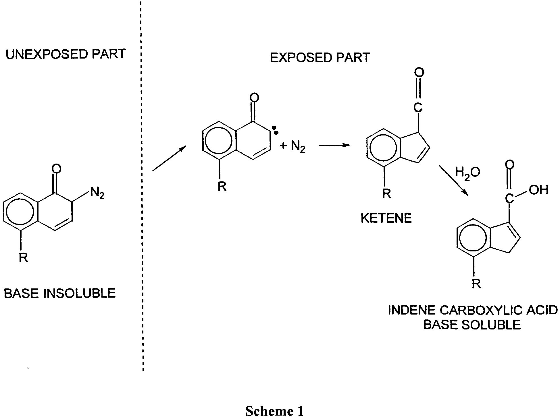
- As can be seen the base insoluble resin is transformed into a base soluble entity following exposure to light.
- The substrate to which the photoresist layer is applied can be any substrate which is capable of withstanding the pyrolysis or CVD (chemical vapour deposition) conditions employed, for nanotube growth and which is capable of supporting aligned carbon nanotube growth. Examples of suitable substrates include all types of glass that provide sufficient thermal stability according to the synthesis temperature applied, such as quartz glass, as well as alumina, graphite, mica, mesaporous silica, silicon water, nanoporous alumina or ceramic plates. Preferably the substrate is glass, in particular, quartz glass or silicon water. The substrate may also include a coating of a material which is capable of supporting carbon nanotube growth under the conditions employed. The coating may be of any metal, metaloxide, metal alloy or compound thereof, which may have conducting or semiconducting properties. Examples of suitable metals include Au, Pt, Cu, Cr, Ni, Fe, Co and Pd. Examples of suitable compounds are metal oxides, metal carbides, metal nitrides, metal sulfides and metal borides. Examples of suitable metal oxides include indium tin oxide (ITO), Al2O3, TiO2 and MgO. Examples of semiconducting materials include gallium arsenide, aluminium arsenide, aluminium sulphide and gallium sulphide.
- The patterning of the aligned carbon nanotubes is achieved by creating a region on the substrate which is incapable of supporting nanotube growth. The pattern is created on the substrate by applying an appropriate mask to the photoresist layer such that part of the photoresist layer is capable of being exposed to electromagnetic radiation, while the remaining photoresist layer is substantially shielded from such electromagnetic radiation. Depending on the solubility properties of the exposed and unexposed photoresist, the patterning of the subsequently synthesised aligned carbon nanotube layer will be defined by the positive or negative of the mask.
- One suitable mask is a quartz plate coated with a thin layer of metal micropatterns, where the regions covered by the thin metal layer are opaque while the uncovered areas are transparent to a photo-irradiation beam. The photomask may be applied to the photoresist layer by physical pressing.
- When the mask is applied to the photoresist layer the photoresist coated substrate is subjected to electromagnetic radiation to transform the exposed region of the photoresist. The transformation which is undergone by the photoresist will depend on the nature and properties of the photoresist. Accordingly the transformation may represent a polymerisation, an oxidation, or other chemical transformation of the photoresist material. The transformation should be specific to the exposed region, should result in a change in solubility characteristics relative to the unexposed photoresist, and should be sufficiently permanent to enable selective solubilisation of the exposed or the unexposed photoresist.
- The electromagnetic radiation used to irradiate the exposed photoresist will depend on the nature of the photoresist material used, however for most applications the electromagnetic radiation will be UV radiation.
- The photoresist layer is then developed by contact with a solvent which is capable of dissolving the portion of the photoresist layer which is to later support growth of aligned carbon nanotubes into the desired pattern. This will be either the exposed (transformed) region or the unexposed (untransformed) region. The contact with the solvent should be such that the non-dissolved region of the photoresist remains attached to the substrate.
- The nature of the solvent used will depend on the type of photoresist utilised and the nature of the transformation which it undergoes on exposure to electromagnetic radiation. In the case of cresol novolac resin (which is base insoluble) exposure to UV radiation produces a carboxylic acid moiety which is soluble in base. Accordingly the exposed region of the photoresist can be dissolved using aqueous solution of a suitable base, such as an alkali metal hydroxide, ammonium hydroxide, tetramethylammonium hydroxide. Alternatively a solvent can be selected which dissolves the unexposed region of the photoresist, such as ethylene glycol, butanediol, dimethyl ether, diethyl ether, methyl ethyl ether, acetone, methyl ethyl ketone. With other photoresists the selection of a suitable solvent may be made between polar solvents, such as water, ethanol, methanol, acetone and the like on the one hand and non-polar solvents, such as benzene, toluene and the like on the other hand. A person skilled in the art would be readily able to select a suitable solvent to dissolve the desired region of the photoresist.
- The next step in the process involves the synthesis of a layer of aligned carbon nanotubes on the region of the substrate from which the photoresist has been dissolved. This may be achieved using a suitable technique for the synthesis of perpendicularly aligned carbon nanotubes. Preferably the aligned carbon nanotubes are prepared by pyrolysis of a carbon-containing material in the presence of a suitable catalyst for nanotube formation.
- The carbon-containing material may be any compound or substance which includes carbon and which is capable for forming carbon nanotubes when subjected to pyrolysis in the presence of a suitable catalyst. Examples of suitable carbon-containing materials include alkanes, alkenes, alkynes or aromatic hydrocarbons and their derivatives, for example methane, acetylene, benzene, organometallic compounds of transition metals, for example transition metal phthalocyanines, such as Fe(II) phthalocyanine, and metallocenes such as ferrocene and nickel dicyclopentadiene and evaporable metal complex.
- The catalyst may be any compound, element or substance suitable for catalysing the conversion of a carbon-containing material to aligned carbon nanotubes under pyrolytic conditions. The catalyst may be a transition metal, such as Fe, Co, Al, Ni, Mn, Pd, Cr or alloys thereof in any suitable oxidation state.
- The catalyst may be incorporated into the substrate or may be included in the carbon-containing material. Examples of carbon-containing materials which include a transition metal catalyst are Fe(II) phthalocyanine, Ni(II) phthalocyanine and ferrocene. When the catalyst and carbon-containing material are included in the same material it may be necessary to provide sources of additional catalyst or additional carbon-containing material. For example, when ferrocene is used as the catalyst and a source of carbon, it is necessary to provide an additional carbon source, such as ethylene, to obtain the required nanotube growth.
- The pyrolysis condition employed will depend on the type of carbon-containing material employed and the type of catalyst, as well as the length and density of the nanotubes required. In this regard it is possible to vary the pyrolysis conditions, such as the temperature, time, pressure or flow rate through the pyrolysis reactor, to obtain nanotubes having different characteristics.
- For example, performing the pyrolysis at a higher temperature may produce nanotubes having different base-end structures relative to those prepared at a lower temperature. The pyrolysis will generally be performed with a temperature range of 500°C to 1100°C. Similarly lowering the flow rate through a flow-type pyrolysis reactor may result in a smaller packing density of the nanotubes and vice versa. A person skilled in the art would be able to select and control the conditions of pyrolysis to obtain nanotubes having the desired characteristics.
- After synthesis of the layer of aligned carbon nanotubes in the pattern array on the substrate, the photoresist material remaining on the substrate may be dissociated from the carbon nanotubes. This may be achieved using a solvent capable of dissolving the remaining photoresist layer. Alternatively it is possible to disassociate the carbon nanotubes from the substrate by transferring the patterned carbon nanotube layer to another substrate. This other substrate may be another substrate capable of supporting carbon nanotube growth, or may be a metal, metal oxide, semi-conductor material or a polymer. Examples of suitable polymers include adhesive coated polymers such as cellulose tape, conjugated (conducting) polymers, temperature/pressure responsive polymers, bioactive polymers and engineering resins.
- Where the patterned layer of aligned carbon nanotubes is transferred to another substrate which is capable of supporting carbon nanotube growth, it is possible to form a hetero-structured nanotube film by subjecting the nanotube coated substrate to conditions for promoting aligned carbon nanotube growth. The conditions of nanotube formation may be controlled or adjusted such that the length of the further nanotubes is different to the length of the nanotubes making up the original patterned layer. This second layer of nanotubes will tend to grow in the spaces defined by the original patterned layer. It may also be possible to adjust conditions such that there is some further nanotube growth on top of the original patterned layer.
- The nanotube patterns on quartz plates may also be separated from the substrate, while retaining the integrity of the pattern by immersing the sample in an aqueous hydrofluoric acid solution (10-40% w/w) for an appropriate period.
- For some applications, the patterned carbon nanotube film may be incorporated into a multilayer structure including layers of other materials, such as metals, metal oxides, semiconductor materials or polymers.
- The patterned carbon nanotube film prepared in accordance with the present invention and the devices including these patterned films represent further aspects of the present invention.
- The patterned film prepared in accordance with any one of the processes of the present invention and devices, materials coated with or including these multilayer films represent further aspects of the present invention.
- As is evident from the above description the invention allows the preparation of a large variety of patterned films and structures. The processes of the present invention and the patterned structures formed may have use in the following applications:
- 1) electron emitters
- 2) field-emission transistors
- 3) electrodes for photovoltaic cells and light emitting diodes with region-specific characteristics
- 4) optoelectronic elements
- 5) bismuth actuators
- 7) chemical and biological sensors with region-specific characteristics
- 8) gas storages
- 9) molecular-filtration membranes
- 10) region-specific energy absorbing materials.
- The invention will now be described with reference to the following examples and drawings which illustrate some preferred embodiments of the invention. However it should be understood that the particularity of the following description is not to supersede the generality of the invention previously described.
- Referring to the drawings:
-
Figure 1 is a diagrammatic representation of a pyrolysis flow reactor suitable for preparing aligned carbon nanotubes. -
Figure 2a is a scanning electron microscopic image of aligned carbon nanotubes on a quartz glass substrate. -
Figure 2b is a high resolution transmission electron microscopic image of an individual carbon nanotube. -
Figure 3 is a schematic diagram showing the stages involved in the preparation of a patterned layer of aligned carbon nanotubes according to the embodiment of the invention. -
Figure 4 is a scanning electron microscopic image of a patterned layer of aligned carbon nanotubes. - Aligned carbon nanotubes were prepared by pyrolysis of iron (II) phthalocyanine under Ar/H2 at 800-1100°C using a quartz plate in a flow reactor consisting of a quartz glass tube and a dual furnace fitted with independent temperature controllers (
Figure 1 ).Figure 2a represents a typical scanning electron microscopic (SEM, XL-30 FEG SEM, Philips, at 5 KV) image of the carbon nanotubes, showing that the as-synthesised nanotubes align almost normal to the substrate surface. The aligned nanotubes are densely packed with a fairly uniform tubular length of ca. 25 µm. However, the length of the aligned nanotubes can be varied over a wide range (from a few to several tens of micrometers) in a controllable fashion by changing the experimental conditions (e.g. the pyrolysis time, flow rate). A well-graphitised structure with ca. 40 concentric carbon shells and an outer diameter of ca. 40 nm is illustrated in the high resolution transmission electron microscopic HR-TEM, CM30, Philips, at 300 KV) image of an individual nanotube (Figure 2b ). - In this example cresol novolac resin was used as a positive photoresist. The indene carboxylic acid derivative of the photoresist formed in regions exposed to UV is base soluble while the unexposed photoresist remains to be insoluble under the same conditions. The steps involved in forming the pattern are shown schematically in
Figure 3 . A photoresist solution was prepared by dissolving 30g of naphthoquinone diazid-cresol novolac resin in 100 mL ethoxy ethyl acetate. Spin-casting of the photoresist solution onto a quartz glass plate resulted in the formation of a photoresist coating, which was baked in an oven at 80°C for 10 min. The resultant dry photoresist layer (0.2 µm thick) was then exposed through a photomask to EIMAC, VARIAN R150-8 at a lamp-sample distance of 111cm for 30 sec. The photoresist was then developed in a 1% sodium hydroxide solution for 8 sec. After rinsing with distilled water, the photoresist patterned quartz plate was further baked at 80°C for 10 min. - The photoresist prepatterned quartz plate prepared in Example 2 was used for growing the aligned nanotubes in accordance with the process described in Example 1. The aligned nanotube pattern thus prepared is shown in
Figure 4 , the nanotube pattern showing a close replication of the photomask structure. As seen inFigure 4 , aligned nanotube bundles at a submicrometer scale are clearly evident. - Throughout this specification and the claims which follow, unless the context requires otherwise, the word "comprise", and variations such as "comprises" and "comprising", will be understood to imply the inclusion of a stated integer or step or group of integers or steps but not the exclusion of any other integer or step or group of integers or steps.
Claims (35)
- A process for preparing a patterned layer of aligned carbon nanotubes on a substrate including:applying a photoresist layer to at least a portion of a surface of a substrate capable of supporting nanotube growth,masking a region of said photoresist layer to provide a masked portion and an unmasked portion,subjecting said unmasked portion to electromagnetic radiation of a wavelength and intensity sufficient to transform the unmasked portion while leaving the masked portion substantially untransformed, said transformed portion exhibiting solubility characteristics different to said untransformed portion,developing said photoresist layer by contacting with a solvent for a time and under conditions sufficient to dissolve one of said transformed and untransformed portions of the photoresist, leaving the other portion attached to said substrate,synthesising a layer of aligned carbon nanotubes on regions of said substrate to which said remaining photoresist portion is not attached to provide a patterned layer of aligned carbon nanotubes on said substrate.
- The process according to claim 1 wherein the photoresist layer is selected from the group consisting of diazonaphthoquinone (DNQ)-based photoresists, epoxy resins, polyanilines, polymethyl methacrylate, polystyrenes, and polydienes.
- The process according to claim 2 wherein the photoresist layer is cresol novolac resin.
- The process according to claim 1 wherein the substrate is selected from the group consisting of quartz glass, mesoporous silica, silicon water, nanoporous alumina, ceramic plates, graphite and mica.
- The process according to claim 4 wherein the substrate is quartz glass or silicon water.
- The process according to claim 1 wherein the substrate comprises a coating of a material which is capable of supporting carbon nanotube growth under the conditions employed.
- The process according to claim 6 wherein the coating is selected from the group consisting of a metal, metal alloy or compound thereof having conducting or semiconducting properties.
- The process according to claim 7 wherein the coating is a metal selected from the group consisting of Au, Pt, Cu, Cr, Ni, Fe, Co and Pd.
- The process according to claim 7 wherein the coating is a metal compound or metal alloy compound selected from an oxide, a carbide, a nitride, a sulfide or a boride.
- The process according to claim 9 wherein the coating is a metal oxide selected from the group consisting of indium tin oxide (ITO), Al2O3, TiO2 and MgO.
- The process according to claim 7 wherein the coating is a semiconducting material selected from the group consisting of gallium arsenide, aluminium arsenide, aluminium sulphide and gallium sulphide.
- The process of claim 1 wherein the electromagnetic radiation is UV radiation.
- The process according to claim 3 wherein the solvent is a base and the transformed portion of the photoresist layer is dissolved.
- The process according to claim 13 wherein the base is selected from the group consisting of alkali metal hydroxide, ammonium hydroxide and tetramethylammonium hydroxide.
- The process according to claim 3 wherein the solvent dissolves the untransformed portion of the photoresist layer.
- The process according to claim 15 wherein the solvent is selected from the group consisting of ethylene glycol, butanediol, dimethyl ether, diethyl ether, methyl ethyl ether, acetone and methyl ethyl ketone.
- The process according to claim 1 wherein the aligned carbon nanotubes are synthesised by pyrolysis of a carbon-containing material in the presence of a suitable catalyst for nanotube formation.
- The process according to claim 17 wherein the carbon-containing material is selected from alkanes, alkenes, alkynes or aromatic hydrocarbons and their derivatives, organometallic compounds of transition metals and evaporable metal complexes.
- The process according to claim 18 wherein the carbon-containing material is selected from methane, acetylene and benzene.
- The process according to claim 18 wherein the organometallic compound is a transition metal phthalocyanine.
- The process according to claim 18 wherein the organometallic compound is a metallocene.
- The process according to claim 17 wherein the catalyst is a transition metal.
- The process according to claim 22 wherein the transition metal is selected from the group consisting of Fe, Co, Al, Ni, Mn, Pd, Cr or alloys thereof in any suitable oxidation state.
- The process according to claim 17 wherein the catalyst is incorporated in the carbon-containing material.
- The process according to claim 24 wherein the catalyst is selected from the group consisting of Fe(II) phthalocyanine, Ni(II) phthalocyanine and ferrocene.
- The process according to claim 24 further comprising an additional source of catalyst.
- The process according to claim 24 further comprising an additional source of carbon-containing material.
- The process according to claim 17 wherein the pyrolysis is carried out at 500°C to 1100°C.
- The process according to claim 1 wherein the process comprises the further step of dissociating the aligned carbon nanotubes from the substrate.
- The process according to claim 29 wherein dissociation occurs by dissolving the remaining photoresist layer.
- The process according to claim 29 wherein the substrate is quartz glass and dissociation is effected by immersing the sample in an aqueous hydrofluoric acid solution (10-40% w/w).
- The process according to claim 29 wherein dissociation comprises transferring the patterned carbon nanotube layer to another substrate.
- The process according to claim 32 wherein the other substrate is selected from the group consisting of another substrate capable of supporting carbon nanotube growth, a metal, metal oxide, semi-conductor material or a polymer.
- The process according to claim 33 wherein the polymer is selected from the group consisting of adhesive coated polymers, conjugated (conducting) polymers, temperature/pressure responsive polymers, bioactive polymers and engineering resins.
- The process according to claim 34 wherein the adhesive coated polymer is cellulose tape.
Applications Claiming Priority (3)
| Application Number | Priority Date | Filing Date | Title |
|---|---|---|---|
| AUPQ0649A AUPQ064999A0 (en) | 1999-05-28 | 1999-05-28 | Patterned carbon nanotube films |
| AUPQ064999 | 1999-05-28 | ||
| PCT/AU2000/000549 WO2000073203A1 (en) | 1999-05-28 | 2000-05-25 | Patterned carbon nanotube films |
Publications (3)
| Publication Number | Publication Date |
|---|---|
| EP1200341A1 EP1200341A1 (en) | 2002-05-02 |
| EP1200341A4 EP1200341A4 (en) | 2007-08-08 |
| EP1200341B1 true EP1200341B1 (en) | 2012-07-11 |
Family
ID=3814849
Family Applications (1)
| Application Number | Title | Priority Date | Filing Date |
|---|---|---|---|
| EP00926580A Expired - Lifetime EP1200341B1 (en) | 1999-05-28 | 2000-05-25 | Patterned carbon nanotube films |
Country Status (5)
| Country | Link |
|---|---|
| US (1) | US6811957B1 (en) |
| EP (1) | EP1200341B1 (en) |
| JP (1) | JP2003500324A (en) |
| AU (1) | AUPQ064999A0 (en) |
| WO (1) | WO2000073203A1 (en) |
Cited By (1)
| Publication number | Priority date | Publication date | Assignee | Title |
|---|---|---|---|---|
| CN103951940A (en) * | 2014-04-10 | 2014-07-30 | 惠州学院 | Antistatic epoxy resin composite material and preparation method thereof |
Families Citing this family (51)
| Publication number | Priority date | Publication date | Assignee | Title |
|---|---|---|---|---|
| AUPQ304199A0 (en) * | 1999-09-23 | 1999-10-21 | Commonwealth Scientific And Industrial Research Organisation | Patterned carbon nanotubes |
| WO2002080195A1 (en) * | 2001-02-16 | 2002-10-10 | E.I. Dupont De Nemours And Company | High conductivity polyaniline compositions and uses therefor |
| DE10113549C2 (en) * | 2001-03-20 | 2003-02-06 | Infineon Technologies Ag | Process for growing nanotubes |
| AUPR421701A0 (en) | 2001-04-04 | 2001-05-17 | Commonwealth Scientific And Industrial Research Organisation | Process and apparatus for the production of carbon nanotubes |
| AU2002245939B2 (en) * | 2001-04-04 | 2006-05-11 | Commonwealth Scientific And Industrial Research Organisation | Process and apparatus for the production of carbon nanotubes |
| CA2450778A1 (en) | 2001-06-14 | 2003-10-16 | Hyperion Catalysis International, Inc. | Field emission devices using modified carbon nanotubes |
| WO2002103737A2 (en) | 2001-06-14 | 2002-12-27 | Hyperion Catalysis International, Inc. | Field emission devices using ion bombarded carbon nanotubes |
| US7341498B2 (en) | 2001-06-14 | 2008-03-11 | Hyperion Catalysis International, Inc. | Method of irradiating field emission cathode having nanotubes |
| RU2225835C2 (en) * | 2001-08-10 | 2004-03-20 | Институт прикладной механики УрО РАН | Method of preparing carbon and metal-containing nanostructures |
| US6891319B2 (en) | 2001-08-29 | 2005-05-10 | Motorola, Inc. | Field emission display and methods of forming a field emission display |
| US7070472B2 (en) | 2001-08-29 | 2006-07-04 | Motorola, Inc. | Field emission display and methods of forming a field emission display |
| US7318908B1 (en) * | 2001-11-01 | 2008-01-15 | The Board Of Trustees Of The Leland Stanford Junior University | Integrated nanotube sensor |
| GB0226590D0 (en) * | 2002-11-14 | 2002-12-24 | Univ Cambridge Tech | Method for producing carbon nanotubes and/or nanofibres |
| KR100801820B1 (en) * | 2002-11-19 | 2008-02-11 | 삼성전자주식회사 | Pattern Forming Method Using Surface-Modified Carbon Nanotubes |
| US7579077B2 (en) * | 2003-05-05 | 2009-08-25 | Nanosys, Inc. | Nanofiber surfaces for use in enhanced surface area applications |
| US7972616B2 (en) * | 2003-04-17 | 2011-07-05 | Nanosys, Inc. | Medical device applications of nanostructured surfaces |
| TWI427709B (en) * | 2003-05-05 | 2014-02-21 | Nanosys Inc | Nanofiber surfaces for use in enhanced surface area applications |
| US7803574B2 (en) | 2003-05-05 | 2010-09-28 | Nanosys, Inc. | Medical device applications of nanostructured surfaces |
| US7067237B2 (en) * | 2003-06-28 | 2006-06-27 | Samsung Electronics Co., Ltd. | Method for forming pattern of one-dimensional nanostructure |
| US8541054B2 (en) | 2003-09-08 | 2013-09-24 | Honda Motor Co., Ltd | Methods for preparation of one-dimensional carbon nanostructures |
| JP2007504086A (en) * | 2003-09-03 | 2007-03-01 | 本田技研工業株式会社 | Method for producing one-dimensional carbon nanostructure |
| DE10345755B4 (en) * | 2003-09-25 | 2006-08-31 | Leibniz-Institut Für Festkörper- Und Werkstoffforschung Dresden E.V. | Process for the preparation of structured magnetic functional elements |
| US7067328B2 (en) | 2003-09-25 | 2006-06-27 | Nanosys, Inc. | Methods, devices and compositions for depositing and orienting nanostructures |
| CN1307092C (en) * | 2004-02-12 | 2007-03-28 | 鸿富锦精密工业(深圳)有限公司 | Manufacturing method of nanometer carbon tube |
| JP2008511985A (en) * | 2004-08-31 | 2008-04-17 | エージェンシー フォー サイエンス,テクノロジー アンド リサーチ | Nanostructure and method for producing the same |
| JP2006181699A (en) * | 2004-12-28 | 2006-07-13 | Kumamoto Technology & Industry Foundation | Carbon molecular structure manufacturing method, carbon molecular structure, diode, active device, and integrated circuit |
| US20080199389A1 (en) * | 2005-05-23 | 2008-08-21 | Chiu Wilson K S | Method and device for producing carbon nanotubes |
| KR20070046611A (en) * | 2005-10-31 | 2007-05-03 | 삼성에스디아이 주식회사 | Electron emission source with a protective film and an electron emission device including the same |
| US20070298168A1 (en) * | 2006-06-09 | 2007-12-27 | Rensselaer Polytechnic Institute | Multifunctional carbon nanotube based brushes |
| US20080136861A1 (en) * | 2006-12-11 | 2008-06-12 | 3M Innovative Properties Company | Method and apparatus for printing conductive inks |
| US8319002B2 (en) * | 2007-12-06 | 2012-11-27 | Nanosys, Inc. | Nanostructure-enhanced platelet binding and hemostatic structures |
| US8304595B2 (en) | 2007-12-06 | 2012-11-06 | Nanosys, Inc. | Resorbable nanoenhanced hemostatic structures and bandage materials |
| KR101410929B1 (en) * | 2008-01-17 | 2014-06-23 | 삼성전자주식회사 | Method of transferring carbon nanotubes |
| US9318295B2 (en) * | 2008-01-18 | 2016-04-19 | The United States Of America As Represented By The Administrator Of The Nasa | Carbon nanotube patterning on a metal substrate |
| CN101671442A (en) * | 2008-09-12 | 2010-03-17 | 清华大学 | Preparation method of carbon nano tube array composite material |
| KR101049798B1 (en) | 2009-09-14 | 2011-07-19 | 한국화학연구원 | Mass production method of single layer carbon nanotube transistor |
| WO2011109473A1 (en) * | 2010-03-02 | 2011-09-09 | The Ohio State University Research Foundation | Molecularly imprinted carbon |
| US8491970B2 (en) * | 2010-09-29 | 2013-07-23 | Teledyne Scientific & Imaging, Llc | Vertically aligned carbon nanotube arrays from liquid dispersions |
| EA201100820A1 (en) * | 2011-06-01 | 2012-05-30 | Федеральное Государственное Учреждение "Научно-Производственный Комплекс "Технологический Центр" Московского Государственного Института Электронной Техники" | METHOD OF FORMING MASSIVES OF CARBON NANOTUBES |
| US9336919B2 (en) | 2012-08-17 | 2016-05-10 | The Trustees Of The University Of Pennsylvania | Methods for preparing colloidal nanocrystal-based thin films |
| WO2014113655A2 (en) * | 2013-01-18 | 2014-07-24 | The Trustees Of The University Of Pennsylvania | Nanocrystal thin film device fabrication methods and apparatus |
| WO2015128804A1 (en) * | 2014-02-27 | 2015-09-03 | Indian Institute Of Technology Kanpur | Nanobrushes and methods of manufacture and use |
| US20210122627A1 (en) * | 2014-09-16 | 2021-04-29 | San Diego State University Research Foundation | Hybrid Metal and Carbon or Glassy Carbon MEMS u-ECOG Electrode and Microelectrode Structures |
| US9520258B2 (en) * | 2015-01-28 | 2016-12-13 | Eloret Corporation | Selective synthesis of nanotubes without inhibitor |
| CN105510400B (en) * | 2015-11-30 | 2018-09-07 | 电子科技大学 | A kind of hydrogen gas sensor based on carbon nanotube and palladium laminated film |
| US10343920B2 (en) * | 2016-03-18 | 2019-07-09 | Asm Ip Holding B.V. | Aligned carbon nanotubes |
| CN108132582B (en) | 2016-12-01 | 2020-06-09 | 清华大学 | Photolithography Mask |
| CN108132579B (en) | 2016-12-01 | 2020-09-25 | 清华大学 | Photolithography Mask |
| CN108132585B (en) | 2016-12-01 | 2020-02-07 | 清华大学 | Preparation method of micro-nano structure |
| CN108132581B (en) | 2016-12-01 | 2020-07-10 | 清华大学 | Photolithography Mask |
| CN110668426A (en) * | 2019-11-20 | 2020-01-10 | 国网重庆市电力公司电力科学研究院 | A method for preparing aluminum-doped carbon nanotubes |
Family Cites Families (10)
| Publication number | Priority date | Publication date | Assignee | Title |
|---|---|---|---|---|
| JP3365874B2 (en) * | 1994-10-05 | 2003-01-14 | 富士写真フイルム株式会社 | Synthetic method of quinonediazide and positive resist containing the same |
| JP2969503B2 (en) * | 1996-02-15 | 1999-11-02 | 科学技術振興事業団 | How to make carbonaceous fiber |
| US5872422A (en) | 1995-12-20 | 1999-02-16 | Advanced Technology Materials, Inc. | Carbon fiber-based field emission devices |
| AU3367697A (en) * | 1996-05-06 | 1997-11-26 | University Of Washington | Virtual motion controller |
| US5726524A (en) * | 1996-05-31 | 1998-03-10 | Minnesota Mining And Manufacturing Company | Field emission device having nanostructured emitters |
| JP3421549B2 (en) * | 1996-09-18 | 2003-06-30 | 株式会社東芝 | Vacuum micro device |
| JP3183845B2 (en) * | 1997-03-21 | 2001-07-09 | 財団法人ファインセラミックスセンター | Method for producing carbon nanotube and carbon nanotube film |
| JP3441923B2 (en) * | 1997-06-18 | 2003-09-02 | キヤノン株式会社 | Manufacturing method of carbon nanotube |
| KR20010074667A (en) | 1998-06-19 | 2001-08-08 | 추후보정 | Free-standing and aligned carbon nanotubes and synthesis thereof |
| US6062931A (en) * | 1999-09-01 | 2000-05-16 | Industrial Technology Research Institute | Carbon nanotube emitter with triode structure |
-
1999
- 1999-05-28 AU AUPQ0649A patent/AUPQ064999A0/en not_active Abandoned
-
2000
- 2000-05-25 JP JP2000621279A patent/JP2003500324A/en active Pending
- 2000-05-25 US US09/979,793 patent/US6811957B1/en not_active Expired - Lifetime
- 2000-05-25 WO PCT/AU2000/000549 patent/WO2000073203A1/en not_active Ceased
- 2000-05-25 EP EP00926580A patent/EP1200341B1/en not_active Expired - Lifetime
Cited By (1)
| Publication number | Priority date | Publication date | Assignee | Title |
|---|---|---|---|---|
| CN103951940A (en) * | 2014-04-10 | 2014-07-30 | 惠州学院 | Antistatic epoxy resin composite material and preparation method thereof |
Also Published As
| Publication number | Publication date |
|---|---|
| JP2003500324A (en) | 2003-01-07 |
| WO2000073203A1 (en) | 2000-12-07 |
| US6811957B1 (en) | 2004-11-02 |
| EP1200341A4 (en) | 2007-08-08 |
| AUPQ064999A0 (en) | 1999-06-24 |
| EP1200341A1 (en) | 2002-05-02 |
Similar Documents
| Publication | Publication Date | Title |
|---|---|---|
| US6811957B1 (en) | Patterned carbon nanotube films | |
| US6866801B1 (en) | Process for making aligned carbon nanotubes | |
| US7799163B1 (en) | Substrate-supported aligned carbon nanotube films | |
| EP1506938B1 (en) | Method for manufacturing a carbon nanotube structure and carbon nanotube transfer body | |
| US6998358B2 (en) | Method for providing nano-structures of uniform length | |
| CN1898804B (en) | Rectification element, electronic circuit using same, and method of manufacturing rectification element | |
| KR20020024580A (en) | Multilayer carbon nanotube films | |
| CN100543895C (en) | Electronic component and electronic device and manufacturing method thereof | |
| US8541054B2 (en) | Methods for preparation of one-dimensional carbon nanostructures | |
| JP5437305B2 (en) | Method for producing one-dimensional carbon nanostructure | |
| CN1721323A (en) | Method for preparing basal catalyst and method for preparing carbon nanometer tube using the catalyst | |
| AU753177B2 (en) | Patterned carbon nanotube films | |
| AU776402C (en) | Patterned carbon nanotubes | |
| Huang et al. | Aligned carbon nanotubes patterned photolithographically by silver | |
| US20060216636A1 (en) | Catalytic resist including metal precursor compound and method of patterning catalyst particles using the same | |
| US7718224B2 (en) | Synthesis of single-walled carbon nanotubes | |
| AU3649600A (en) | Multilayer carbon nanotube films | |
| AU759314B2 (en) | Substrate-supported aligned carbon nanotube films |
Legal Events
| Date | Code | Title | Description |
|---|---|---|---|
| PUAI | Public reference made under article 153(3) epc to a published international application that has entered the european phase |
Free format text: ORIGINAL CODE: 0009012 |
|
| 17P | Request for examination filed |
Effective date: 20011127 |
|
| AK | Designated contracting states |
Kind code of ref document: A1 Designated state(s): AT BE CH CY DE DK ES FI FR GB GR IE IT LI LU MC NL PT SE |
|
| AX | Request for extension of the european patent |
Free format text: AL;LT;LV;MK;RO;SI |
|
| RAP1 | Party data changed (applicant data changed or rights of an application transferred) |
Owner name: UNIVERSITY OF DAYTON |
|
| A4 | Supplementary search report drawn up and despatched |
Effective date: 20070705 |
|
| RIC1 | Information provided on ipc code assigned before grant |
Ipc: C01B 31/02 20060101AFI20001213BHEP Ipc: G03F 7/00 20060101ALI20070629BHEP |
|
| 17Q | First examination report despatched |
Effective date: 20071121 |
|
| RIC1 | Information provided on ipc code assigned before grant |
Ipc: G03F 7/40 20060101ALI20110921BHEP Ipc: C01B 31/02 20060101AFI20110921BHEP |
|
| GRAP | Despatch of communication of intention to grant a patent |
Free format text: ORIGINAL CODE: EPIDOSNIGR1 |
|
| GRAS | Grant fee paid |
Free format text: ORIGINAL CODE: EPIDOSNIGR3 |
|
| GRAA | (expected) grant |
Free format text: ORIGINAL CODE: 0009210 |
|
| AK | Designated contracting states |
Kind code of ref document: B1 Designated state(s): AT BE CH CY DE DK ES FI FR GB GR IE IT LI LU MC NL PT SE |
|
| REG | Reference to a national code |
Ref country code: GB Ref legal event code: FG4D |
|
| REG | Reference to a national code |
Ref country code: CH Ref legal event code: EP |
|
| REG | Reference to a national code |
Ref country code: AT Ref legal event code: REF Ref document number: 566039 Country of ref document: AT Kind code of ref document: T Effective date: 20120715 |
|
| REG | Reference to a national code |
Ref country code: IE Ref legal event code: FG4D |
|
| REG | Reference to a national code |
Ref country code: DE Ref legal event code: R096 Ref document number: 60047339 Country of ref document: DE Effective date: 20120906 |
|
| REG | Reference to a national code |
Ref country code: NL Ref legal event code: VDEP Effective date: 20120711 |
|
| REG | Reference to a national code |
Ref country code: AT Ref legal event code: MK05 Ref document number: 566039 Country of ref document: AT Kind code of ref document: T Effective date: 20120711 |
|
| PG25 | Lapsed in a contracting state [announced via postgrant information from national office to epo] |
Ref country code: BE Free format text: LAPSE BECAUSE OF FAILURE TO SUBMIT A TRANSLATION OF THE DESCRIPTION OR TO PAY THE FEE WITHIN THE PRESCRIBED TIME-LIMIT Effective date: 20120711 Ref country code: FI Free format text: LAPSE BECAUSE OF FAILURE TO SUBMIT A TRANSLATION OF THE DESCRIPTION OR TO PAY THE FEE WITHIN THE PRESCRIBED TIME-LIMIT Effective date: 20120711 Ref country code: AT Free format text: LAPSE BECAUSE OF FAILURE TO SUBMIT A TRANSLATION OF THE DESCRIPTION OR TO PAY THE FEE WITHIN THE PRESCRIBED TIME-LIMIT Effective date: 20120711 Ref country code: CY Free format text: LAPSE BECAUSE OF FAILURE TO SUBMIT A TRANSLATION OF THE DESCRIPTION OR TO PAY THE FEE WITHIN THE PRESCRIBED TIME-LIMIT Effective date: 20120711 |
|
| PG25 | Lapsed in a contracting state [announced via postgrant information from national office to epo] |
Ref country code: PT Free format text: LAPSE BECAUSE OF FAILURE TO SUBMIT A TRANSLATION OF THE DESCRIPTION OR TO PAY THE FEE WITHIN THE PRESCRIBED TIME-LIMIT Effective date: 20121112 Ref country code: SE Free format text: LAPSE BECAUSE OF FAILURE TO SUBMIT A TRANSLATION OF THE DESCRIPTION OR TO PAY THE FEE WITHIN THE PRESCRIBED TIME-LIMIT Effective date: 20120711 Ref country code: GR Free format text: LAPSE BECAUSE OF FAILURE TO SUBMIT A TRANSLATION OF THE DESCRIPTION OR TO PAY THE FEE WITHIN THE PRESCRIBED TIME-LIMIT Effective date: 20121012 |
|
| PG25 | Lapsed in a contracting state [announced via postgrant information from national office to epo] |
Ref country code: NL Free format text: LAPSE BECAUSE OF FAILURE TO SUBMIT A TRANSLATION OF THE DESCRIPTION OR TO PAY THE FEE WITHIN THE PRESCRIBED TIME-LIMIT Effective date: 20120711 |
|
| PG25 | Lapsed in a contracting state [announced via postgrant information from national office to epo] |
Ref country code: ES Free format text: LAPSE BECAUSE OF FAILURE TO SUBMIT A TRANSLATION OF THE DESCRIPTION OR TO PAY THE FEE WITHIN THE PRESCRIBED TIME-LIMIT Effective date: 20121022 Ref country code: DK Free format text: LAPSE BECAUSE OF FAILURE TO SUBMIT A TRANSLATION OF THE DESCRIPTION OR TO PAY THE FEE WITHIN THE PRESCRIBED TIME-LIMIT Effective date: 20120711 |
|
| PLBE | No opposition filed within time limit |
Free format text: ORIGINAL CODE: 0009261 |
|
| STAA | Information on the status of an ep patent application or granted ep patent |
Free format text: STATUS: NO OPPOSITION FILED WITHIN TIME LIMIT |
|
| PG25 | Lapsed in a contracting state [announced via postgrant information from national office to epo] |
Ref country code: IT Free format text: LAPSE BECAUSE OF FAILURE TO SUBMIT A TRANSLATION OF THE DESCRIPTION OR TO PAY THE FEE WITHIN THE PRESCRIBED TIME-LIMIT Effective date: 20120711 |
|
| 26N | No opposition filed |
Effective date: 20130412 |
|
| REG | Reference to a national code |
Ref country code: DE Ref legal event code: R097 Ref document number: 60047339 Country of ref document: DE Effective date: 20130412 |
|
| PG25 | Lapsed in a contracting state [announced via postgrant information from national office to epo] |
Ref country code: MC Free format text: LAPSE BECAUSE OF FAILURE TO SUBMIT A TRANSLATION OF THE DESCRIPTION OR TO PAY THE FEE WITHIN THE PRESCRIBED TIME-LIMIT Effective date: 20120711 |
|
| REG | Reference to a national code |
Ref country code: CH Ref legal event code: PL |
|
| GBPC | Gb: european patent ceased through non-payment of renewal fee |
Effective date: 20130525 |
|
| PG25 | Lapsed in a contracting state [announced via postgrant information from national office to epo] |
Ref country code: CH Free format text: LAPSE BECAUSE OF NON-PAYMENT OF DUE FEES Effective date: 20130531 Ref country code: LI Free format text: LAPSE BECAUSE OF NON-PAYMENT OF DUE FEES Effective date: 20130531 |
|
| REG | Reference to a national code |
Ref country code: IE Ref legal event code: MM4A |
|
| REG | Reference to a national code |
Ref country code: FR Ref legal event code: ST Effective date: 20140131 |
|
| PG25 | Lapsed in a contracting state [announced via postgrant information from national office to epo] |
Ref country code: GB Free format text: LAPSE BECAUSE OF NON-PAYMENT OF DUE FEES Effective date: 20130525 Ref country code: IE Free format text: LAPSE BECAUSE OF NON-PAYMENT OF DUE FEES Effective date: 20130525 |
|
| PG25 | Lapsed in a contracting state [announced via postgrant information from national office to epo] |
Ref country code: FR Free format text: LAPSE BECAUSE OF NON-PAYMENT OF DUE FEES Effective date: 20130531 |
|
| PGFP | Annual fee paid to national office [announced via postgrant information from national office to epo] |
Ref country code: DE Payment date: 20140529 Year of fee payment: 15 |
|
| PG25 | Lapsed in a contracting state [announced via postgrant information from national office to epo] |
Ref country code: LU Free format text: LAPSE BECAUSE OF NON-PAYMENT OF DUE FEES Effective date: 20130525 |
|
| REG | Reference to a national code |
Ref country code: DE Ref legal event code: R119 Ref document number: 60047339 Country of ref document: DE |
|
| PG25 | Lapsed in a contracting state [announced via postgrant information from national office to epo] |
Ref country code: DE Free format text: LAPSE BECAUSE OF NON-PAYMENT OF DUE FEES Effective date: 20151201 |