EP1199859A2 - Apparatus and method for generating transmission and reception local oscillation signals in a mobile terminal - Google Patents
Apparatus and method for generating transmission and reception local oscillation signals in a mobile terminal Download PDFInfo
- Publication number
- EP1199859A2 EP1199859A2 EP01124982A EP01124982A EP1199859A2 EP 1199859 A2 EP1199859 A2 EP 1199859A2 EP 01124982 A EP01124982 A EP 01124982A EP 01124982 A EP01124982 A EP 01124982A EP 1199859 A2 EP1199859 A2 EP 1199859A2
- Authority
- EP
- European Patent Office
- Prior art keywords
- pll
- local oscillation
- pll block
- block
- reception
- Prior art date
- Legal status (The legal status is an assumption and is not a legal conclusion. Google has not performed a legal analysis and makes no representation as to the accuracy of the status listed.)
- Ceased
Links
Images


Classifications
-
- H—ELECTRICITY
- H03—ELECTRONIC CIRCUITRY
- H03L—AUTOMATIC CONTROL, STARTING, SYNCHRONISATION OR STABILISATION OF GENERATORS OF ELECTRONIC OSCILLATIONS OR PULSES
- H03L7/00—Automatic control of frequency or phase; Synchronisation
- H03L7/06—Automatic control of frequency or phase; Synchronisation using a reference signal applied to a frequency- or phase-locked loop
- H03L7/08—Details of the phase-locked loop
- H03L7/099—Details of the phase-locked loop concerning mainly the controlled oscillator of the loop
-
- H—ELECTRICITY
- H04—ELECTRIC COMMUNICATION TECHNIQUE
- H04L—TRANSMISSION OF DIGITAL INFORMATION, e.g. TELEGRAPHIC COMMUNICATION
- H04L27/00—Modulated-carrier systems
- H04L27/0014—Carrier regulation
-
- H—ELECTRICITY
- H03—ELECTRONIC CIRCUITRY
- H03L—AUTOMATIC CONTROL, STARTING, SYNCHRONISATION OR STABILISATION OF GENERATORS OF ELECTRONIC OSCILLATIONS OR PULSES
- H03L7/00—Automatic control of frequency or phase; Synchronisation
- H03L7/06—Automatic control of frequency or phase; Synchronisation using a reference signal applied to a frequency- or phase-locked loop
- H03L7/16—Indirect frequency synthesis, i.e. generating a desired one of a number of predetermined frequencies using a frequency- or phase-locked loop
- H03L7/18—Indirect frequency synthesis, i.e. generating a desired one of a number of predetermined frequencies using a frequency- or phase-locked loop using a frequency divider or counter in the loop
- H03L7/197—Indirect frequency synthesis, i.e. generating a desired one of a number of predetermined frequencies using a frequency- or phase-locked loop using a frequency divider or counter in the loop a time difference being used for locking the loop, the counter counting between numbers which are variable in time or the frequency divider dividing by a factor variable in time, e.g. for obtaining fractional frequency division
- H03L7/1972—Indirect frequency synthesis, i.e. generating a desired one of a number of predetermined frequencies using a frequency- or phase-locked loop using a frequency divider or counter in the loop a time difference being used for locking the loop, the counter counting between numbers which are variable in time or the frequency divider dividing by a factor variable in time, e.g. for obtaining fractional frequency division for reducing the locking time interval
-
- H—ELECTRICITY
- H04—ELECTRIC COMMUNICATION TECHNIQUE
- H04B—TRANSMISSION
- H04B1/00—Details of transmission systems, not covered by a single one of groups H04B3/00 - H04B13/00; Details of transmission systems not characterised by the medium used for transmission
- H04B1/38—Transceivers, i.e. devices in which transmitter and receiver form a structural unit and in which at least one part is used for functions of transmitting and receiving
- H04B1/40—Circuits
- H04B1/403—Circuits using the same oscillator for generating both the transmitter frequency and the receiver local oscillator frequency
-
- H—ELECTRICITY
- H04—ELECTRIC COMMUNICATION TECHNIQUE
- H04L—TRANSMISSION OF DIGITAL INFORMATION, e.g. TELEGRAPHIC COMMUNICATION
- H04L27/00—Modulated-carrier systems
- H04L27/0014—Carrier regulation
- H04L2027/0016—Stabilisation of local oscillators
Definitions
- the present invention relates generally to a mobile terminal, and in particular, to an apparatus and method for generating transmission and reception local oscillation signals.
- a local oscillation signal for transmission (TX local oscillation signal) is used to upconvert the frequency of a transmission signal, whereas a local oscillation signal for reception (RX local oscillation signal) is used to downconvert the frequency of a received signal.
- the TX and RX local oscillation signals are generated by a PLL (Phase Locked Loop) block and provided to a radio transmitter and a radio receiver, respectively.
- PLL Phase Locked Loop
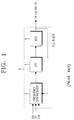
- a TX local oscillation signal and an RX local oscillation signal are selectively provided by a PLL block 8 as shown in FIG. 1.
- the PLL block 8 synchronizes the frequency and phase of its output signal to those of a reference signal or an input signal.
- the PLL block 8 is comprised of a frequency synthesizer 2, a low pass filter (LPF) 4, and a voltage controlled oscillator (VCO) 6.
- a controller (not shown) feeds an enable signal EN, data DT, a clock signal CLK to the frequency synthesizer 2 of the PLL block 8, so that the PLL block 8 may selectively provide: a TX local oscillation signal(TX LO) to a radio transmitter in a transmission mode, and an RX local oscillation signal (RX LO), to a radio receiver in a reception mode.
- the data DT controls values for the TX and RX local oscillation signals.
- the frequency synthesizer 2 receives the data DT, in an active logic low state of the enable signal EN, in response to the clock signal CLK.
- the frequency synthesizer 2 generates a signal with a very stable frequency, by synthesizing a signal of a reference signal source received from a reference signal generator, based on the data DT.
- the LPF 4 filters the signal received from the frequency synthesizer 2 and provides a voltage value corresponding to the filtered signal to the VCO 6.
- the VCO 6 generates a signal with an oscillation frequency corresponding to the voltage value, that is, TX LO or RX LO.
- TX LO and RX LO are provided to the radio transmitter and the radio receiver, respectively. Then the TX and RX oscillation signals are fed back to the frequency synthesizer 2 at the same time.
- the TDD mobile terminal has a frame structure as shown in FIG. 2.
- the frame is a GSM (Global System for Mobile telecommunication) TDMA (Time Division Multiple Access) frame.
- GSM Global System for Mobile telecommunication
- TDMA Time Division Multiple Access
- Each GSM TDMA frame is 4.615ms in duration and has a gap of about 1.154ms between a TX burst period and an RX burst period.
- the 1.154ms gap is sufficient for the PLL block 8 to secure a time required to y switch frequencies from TX LO, and RX LO, local oscillation signals(hereinafter, referred to as PLL lock-up time" or "frequency switching time"). Therefore, the TDD mobile terminal can generate TX LO in a transmission mode and RX LO in a reception mode by use of the single PLL block 8.
- a propagation delay that occurs in a multi-time slot mode, between a mobile terminal, or between a mobile terminal and a base station must be considered when multi-slot standards are supported as in HSCSD (High-Speed Circuit Switched Data) and GRS (General Radio Service), or a satellite-based TDD scheme is employed.
- HSCSD High-Speed Circuit Switched Data
- GRS General Radio Service
- the conventional mobile communication system does not need a short PLL lock-up time because it mainly provides voice transmission.
- future mobile communication systems will be configured ton additionally provide transmission of pictures and data communication.
- the PLL lock-up time should be reduced.
- the conventional method shown in FIG. 1 has limitations in reducing the PLL lock-up time because as the PLL lock-up time decreases, the phase noise performance of the PLL block deteriorates.
- the object of the present invention to provide an apparatus for generating local oscillation signals for transmission and reception in a mobile terminal that exchanges voice, images, and data.
- an apparatus for generating a transmission of a local oscillation signal and a reception of a second local oscillation signal in a mobile terminal comprising: a first phase locked loop (PLL) block configured to generate a transmission of a local oscillation signal; a second PLL block configured to generate a reception of a local oscillation signal; and a controller configured to control the first PLL block to operate before a minimum time period required for the first PLL block to lock up from a start point of a transmission burst period and the second PLL block to operate before a minimum time period required for the second PLL block to lock up from a start point of a reception burst period.
- PLL phase locked loop
- FIG. 3 is a block diagram of a typical mobile terminal and FIG. 4 is a block diagram of PLL blocks utilized to generate a TX local oscillation frequency and an RX local oscillation frequency, according to an embodiment of the present invention.
- the mobile terminal is comprised of a controller 100, a memory 102, a keypad 104, a display 106, an antenna 108, a RF (Radio Frequency) Module 110, a Baseband Processor 112, a CODEC (Coder-Decoder) 114, an amplifier 116, a microphone 118, a speaker 120, a ringer 122 and a vibrator 124.
- Controller 100 is connected to: memory 102, keypad 104, display 106, RF (Radio Frequency) module 110, baseband processor 112, CODEC (Coder-Decoder) 114 AND amplifier 16.
- controller 100 processes a normal telephone call or data communication and processes a voice signal and data for wireless Internet access, according to a corresponding protocol. Further, controller 100, instructs each component of the mobile terminal.
- the memory 102 includes a ROM (Read Only Memory), a flash memory, and a RAM (Random Access Memory).
- the ROM stores operation and control programs and data for the controller 100.
- the RAM provides a working memory for the controller 100.
- the flash memory provides an area for storing updatable data.
- the keypad 104 has a plurality of keys including digit keys and provides a key input signal to the controller 100.
- the display 106 usually includes an LCD (Liquid Crystal Display), which displays information under the control of the controller 100.
- the RF module 110 receives an RF signal from a base station via an antenna 108, then converts the received RF signal to an IF (Intermediate Frequency) signal, and outputs the IF signal to the baseband processor 112.
- the RF module 110 also converts an IF signal received from the baseband processor 112 and transmits the RF signal to the base station.
- the baseband processor 112 is a baseband analog ASIC (BBA) that interfaces the controller 100 to the RF module 110.
- BBA baseband analog ASIC
- the baseband processor 112 converts a digital baseband signal received from the controller 100 to an analog IF signal. Then the baseband processor feeds the analog IF signal to the RF module 110. Baseband processor 112 also converts an RF signal to an analog IF signal received from the RF module 110 to a digital baseband signal, then feeds the digital baseband signal to the controller 100.
- the CODEC 114 is connected to a microphone 118 and a speaker 120 through amplifier 116.
- PCM Pulse Code Modulation
- CODEC 114 PCM-decodes voice data received from the controller 100, then outputs the voice signal to the speaker 120 via the amplifier 116.
- the amplifier 116 amplifies a received voice signal or a voice signal to be transmitted to the speaker 120 and adjusts the volume of the speaker 120 and the gain of the microphone 118 while under the control of the controller 100.
- a ringer 122 generates a bell sound under the control of the controller 100, and a vibrator 124, under the control of the controller 100, generates vibrations.
- the RF module 110 includes a first PLL block 18, and a second PLL block 28 as shown in FIG. 4, according to the embodiment of the present invention.
- the controller 100 controls the PLL blocks 18 and 28.
- the two PLL blocks 18 and 28 are provided in the embodiment of the present invention. By controlling the PLL blocks 18 and 28 with the controller 100, the PLL lock-up time is definitely secured.
- the first PLL block 18 generates a TX local oscillation signal to a radio transmitter and the second PLL block 28 generates an RX local oscillation signal to a radio receiver.
- the controller 100 instructs the first PLL block 18 to operate in a time shorter than a minimum time required for the PLL to lock up block 18 from the starting point of a transmission burst period.
- controller 100 instructs second PLL block 28 to operate in a time shorter than a minimum time required for the PLL block 18 to lock up from the starting point of a reception burst period.
- a first frequency synthesizer 12, a first LPF 14, and a first VCO 16 in the first PLL block 18 and a second frequency synthesizer 22, a second LPF 24, and a second VCO 26 in the second PLL block 28 operate in the same manner as their counterparts in FIG. 1. Thus, the components of the first and second PLL blocks 18 and 28 are not described here.
- the controller 100 applies a data DT and a clock signal CLK to both the first frequency synthesizer 12 and the second frequency synthesizer 22, according to the embodiment of the present invention.
- the controller 100 applies a transmission enable signal EN_TX to the first frequency synthesizer 12 and a reception enable signal EN_RX to the second frequency synthesizer 22.
- FIG. 5 is an operational timing diagram of the transmission enable signal EN_TX, the reception enable signal EN_RX, the clock signal CLK, and the data DT provided by the controller 100, according to the embodiment of the present invention.
- the narrowest gap between a transmission burst period 30 and a reception burst period 32 by 9 symbols is about 500 ⁇ sec.
- the 500 ⁇ sec gap is too short to be a PLL lock-up time. Therefore, the controller 100 controls the PLL blocks 18 and 28 to have a sufficient PLL lock-up time according to the embodiment of the present invention.
- the controller 100 instructs the first PLL block 18 to operate before a minimum time P1 required for the first PLL block 18 to lock up from the start point, St, of the transmission burst period 30, that is, at a time point t1. Specifically, the controller 100 shifts the transmission enable signal EN_TX to an active low state, at the time point t1, and provides the clock signal CLK.
- the data DT corresponding to the frequency of a TX local oscillation signal, TX LO, is provided to the first PLL block 18 for a period when the transmission enable signal EN_TX is in the active logic low state.
- the first PLL block 18 generates the TX LO, in response to the data DT and the clock signal CLK.
- the first PLL block 18 Even for the minimum time P1 required for the first PLL block 18 to lock up, the first PLL block 18 generates TX LO and provides it to the radio transmitter of the RF module 110. Since the radio transmitter is disabled in a non-transmission burst period, the generation of the TX LO for the time period P1 has no influence on the operation of the mobile terminal.
- the controller 100 instructs the first PLL block 18 to operate before the end point of the reception burst period 32, for example, near the time point t1.
- the controller 100 instructs the second PLL block 28 to operate before a minimum time P2 required for the second PLL block 28 to lock up from the starting point, Sr, of the reception burst period 32, that is, at a time point t2. Specifically, the controller 100 shifts the reception enable signal EN_RX to an active low state at the time point t2 and provides the clock signal CLK.
- the data DT corresponds to the frequency of an RX local oscillation signal RX Lo is provided to the second PLL block 28 for a period when the reception enable signal EN_RX is in the active logic low state.
- the second PLL block 28 generates RX LO in response to the data DT and the clock signal CLK. Even for the minimum time P2 required for the second PLL block 28 to lock up, the second PLL block 28 generates RX LO and provides it to the radio receiver of the RF module 110. Since the radio receiver is disabled in a non-reception burst period, the generation of RX LO for the time period P2 has no influence on the operation of the mobile terminal.
- controller 100 instructs the second PLL block 28 to operate before the end point of the transmission burst period 30, for example, in the vicinity of the time point t2.
- the gap (e.g., 500 ⁇ sec) between the transmission burst period and the reception burst period and some time (e.g., ⁇ seconds) before the gap period are given as a PLL lock-up time so that a PLL has a sufficient lock-up time in the present invention.
- PLL phase noise characteristics can be optimized.
- Table 1 shows the relationship between a PLL lock-up time and phase noise as measured in a mobile terminal for communication of voice, pictures, and data.
- test condition unit phase noise frequency offset 1.0 -70 -71.0 dBc/Hz 5.0 -66.0 -69.0 12.5 -71.0 -78.0 25.0 -80.0 -88.0 50.0 -90.0 -98.0 100 -101.0 -109.0 lock-up time 500 800 ⁇ sec
- phase noise is very different, according to lock-up time 500 ⁇ sec and 800 ⁇ sec under the same conditions. It can be concluded that application of the present invention stabilizes the operation of a PLL block when phase noise characteristics do not come up to a specification, or a margin between the phase noise characteristics and the specification is not enough.
- a PLL can be lock up more steadfastly in a TDD mobile terminal, especially a mobile terminal requiring a short PLL lock-up time, and the mobile terminal can be designed such that the phase noise characteristics of a PLL block are reflected. While the conventional PLL scheme is limited in increasing a PLL lock-up time to satisfy a given phase noise specification due to the relation between the PLL lock-up time and phase noise, the PLL lock-up time can be increased without influencing phase noise characteristics.
Landscapes
- Engineering & Computer Science (AREA)
- Computer Networks & Wireless Communication (AREA)
- Signal Processing (AREA)
- Transceivers (AREA)
- Stabilization Of Oscillater, Synchronisation, Frequency Synthesizers (AREA)
- Superheterodyne Receivers (AREA)
Abstract
Description
| test condition | unit | ||||
| phase noise | frequency offset | 1.0 | -70 | -71.0 | dBc/Hz |
| 5.0 | -66.0 | -69.0 | |||
| 12.5 | -71.0 | -78.0 | |||
| 25.0 | -80.0 | -88.0 | |||
| 50.0 | -90.0 | -98.0 | |||
| 100 | -101.0 | -109.0 | |||
| lock-up time | 500 | 800 | µsec |
Claims (5)
- An apparatus for generating transmission local oscillation signals and reception local oscillation signals in a mobile terminal, comprising:a first phase locked loop (PLL) block for generating a transmission local oscillation signal;a second PLL block for generating a reception local oscillation signal; anda controller for controlling the first PLL block to operate before a minimum time period required for the first PLL block to lock up from the start point of a transmission burst period, and for controlling the second PLL block to operate before a minimum time period required for the second PLL block to lock up from the start point of a reception burst period.
- The apparatus of claim 1, wherein
controlling the first PLL block to operate before a minimum time period comprises controlling the first PLL block to operate before an end point of a reception burst period and controlling the second PLL block to operate before a minimum time period comprises controlling the second PLL block to operate before an end point of a transmission burst period. - A method of generating a transmission local oscillation signal and a reception local oscillation signal in a mobile terminal having a first PLL block for generating the transmission local oscillation signal and a second PLL block for generating the reception local oscillation signal, comprisingcontrolling the first PLL block to operate before a minimum time period required for the first PLL block to lock up from the start point of a transmission burst period; andcontrolling the second PLL block to operate before a minimum time period required for the second PLL block to lock up from the start point of a reception burst period.
- The method of claim 3, wherein
controlling the first PLL block to operate before a minimum time period comprises controlling the first PLL block to operate before the end point of a reception burst period; and
controlling the second PLL block to operate before a minimum time period comprises controlling the second PLL block to operate before the end point of a transmission burst period. - The method of claim 3 or 4, further comprising :applying the reception local oscillation signal generated from the second PLL block to a radio receiver for the reception burst period; andapplying the transmission local oscillation signal generated from the first PLL block to a radio receiver for the transmission burst period.
Applications Claiming Priority (2)
| Application Number | Priority Date | Filing Date | Title |
|---|---|---|---|
| KR2000061478 | 2000-10-19 | ||
| KR1020000061478A KR100346211B1 (en) | 2000-10-19 | 2000-10-19 | Apparatus and method for generating tx/rx local oscillation signal in mobile terminal |
Publications (2)
| Publication Number | Publication Date |
|---|---|
| EP1199859A2 true EP1199859A2 (en) | 2002-04-24 |
| EP1199859A3 EP1199859A3 (en) | 2005-06-08 |
Family
ID=19694259
Family Applications (1)
| Application Number | Title | Priority Date | Filing Date |
|---|---|---|---|
| EP01124982A Ceased EP1199859A3 (en) | 2000-10-19 | 2001-10-19 | Apparatus and method for generating transmission and reception local oscillation signals in a mobile terminal |
Country Status (3)
| Country | Link |
|---|---|
| US (1) | US7194058B2 (en) |
| EP (1) | EP1199859A3 (en) |
| KR (1) | KR100346211B1 (en) |
Families Citing this family (4)
| Publication number | Priority date | Publication date | Assignee | Title |
|---|---|---|---|---|
| US7039064B1 (en) * | 2002-02-08 | 2006-05-02 | Lsi Logic Corporation | Programmable transmission and reception of out of band signals for serial ATA |
| KR100827140B1 (en) * | 2002-05-03 | 2008-05-02 | 삼성전자주식회사 | Apparatus and method for generating transmission / reception reference timing in mobile communication terminal |
| US7171193B2 (en) * | 2004-03-22 | 2007-01-30 | The Hoffman Group Llc | Telecommunications interruption and disconnection apparatus and methods |
| US7809973B2 (en) * | 2005-11-16 | 2010-10-05 | Cypress Semiconductor Corporation | Spread spectrum clock for USB |
Family Cites Families (8)
| Publication number | Priority date | Publication date | Assignee | Title |
|---|---|---|---|---|
| WO1995013658A1 (en) * | 1993-11-09 | 1995-05-18 | Motorola, Inc. | Phase locked loop error suppression circuit and method |
| US5448763A (en) * | 1993-11-09 | 1995-09-05 | Motorola | Apparatus and method for operating a phase locked loop frequency synthesizer responsive to radio frequency channel spacing |
| AU1039295A (en) * | 1993-11-09 | 1995-05-29 | Motorola, Inc. | Apparatus and method for enabling elements of a phase locked loop |
| US5497126A (en) * | 1993-11-09 | 1996-03-05 | Motorola, Inc. | Phase synchronization circuit and method therefor for a phase locked loop |
| US5764648A (en) * | 1994-07-20 | 1998-06-09 | Sanyo Electric Co., Ltd. | Method and apparatus for generating a transmission timing signal in a wireless telephone |
| JPH09205394A (en) * | 1996-01-25 | 1997-08-05 | Matsushita Electric Works Ltd | Radio communication system and radio receiver |
| US5950115A (en) * | 1997-08-29 | 1999-09-07 | Adaptec, Inc. | GHz transceiver phase lock loop having autofrequency lock correction |
| US6327319B1 (en) * | 1998-11-06 | 2001-12-04 | Motorola, Inc. | Phase detector with frequency steering |
-
2000
- 2000-10-19 KR KR1020000061478A patent/KR100346211B1/en not_active Expired - Fee Related
-
2001
- 2001-09-28 US US09/966,507 patent/US7194058B2/en not_active Expired - Lifetime
- 2001-10-19 EP EP01124982A patent/EP1199859A3/en not_active Ceased
Also Published As
| Publication number | Publication date |
|---|---|
| KR20020030954A (en) | 2002-04-26 |
| KR100346211B1 (en) | 2002-08-01 |
| EP1199859A3 (en) | 2005-06-08 |
| US7194058B2 (en) | 2007-03-20 |
| US20020071511A1 (en) | 2002-06-13 |
Similar Documents
| Publication | Publication Date | Title |
|---|---|---|
| JP3310057B2 (en) | High frequency circuit configuration of digital mobile telephone | |
| KR20030028467A (en) | Method and apparatus for reducing pll lock time | |
| JPH06291697A (en) | Transceiver | |
| US5276915A (en) | Transceiver having a divide-down transmit offset scheme | |
| US6356770B1 (en) | Composite mobile communication device | |
| JPH08506235A (en) | Telecommunication system and first station, second station and transceiver for the system | |
| US6751471B2 (en) | Digital portable telephone device | |
| US7194058B2 (en) | Apparatus and method for generating transmission and reception local oscillation signals in a mobile terminal | |
| KR20010042064A (en) | A communication device and method for operation of long-range and short-range radio | |
| JP3108744B2 (en) | Noise prevention circuit | |
| KR960011365A (en) | Telephones and cordless phones that can suppress spurious interference | |
| JP3090152B2 (en) | Transceiver | |
| CA2109923C (en) | Frequency offset method and apparatus for use in a transceiver | |
| EP1238466B1 (en) | System and method for pulsed cable telephony | |
| JP3015608B2 (en) | Digital mobile phone | |
| EP1379007A2 (en) | Transmitter-receiver | |
| KR100737789B1 (en) | Cordless phone architecture | |
| JP3203119B2 (en) | Frequency synthesizer circuit | |
| JPH04180414A (en) | Radio communication equipment | |
| JPH06152510A (en) | Digital portable telephone | |
| JP2001244840A (en) | Local circuit in transmitter-receiver | |
| JP3162941B2 (en) | Mobile phone | |
| JP3092538B2 (en) | Communication device | |
| JP3954989B2 (en) | Speaker built-in telephone, PLL loop gain adjusting method, and program | |
| JPH07321694A (en) | Communication equipment of time-division multiplex access duplex operation system |
Legal Events
| Date | Code | Title | Description |
|---|---|---|---|
| PUAI | Public reference made under article 153(3) epc to a published international application that has entered the european phase |
Free format text: ORIGINAL CODE: 0009012 |
|
| 17P | Request for examination filed |
Effective date: 20011019 |
|
| AK | Designated contracting states |
Kind code of ref document: A2 Designated state(s): AT BE CH CY DE DK ES FI FR GB GR IE IT LI LU MC NL PT SE TR |
|
| AX | Request for extension of the european patent |
Free format text: AL;LT;LV;MK;RO;SI |
|
| PUAL | Search report despatched |
Free format text: ORIGINAL CODE: 0009013 |
|
| AK | Designated contracting states |
Kind code of ref document: A3 Designated state(s): AT BE CH CY DE DK ES FI FR GB GR IE IT LI LU MC NL PT SE TR |
|
| AX | Request for extension of the european patent |
Extension state: AL LT LV MK RO SI |
|
| RIC1 | Information provided on ipc code assigned before grant |
Ipc: 7H 03L 7/06 B Ipc: 7H 04L 27/00 A |
|
| AKX | Designation fees paid |
Designated state(s): DE FR GB |
|
| APBN | Date of receipt of notice of appeal recorded |
Free format text: ORIGINAL CODE: EPIDOSNNOA2E |
|
| APBR | Date of receipt of statement of grounds of appeal recorded |
Free format text: ORIGINAL CODE: EPIDOSNNOA3E |
|
| APAF | Appeal reference modified |
Free format text: ORIGINAL CODE: EPIDOSCREFNE |
|
| APAF | Appeal reference modified |
Free format text: ORIGINAL CODE: EPIDOSCREFNE |
|
| APBT | Appeal procedure closed |
Free format text: ORIGINAL CODE: EPIDOSNNOA9E |
|
| STAA | Information on the status of an ep patent application or granted ep patent |
Free format text: STATUS: THE APPLICATION HAS BEEN REFUSED |
|
| 18R | Application refused |
Effective date: 20100505 |