EP1199723A1 - Interlaced memory device with random or sequential access - Google Patents
Interlaced memory device with random or sequential access Download PDFInfo
- Publication number
- EP1199723A1 EP1199723A1 EP00830675A EP00830675A EP1199723A1 EP 1199723 A1 EP1199723 A1 EP 1199723A1 EP 00830675 A EP00830675 A EP 00830675A EP 00830675 A EP00830675 A EP 00830675A EP 1199723 A1 EP1199723 A1 EP 1199723A1
- Authority
- EP
- European Patent Office
- Prior art keywords
- logic
- load
- pulse
- signal
- odd
- Prior art date
- Legal status (The legal status is an assumption and is not a legal conclusion. Google has not performed a legal analysis and makes no representation as to the accuracy of the status listed.)
- Granted
Links
- 230000001360 synchronised effect Effects 0.000 claims abstract description 38
- 239000000872 buffer Substances 0.000 claims abstract description 25
- 230000006870 function Effects 0.000 claims abstract description 11
- 230000007704 transition Effects 0.000 claims abstract description 11
- 238000012546 transfer Methods 0.000 claims abstract description 5
- 230000015654 memory Effects 0.000 claims description 45
- 238000001514 detection method Methods 0.000 claims description 12
- 238000003491 array Methods 0.000 claims description 8
- 230000008859 change Effects 0.000 claims description 8
- 230000003111 delayed effect Effects 0.000 claims description 6
- 230000000638 stimulation Effects 0.000 claims description 4
- 239000011159 matrix material Substances 0.000 claims 11
- 230000004913 activation Effects 0.000 claims 4
- 230000002250 progressing effect Effects 0.000 claims 1
- 238000010586 diagram Methods 0.000 description 9
- 238000000034 method Methods 0.000 description 8
- 230000008569 process Effects 0.000 description 8
- 238000013459 approach Methods 0.000 description 5
- 230000002547 anomalous effect Effects 0.000 description 3
- 230000001934 delay Effects 0.000 description 3
- 238000011156 evaluation Methods 0.000 description 2
- 230000000630 rising effect Effects 0.000 description 2
- 230000004936 stimulating effect Effects 0.000 description 2
- 230000003044 adaptive effect Effects 0.000 description 1
- 230000001143 conditioned effect Effects 0.000 description 1
- 238000013461 design Methods 0.000 description 1
- 238000005516 engineering process Methods 0.000 description 1
- 238000004519 manufacturing process Methods 0.000 description 1
- 238000012544 monitoring process Methods 0.000 description 1
- 238000012545 processing Methods 0.000 description 1
- 230000000644 propagated effect Effects 0.000 description 1
- 230000002123 temporal effect Effects 0.000 description 1
Images






Classifications
-
- G—PHYSICS
- G11—INFORMATION STORAGE
- G11C—STATIC STORES
- G11C7/00—Arrangements for writing information into, or reading information out from, a digital store
- G11C7/10—Input/output [I/O] data interface arrangements, e.g. I/O data control circuits, I/O data buffers
- G11C7/1015—Read-write modes for single port memories, i.e. having either a random port or a serial port
- G11C7/103—Read-write modes for single port memories, i.e. having either a random port or a serial port using serially addressed read-write data registers
- G11C7/1033—Read-write modes for single port memories, i.e. having either a random port or a serial port using serially addressed read-write data registers using data registers of which only one stage is addressed for sequentially outputting data from a predetermined number of stages, e.g. nibble read-write mode
-
- G—PHYSICS
- G11—INFORMATION STORAGE
- G11C—STATIC STORES
- G11C7/00—Arrangements for writing information into, or reading information out from, a digital store
- G11C7/10—Input/output [I/O] data interface arrangements, e.g. I/O data control circuits, I/O data buffers
- G11C7/1015—Read-write modes for single port memories, i.e. having either a random port or a serial port
- G11C7/1045—Read-write mode select circuits
Definitions
- the present invention relates in general to memory devices and in particular to interleaved memories, readable in synchronous mode by successive locations with a sequential type of access, commonly referred to as burst mode, and to standard memories read in a random access asynchronous mode with fast access times.
- a read cycle is defined from a request of data effected by way of the input of a new address, to the final output of the bits stored in the addressed location (byte, word, etc.).
- the reading process evolves through several steps (from the acquisition of the new address, to its decoding, to the generation of synchronizing pulses of the sensing circuits, to the output of the read datum, and the like).
- the fundamental steps of a read cycle and the typical control signals that are used for managing it are depicted in Fig. 1 .
- the ATD (Address Transition Detection) signal recognizes a change of the address input by the external circuitry and therefore the new request of access and initiates a new read cycle.
- an equalization of the sensing circuitry takes place, at the end of which as timed by the signal EQZ, the effective reading of the memory cells takes place.
- the recording of the read datum into the latches in cascade to the sense amplifiers takes place, from where the read word may be transferred to the output buffers.
- the reading process exploits the fact that the reading takes place by successive locations, that is the subsequent memory location to be read and therefore its address is predictable from the address of the location being currently read.
- a subgroup of these sequential (burst) synchronous read mode memories is represented by the so-called interleaved memories.
- a burst access interleaved memory is described in US Patent No. 5,559,990.
- the cell array is divided in two semi-arrays or banks, each having its own read circuitry.
- the read streams of the two banks are thereafter superimposed though, according to one of the most commonly followed approaches, outphased from each other. While on one of the two banks or semi-array the steps of evaluation and transfer of the datum to the output are being performed, on the other bank or semi-array (being known the (next) location to be addressed) a new read cycle may be started without waiting for the conclusion of the current read cycle that involves the first semi-array.
- the array is divided in two independent banks or semi-arrays, EVEN and ODD, respectively, each having its own independent read path.
- EVEN the array
- ODD the array's output
- the readings are simultaneous on the two banks, the data read are stored in respective output registers and made available to the outside world in synchronism with an external clock signal.
- the readings on the two semi-arrays have an alternate and interleaved evolution on a time base.
- the first approach though offering a simpler hardware implementation, limits the minimization of the start times of synchronous read cycles. For a better comprehension, it is necessary to consider the basic steps that are performed when passing from an asynchronous read mode to a synchronous read mode. With reference to the scheme of Fig. 2, and supposing to be starting the reading from an address X, the latter will be loaded on the EVEN bank counter and on the ODD bank counter, less the least significant bit (A0) of the address. The two counters will point the same location X of the respective bank or semi-array.
- known synchronous memory devices do not make any initial increment and wait for the successive cycle for incrementing both counters and therefore read the location X+1 of the banks EVEN and ODD. This makes the times of the first read cycle and of the second sequential read cycle at best equal to the asynchronous read mode time of the memory.
- the efficient management of the read processes has a direct influence of the performance of the memory device.
- a memory device If a memory device is designed to be read in asynchronous mode, it will be generally provided with a rather simple control circuitry of the read data streams, privileging the use of adaptive structures, such as dummy wordlines and dummy sense amplifiers, while leaving the reading circuitry free to evolve as fast as possible, in order to achieve the shortest asynchronous access delays.
- adaptive structures such as dummy wordlines and dummy sense amplifiers
- a multipurpose memory device that can be used in a broader range of applications, whether requiring the reading of data from the memory in asynchronous mode with random access (as in a standard memory) or the reading of data from the memory in synchronous mode with sequential or burst type access, is the one disclosed in the patent application EP-00830068.3 in the name of the same applicant.
- This device is capable of recognizing the mode of access and of reading that is currently required by the microprocessor and of self-conditioning its internal control circuitry in function of such a recognition in order to read data in the requested mode without requiring the use of additional external control signals and/or implying a penalization in terms of access time and reading time of data compared to those which, for the same fabrication technology and state of the art design, may be attained with memory devices specifically designed for either one or the other mode of operation, that is: random asynchronous access and burst interleaved synchronous access.
- ALE is a pulsed signal (Fig. 3)
- OEn behaves as a true clock signal, so a new datum is output at each rising edge thereof (synchronous readings).
- the control logic of the memory device is capable of recognizing the two following situations:
- the datum is immediately output and the memory device functions in synchronous mode, where the synchronism is not established by an external clock but by the change of address.
- the memory of the invention functions in two different modes: synchronous and asynchronous, using a circuit for detecting address transitions that, acting as a synchronous clock of the system, lets the control circuit of the memory device recognize the required access mode by enabling the comparison of the currently input address with the previous one.
- the device internally starts two outphased and independent read cycles relative to the current address and to the immediately successive address, in order to be ready to carry out an eventual possible successive synchronous reading cycle.
- the device is capable to switch to a synchronous read mode whenever consecutive addresses are input, thus halving the access time.
- the memory device of the invention is able to recognize internally whether the currently input address is consecutive to the previous address or not, and in the negative case it produces a signal UPDATE that is used to update the pointers to the memory cells, EVEN_COUNTER and ODD_COUNTER.
- the counters of the two banks are incremented separately in order to outphase the readings on the two banks starting from the first read cycle.
- the two distinct read processes are congruent with each other and have an alternated and interleaved evolution in time.
- the memory device comprises a buffer for loading a datum in output provided with means that precharge the output node to an intermediate voltage between the voltages corresponding to the two possible logic states of a datum, thus reducing noise and optimizing the transfer time.
- the memory device of the invention is a multipurpose device that allows for a synchronous or asynchronous access using the same access protocol, depicted in Fig. 4, of a standard memory device.
- the start of a conventional (asynchronous) read cycle takes place in a canonical manner by inputting an address not consecutive to the previous one.
- the address counters of the memory device acquire the external address and the read cycles of the two memory banks are simultaneously started.
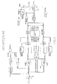
- FIG. 5 A block diagram of a preferred embodiment of the invention is depicted in Fig. 5, while the main signals are depicted in Fig. 6.
- the two independent arrays of sense amplifiers SENSE_EVEN, SENSE_ODD of the two memory banks are enabled at the same time by the pulse UPDATE, but only the sense amplifiers of memory bank in state of priority, identified by the logic value of the least significant bit A0 of the address, can place the read data on the internal data bus.
- the block CONTROL_LOGIC if the first bank in priority is the ODD bank generates a first increment pulse for the counter EVEN on the relative bank EVEN of which the read cycle pertaining to the next successive address takes place.
- the same increment signal for the bank that is not in priority stimulates the respective circuit SENSE CTRL TIMING managing the sense amplifiers SENSE_EVEN, SENSE_ODD.
- the array of sense amplifiers, the managing circuit SENSE CTRL TIMING, the dummy equalization structures etc. will process the increment pulse as a normal request of an asynchronous reading and will be restarted, while the sense amplifiers of the bank in priority, being independent from those of the other bank, will continue to evolve through the reading phase.
- the control circuit will continue to monitor the signals coming from the block SENSE CTRL TIMING of the bank in priority and, as soon as it generates the signal DLATCH for transferring the read datum to the latch in cascade of the sense amplifiers, it will produce the pulse LOAD for loading the read datum in the output latch.
- the falling (trailing) edge of the pulse LOAD establishes that the bank that has just terminated the reading is ready to start a new read cycle.
- a new increment signal will be produced only for the counter of this bank, that besides stimulating the generation of the new internal address, will restart the reading exclusively for this bank.
- control circuit shall wait for information coming from the external input bus or from the self-adapting structure of the SENSE CTRL TIMING to enable the outputting of data of the other bank, by way of the generation of a new pulse LOAD or to start a new asynchronous read cycle.
- the signal OEn (“Output Enable”) is a low-active external command for enabling the output buffers, thus if it assumes the logic level "0" the data of the bank in priority are transferred to the output buffers and made available to the external world from outside.
- the circuit for detecting address transitions TRANSITION_DETECTOR produces a detection pulse ATD_ADD starting from which the pulse signals that allow the comparison between the external address and the address stored in the address counters are generated.
- the address consecutive to the one of the last completed reading is present in the counter of the bank that is currently not in priority. If the external address is equal to this address, the relative datum can be output and a new reading on this bank may start again.
- the block TRANSITION_DETECTOR produces a pulse ATD_ADD, that is suitably delayed and stretched by the block DELAY&STRETCH.
- This block produces the signal COMPARE as a delayed and stretched version of the pulse ATD_ADD, in order to account for the processing time of the signal NEW_ADDR .
- the blocks SENSE CTRL TIMING may be similar to that described in the prior patent application EP-00830068.3 in the name of the same applicant, that is they are self-adaptive structures suitable to manage the timing of the read phases of sense amplifiers.
- the NEW_SYNC signal contains the information relative to the fact that the user requires a new datum and that the address in which it is stored is consecutive to the previous one. Therefore, if the reading relative to this new address is terminated, that is the sense amplifiers have already placed into the relative DATA_REGISTER latch the read datum, the datum is output and a new read cycle is started onto the same bank, after having incremented its address counter. If on the contrary the reading has not yet finished, the system waits for the end of the read cycle.
- the memory device of the invention if used always in an asynchronous mode, could be slightly less performing than a standard asynchronous memory device, because of the delay introduced in the phase that immediately follows the change of the external address in order to recognize the required read mode (synchronous or asynchronous).
- the block CHARGE_CONTROL generates a precharge signal PRECHARGE of the output node, setting it at the voltage Vcc/2 .
- the pulse ATD is obtained as a logic AND between the control pulses ATD_CEn and the address transition detection pulse ATD_ADD , and indicates that an address transition or a resume from a stand-by state has occurred.
- the precharge phase of the output node stops when the block CONTROL_LOGIC enables the output of the datum read by the sense amplifiers by way of the signals LOAD_EVEN and LOAD_ODD. This phase is further conditioned by the state of the signal DISABLE that sets in a high impedance state the outputs and that depends from the state of signals CEn and OEn.
- the path from the DATA_REGISTER to the output buffer is interrupted because the signal OUTLATCH is forced low by the NOR gate input with the above mentioned signals PRE_CHARGE and DISABLE.
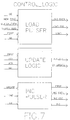
- the block CONTROL_LOGIC is constituted by three main circuits, as depicted in Fig. 7:
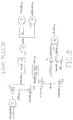
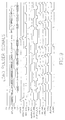
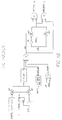
- FIG. 8 A block diagram of a possible embodiment of the circuit is depicted in Fig. 8, while Fig. 9 illustrates the temporal evolution of the main signals.
- Fig. 8 is depicted a block PULSER that produces a pulse of a certain duration each time it is stimulated by a transition 0 ⁇ 1 of the signal LOAD_STIM .
- the signal LOAD_STIM is the logic AND between the logic negation of the external enabling command of the output buffer OE and the signal DLATCH_E_On.
- the first signal ( OE ) contains the information relative to the enabling of the output buffer of the memory
- the second ( DLATCH_E_On ) contains the information that the reading in progress has ended and the respective data latches in cascade to the sense amplifiers SENSE_EVEN, SENSE_ODD have been updated.
- the block ONLY_FALLING_EDGE_DELAY delays only the falling edge of the start signal UPDATE of an asynchronous reading by producing the signal UPDATE_DEL .
- This signal is logically inverted and ANDed with the output of the pulse generator PULSER, and its function is to interrupt an eventual pulse LOAD when a new asynchronous reading starts.
- demultiplexer controlled by the state of A0 (constituted by the gates 13 and I4) directs the pulse LOAD towards the bank in priority.
- the circuit includes a pulse generator PULSER stimulated by a signal output by the multiplexer constituted by the two pass gates PG1, PG2. Said multiplexer is controlled by the signal FIRST that discriminates the first asynchronous read cycle from the successive synchronous ones.
- the signal FIRST is generated by a latch SR, set by the start signal UPDATE of the asynchronous reading and reset by the signal LOAD that enables the loading of the datum read from the sense amplifiers, thus stating the end of the first asynchronous read cycle.
- the pulse generator PULSER is stimulated by a replica of the signal UPDATE, delayed by the block CARRY_DELAY , in order to account for the propagation delay of the carry bit through the counter.
- PULSER is stimulated by the logic negation of the signal LOAD to allow, at the end of the pulse LOAD, the increment of the address counter and the start of a new reading on the bank that has just terminated the current read cycle.
- the pulse output by the pulse generator is logically filtered in the following situations:
- the block ONLY_FALLING_EDGE_DELAY delays only the falling edge of the signal UPDATE producing the signal UPDATE_DEL that, when it is at the high logic level, filters the increment.
- the pulse INC is correctly directed to the banks EVEN and ODD through the demultiplexer constituted by the AND gates I4 and I5 controlled by:
- a pulse ATD (after having been logically negated) sets Q1 to 1.
- Q1 will be reset to 0 only by a general increment pulse INC, as long as it is not the INC pulse that is produced during the first asynchronous reading to increment the bank EVEN when the first asynchronous reading starts on the bank ODD.
- Such an INC pulse is in fact filtered by the AND gate I5 by using the logic negation of the signal FIRST.
- the signal Q1 enables, at the end of the pulse ATD, to force to 1 the signal SET (I4) which in turn sets to 1 the output WAIT of the LATCH L2.
- the signal WAIT when at high logic level, carries the information that a first pulse ATD has been detected. Therefore, a successive pulse ATDn arriving in this phase produces, through I2, a pulse START_UPDATE , that in turn produces a restart signal OK_UPDATE of an asynchronous d cycle.
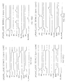
- Fig. 13c highlights a possible time evolution of the signals in the case of a standard synchronous reading phase
- Fig. 13d illustrates the situation in which the new pulse ATD follows a previous one without being preceded by a general increment pulse INC, thus causing the generation of the pulse OK_UPDATE .
Landscapes
- Dram (AREA)
Abstract
Description
- simultaneous readings and multiplexing of the outputs;
- time outphased readings.
- If A0=0:
- the first read datum is relative to the address X of the bank EVEN and the successive read datum is the datum X of the bank ODD.
- If A0=1:
- the first read datum is relative to the address X of the bank ODD and the successively read datum is relative to the X+1 address of the bank EVEN.
- presence of a further pin for the additional control signal ALE, that is necessary to catch all external addresses in case of asynchronous access;
- incompatibility with standard memory devices in which this further pin is not expected;
- specific protocol that uses the signal OEn as a clock signal for synchronous reading;
- need of the user of redesigning the software and the hardware of the system.
- Current address consecutive to the previous one;
- Current address not consecutive to the previous one.
- resume from stand-by state;
- loss of synchronism due to excessively fast address changes (out of specifications).
- a load circuit, LOAD_PULSER, that produces pulses for loading a read datum in the output register;
- a generator INC_PULSER of increment pulses for the address counters and for starting new read cycles in the two banks;
- a restart circuit UPDATE_LOGIC, that recognizes anomalous conditions in which an asynchronous read cycle must restart and generates the signals ATD_CEn and OK_UPDATE.
- it produces the pulses necessary for loading the read datum in the latch that precedes the output buffer;
- during the first asynchronous reading it is stimulated by the signal DLATCH to produce the first load pulse LOAD;
- in the successive synchronous readings it is stimulated by the switching of the external address monitored by way of the signal NEW_SYNC;
- it is able to synchronize the user request of a new datum with its availability;
- depending on the address A0, it allows the loading of the datum EVEN or of the datum ODD.
- producing the pulses that are necessary to increment the addresses stored in the address counters of the two banks and starting asynchronous readings;
- producing the first increment considering the propagation delay of the carry through the counter;
- suppressing the first increment if the asynchronous reading starts from an address on the EVEN bank;
- producing at the end of the respective read cycles the next increments for each of the two banks;
- producing a signal FIRST capable to discriminate the first asynchronous reading from the successive synchronous readings;
- updating the pointer to the banks EVEN and ODD, in function of the address A0.
- in case of a first asynchronous reading EVEN (A0=0 and FIRST=1), during which, as already stated, it is not necessary to increase the ODD bank because its address counter already contains the correct address: in this situation OK_INC=0;
- in case of eventual increments being in progress at the start of a new asynchronous reading cycle (UPDATE=1) that update the content of the counters with the new external address.
- the signal A0 when FIRST=0. In this case the increment is provided to the bank in priority that has just made available the read datum;
- the logic negation of the signal A0 when FIRST=1. In this case the increment is provided to the bank that is not in priority: in fact, if the first asynchronous reading starts on the bank ODD, the first increment pulse must be provided to the counter EVEN.
Claims (7)
- An interleaved memory readable in sequential access synchronous mode and in random access asynchronous mode, having two banks of memory cells (EVEN_MATRIX, ODD_MATRIX) each provided with an internal address counter (EVEN_COUNTER, ODD_COUNTER), decoding structures and sensing circuitry (EVEN_SIDE, ODD_SIDE, SENSE_EVEN, SENSE_ODD, SENSE CTRL TIMING), input address buffers (INPUT_BUFFERS), control signal buffers and output data buffers (BUFOUT), a control circuit (CONTROL_LOGIC) receiving external commands of enabling of the memory (CEn), of enabling of the output buffers (OEn) and at least an address transition detection signal (COMPARE) produced by means of a detecting circuit (TRANSITION_DETECTOR), characterized in thatsaid detecting circuit (TRANSITION_DETECTOR) produces a detection pulse (ATD_ADD) upon a change of the address input from outside in said address buffers (INPUT_BUFFERS);a delay circuit (DELAY&STRETCH) produces the detection signal (COMPARE) by delaying and stretching the active phase of said detection pulse (ATD_ADD);said decoding and sensing structures of the two banks are functionally independent from each other;an internal data bus for transferring data stored in latches of the respective array of sense amplifiers of one or the other bank (SENSE_EVEN, SENSE_ODD, SENSE CTRL TIMING) to a data register (DATA_EV_REGISTER, DATA_ODD_REGISTER) and from said data register (DATA_EV_REGISTER, DATA_ODD_REGISTER) to an array of output buffers (BUFOUT) under control of a load signal (LOAD_EVEN, LOAD_ODD) specific for one and the other bank generated by said control circuit (CONTROL_LOGIC);said control circuit (CONTROL_LOGIC) discriminating the requested access and reading mode, depending on a synchronous read stimulation signal (NEW_SYNC) and of an asynchronous read start signal (UPDATE) internally generated, among which the first is active when a new external address coincides with one of addresses stored in said address counters (EVEN_COUNTER, ODD_COUNTER) upon the enabling of said detection signal (COMPARE), the second assumes a certain logic state (UPDATE=1) when an input external address differs from the addresses stored in said address counters (EVEN_COUNTER, ODD_COUNTER) upon the activation of said detection signal (COMPARE);a transition to said high logic state of said asynchronous read start signal (UPDATE 0→1), enabling the acquisition of an input address in said counters (EVEN_COUNTER, ODD_COUNTER), the start of a new random access asynchronous read cycle with a simultaneous activation of the sense amplifier arrays (EVEN_SIDE, ODD_SIDE) and of respective sensing circuitry (SENSE CTRL TIMING) of both banks, said command of enabling the output buffers (OEn) acting as an enabling signal for transferring the data read from the bank (EVEN_MATRIX, ODD_MATRIX) currently in priority, established by the value of the least significant bit (A0) of the input address, in the respective output buffer of the bank;return of said asynchronous read start signal (UPDATE) to the other logic state (UPDATE→0) causing after a certain delay the switching to a sequential (burst) access synchronous read mode by generating or not, within said control circuit (CONTROL_LOGIC), a first increment pulse (INC_EVEN) for the counter of internal addresses of the bank currently not in priority (EVEN_MATRIX), implementing or not an outphasing between the two banks from the first synchronous mode read cycle depending on the value assumed by said least significant bit (A0), progressing under control of said read stimulation signal (NEW_SYNC) and of a third command (LOAD_EVEN, LOAD_ODD) for loading the data in the output buffers (BUFOUT), internally generated in the control circuit (LOAD PULSER), the sequential reading of stored data.
- The interleaved memory of claim 1, wherein said asynchronous read start signal (UPDATE) assumes said logic state (UPDATE=1) even when a restart signal of asynchronous reading (OK_UPDATE) produced by said control circuit (CONTROL_LOGIC) is active.
- The interleaved memory of claim 2, wherein said control circuit (CONTROL_LOGIC) comprisesa circuit (INC_PULSER) generating said increment pulses (INC_EVEN; INC_ODD) for the counters of the internal addresses of said banks of memory cells, stimulated by said asynchronous read start signal (UPDATE) during a first asynchronous reading and by a load pulse (LOAD) during synchronous readings successive to said first asynchronous read;a load circuit (LOAD_PULSER) producing said load commands (LOAD_EVEN, LOAD_ODD) equal to a load pulse (LOAD) respectively depending on the fact that the least significant address bit (A0) identifying one of said banks of memory cells assumes a certain logic state (A0=0) or the other logic state (A0=1), said load pulse (LOAD) being produced in function of said asynchronous read signal and of transfer signals (DLATCH_EVEN, DLATCH_ODD) of a datum read from the banks of memory cells (EVEN_MATRIX, ODD_MATRIX) in respective data registers (DATA_EV_REGISTER, DATA_ODD_REGISTER);a restart circuit (UPDATE_LOGIC) producing said restart signal of asynchronous read (OK_UPDATE) when a change of address occurs before the end of a synchronous or asynchronous read cycle.
- The interleaved memory of claim 3, wherein said generating circuit (INC_PULSER) comprisesa latch SR, being set by the asynchronous read start signal (UPDATE) and being reset by a load pulse (LOAD), producing a signal (FIRST) discriminating an asynchronous read from a successive synchronous read,a multiplexer (PG1, PG2) controlled by said discriminating signal (FIRST) being input with a delayed replica of said asynchronous read start signal (UPDATE) and the logic negation of said load pulse (LOAD),a pulse generator (PULSER) in cascade to the multiplexer (PG1, PG2) producing a pulse of a pre-established duration when the output of said multiplexer (PG1, PG2) is enabled,a logic circuit producing a general increment pulse (INC) as logic AND between the pulse produced by said pulse generator (PULSER), the logic negation of a replica of said asynchronous read start signal (UPDATE) delayed on the transition edge (UPDATE 1→0) from said logic state to the other logic state and the logic OR between the memory address bit (A0) identifying one of the two banks of memory cells (EVEN_MATRIX, ODD_MATRIX) and the logic negation of said discriminating signal (FIRST),a second multiplexer (PG3, PG4)controlled by said discriminating signal (FIRST), being input with said address bit (A0) and its logic negation,a logic circuit producing said increment pulse (INC_EVEN, INC_ODD) respectively as logic AND between said general increment pulse (INC) and the logic negation of the output of said second multiplexer (PG3, PG4), and as logic AND between said general increment pulse (INC) and the output of said second multiplexer (PG3, PG4).
- The interleaved memory according to claim 4, wherein said restart circuit (UPDATE_LOGIC) comprises a pulse generator (FALLING_EDGE_TRANSITION_DETECTOR) producing a control pulse (ATD_CEn) upon the activation of said external commands of enabling of the memory (CEn),a latch SR being set by the logic negation (ATDn) of a second detection signal (ATD) obtained as logic AND between said control pulse (ATD_CEn) and said detection pulse (ATD_ADD), and being reset by a reset signal (INC_RES) obtained as logic AND between the general increment pulse (INC) and the logic negation of the discriminating signal (FIRST),another latch SR being set by the logic AND (SET) of the true output (Q) of said first latch SR and of said second detecting signal (ATD), and being reset by the logic NOR (RESET) of the true output (Q) of said first latch SR and of said reset signal (INC_RES),a logic circuit producing said restart signal of asynchronous read (OK_UPDATE) as logic OR between the logic negation of said control pulse (ATD_CEn) and the logic AND between the true output (Q) of said other latch SR and the logic negation (ATDn) of the second detection signal.
- The interlace memory according to one of claims 4 and 5, wherein said load circuit (LOAD_PULSER) producing said load commands (LOAD_EVEN, LOAD_ODD) equal to a load pulse (LOAD) respectively depending on the fact that the address bit (A0) identifying one of said banks of memory cells assumes a certain logic state (A0=0) or the other logic state (A0=1), comprisinga multiplexer controlled by said address bit (A0) being input with a pair of transfer signals (DLATCH_EVEN, DLATCH_ODD) of a datum read from the banks of memory cells (EVEN_MATRIX, ODD_MATRIX) in respective data registers (DATA_EV_REGISTER, DATA_ODD_REGISTER),a latch SR being set by said read stimulation signal (NEW_SYNC) and reset by said load pulse (LOAD) producing a synchronization signal (SYNC_OK),another multiplexer controlled by said discriminating signal (FIRST) being input with a pair of logic signals constituted by the logic AND between the logic negation of said command of enabling of the output buffers (OE) and the logic negation of the output of said first multiplexer, and by the logic AND between the logic negation of the command of enabling of the output buffers (OE), the logic negation of the output of said first multiplexer and said synchronization signal (SYNC_OK),a pulse generator (PULSER) in cascade to the other multiplexer producing a pulse of a pre-established duration upon the activation of said other multiplexer,a logic circuit producing said load pulse (LOAD) as logic AND between the pulse produced by said pulse generator (PULSER) and the logic negation of a replica of said asynchronous read start signal (UPDATE) delayed on the transition edge (UPDATE 1→0) from said logic state to the other,another logic circuit producing said load commands (LOAD_ODD, LOAD_EVEN) respectively as logic AND between said address bit (A0) and said load pulse (LOAD) and as logic AND between the logic negation of said address bit (A0) and said load pulse (LOAD).
- The memory according to one of claims from 1 to 6 wherein said output buffer (BUFOUT) comprises precharge means of the output node to an intermediate voltage between the voltages corresponding to two different logic states of an output datum.
Priority Applications (3)
| Application Number | Priority Date | Filing Date | Title |
|---|---|---|---|
| DE60041263T DE60041263D1 (en) | 2000-10-18 | 2000-10-18 | Nested memory device with random and sequential access |
| EP00830675A EP1199723B1 (en) | 2000-10-18 | 2000-10-18 | Interlaced memory device with random or sequential access |
| US09/977,561 US6701419B2 (en) | 2000-10-18 | 2001-10-15 | Interlaced memory device with random or sequential access |
Applications Claiming Priority (1)
| Application Number | Priority Date | Filing Date | Title |
|---|---|---|---|
| EP00830675A EP1199723B1 (en) | 2000-10-18 | 2000-10-18 | Interlaced memory device with random or sequential access |
Publications (2)
| Publication Number | Publication Date |
|---|---|
| EP1199723A1 true EP1199723A1 (en) | 2002-04-24 |
| EP1199723B1 EP1199723B1 (en) | 2008-12-31 |
Family
ID=8175514
Family Applications (1)
| Application Number | Title | Priority Date | Filing Date |
|---|---|---|---|
| EP00830675A Expired - Lifetime EP1199723B1 (en) | 2000-10-18 | 2000-10-18 | Interlaced memory device with random or sequential access |
Country Status (3)
| Country | Link |
|---|---|
| US (1) | US6701419B2 (en) |
| EP (1) | EP1199723B1 (en) |
| DE (1) | DE60041263D1 (en) |
Cited By (1)
| Publication number | Priority date | Publication date | Assignee | Title |
|---|---|---|---|---|
| EP1788575A1 (en) * | 2005-11-18 | 2007-05-23 | STMicroelectronics S.r.l. | Method for accessing in reading, writing and programming to a NAND non-volatile memory electronic device monolithically integrated on semiconductor |
Families Citing this family (28)
| Publication number | Priority date | Publication date | Assignee | Title |
|---|---|---|---|---|
| US6782459B1 (en) * | 2000-08-14 | 2004-08-24 | Rambus, Inc. | Method and apparatus for controlling a read valid window of a synchronous memory device |
| US6690606B2 (en) * | 2002-03-19 | 2004-02-10 | Micron Technology, Inc. | Asynchronous interface circuit and method for a pseudo-static memory device |
| DE60235888D1 (en) * | 2002-09-12 | 2010-05-20 | St Microelectronics Asia | Pseudo-two-dimensional random access memory |
| US6920524B2 (en) | 2003-02-03 | 2005-07-19 | Micron Technology, Inc. | Detection circuit for mixed asynchronous and synchronous memory operation |
| US7225306B2 (en) * | 2004-06-23 | 2007-05-29 | Texas Instruments Incorporated | Efficient address generation for Forney's modular periodic interleavers |
| US7327803B2 (en) | 2004-10-22 | 2008-02-05 | Parkervision, Inc. | Systems and methods for vector power amplification |
| US7355470B2 (en) | 2006-04-24 | 2008-04-08 | Parkervision, Inc. | Systems and methods of RF power transmission, modulation, and amplification, including embodiments for amplifier class transitioning |
| US7457993B2 (en) * | 2004-11-16 | 2008-11-25 | Texas Instruments Incorporated | Error free dynamic rate change in a digital subscriber line DSL with constant delay |
| US7560956B2 (en) * | 2005-08-03 | 2009-07-14 | Micron Technology, Inc. | Method and apparatus for selecting an operating mode based on a determination of the availability of internal clock signals |
| US8334722B2 (en) | 2007-06-28 | 2012-12-18 | Parkervision, Inc. | Systems and methods of RF power transmission, modulation and amplification |
| US7911272B2 (en) | 2007-06-19 | 2011-03-22 | Parkervision, Inc. | Systems and methods of RF power transmission, modulation, and amplification, including blended control embodiments |
| US8013675B2 (en) | 2007-06-19 | 2011-09-06 | Parkervision, Inc. | Combiner-less multiple input single output (MISO) amplification with blended control |
| US8031804B2 (en) | 2006-04-24 | 2011-10-04 | Parkervision, Inc. | Systems and methods of RF tower transmission, modulation, and amplification, including embodiments for compensating for waveform distortion |
| US7937106B2 (en) | 2006-04-24 | 2011-05-03 | ParkerVision, Inc, | Systems and methods of RF power transmission, modulation, and amplification, including architectural embodiments of same |
| US8315336B2 (en) | 2007-05-18 | 2012-11-20 | Parkervision, Inc. | Systems and methods of RF power transmission, modulation, and amplification, including a switching stage embodiment |
| KR20090102789A (en) * | 2006-12-06 | 2009-09-30 | 퓨전 멀티시스템즈, 인크.(디비에이 퓨전-아이오) | Apparatus, system, and method for data storage using progressive raid |
| US7620129B2 (en) | 2007-01-16 | 2009-11-17 | Parkervision, Inc. | RF power transmission, modulation, and amplification, including embodiments for generating vector modulation control signals |
| US7983099B2 (en) | 2007-12-20 | 2011-07-19 | Mosaid Technologies Incorporated | Dual function compatible non-volatile memory device |
| US8307180B2 (en) | 2008-02-28 | 2012-11-06 | Nokia Corporation | Extended utilization area for a memory device |
| WO2009145887A1 (en) | 2008-05-27 | 2009-12-03 | Parkervision, Inc. | Systems and methods of rf power transmission, modulation, and amplification |
| US8874824B2 (en) | 2009-06-04 | 2014-10-28 | Memory Technologies, LLC | Apparatus and method to share host system RAM with mass storage memory RAM |
| KR20140026458A (en) | 2011-04-08 | 2014-03-05 | 파커비전, 인크. | Systems and methods of rf power transmission, modulation, and amplification |
| JP6174574B2 (en) | 2011-06-02 | 2017-08-02 | パーカーヴィジョン インコーポレイテッド | Antenna control |
| WO2013098463A1 (en) | 2011-12-29 | 2013-07-04 | Nokia Corporation | Method for erasing data entity in memory module |
| US9311226B2 (en) | 2012-04-20 | 2016-04-12 | Memory Technologies Llc | Managing operational state data of a memory module using host memory in association with state change |
| EP3047348B1 (en) | 2013-09-17 | 2025-03-19 | Parkervision, Inc. | Method for rendering an information bearing function of time |
| US9766823B2 (en) | 2013-12-12 | 2017-09-19 | Memory Technologies Llc | Channel optimized storage modules |
| CN114338806B (en) * | 2022-02-28 | 2022-06-21 | 湖南云畅网络科技有限公司 | Synchronous message processing method and system |
Citations (6)
| Publication number | Priority date | Publication date | Assignee | Title |
|---|---|---|---|---|
| EP0473311A2 (en) * | 1990-08-31 | 1992-03-04 | International Business Machines Corporation | Memory row redrive |
| US5691955A (en) * | 1995-09-05 | 1997-11-25 | Mitsubishi Denki Kabushiki Kaisha | Synchronous semiconductor memory device operating in synchronization with external clock signal |
| EP1017059A1 (en) | 1998-12-30 | 2000-07-05 | STMicroelectronics S.r.l. | Method for reading a memory, particularly a non-volatile memory |
| EP1020868A1 (en) * | 1997-02-17 | 2000-07-19 | Hitachi, Ltd. | Semiconductor integrated circuit device |
| EP1122734A1 (en) | 2000-01-31 | 2001-08-08 | STMicroelectronics S.r.l. | Burst interleaved memory with burst mode access in synchronous read phases wherein the two sub-arrays are independently readable with random access during asynchronous read phases |
| IT1313853B1 (en) | 1999-11-26 | 2002-09-24 | St Microelectronics Srl | SYNCHRONOUS OUTPUT BUFFER, ESPECIALLY FOR NON-VOLATILE MEMORIES. |
Family Cites Families (6)
| Publication number | Priority date | Publication date | Assignee | Title |
|---|---|---|---|---|
| US5339395A (en) * | 1992-09-17 | 1994-08-16 | Delco Electronics Corporation | Interface circuit for interfacing a peripheral device with a microprocessor operating in either a synchronous or an asynchronous mode |
| JP2704113B2 (en) * | 1994-04-26 | 1998-01-26 | 日本電気アイシーマイコンシステム株式会社 | Data processing device |
| EP1122735B1 (en) * | 2000-01-31 | 2010-09-01 | STMicroelectronics Srl | Interleaved data path and output management architecture for an interleaved memory and load pulser circuit for outputting the read data |
| EP1122733A1 (en) * | 2000-01-31 | 2001-08-08 | STMicroelectronics S.r.l. | Internal regeneration of the address latch enable (ALE) signal of a protocol of management of a burst interleaved memory and relative circuit |
| EP1122737A1 (en) * | 2000-01-31 | 2001-08-08 | STMicroelectronics S.r.l. | Circuit for managing the transfer of data streams from a plurality of sources within a system |
| EP1122739A3 (en) * | 2000-01-31 | 2003-12-17 | STMicroelectronics S.r.l. | Accelerated carry generation. |
-
2000
- 2000-10-18 EP EP00830675A patent/EP1199723B1/en not_active Expired - Lifetime
- 2000-10-18 DE DE60041263T patent/DE60041263D1/en not_active Expired - Lifetime
-
2001
- 2001-10-15 US US09/977,561 patent/US6701419B2/en not_active Expired - Lifetime
Patent Citations (6)
| Publication number | Priority date | Publication date | Assignee | Title |
|---|---|---|---|---|
| EP0473311A2 (en) * | 1990-08-31 | 1992-03-04 | International Business Machines Corporation | Memory row redrive |
| US5691955A (en) * | 1995-09-05 | 1997-11-25 | Mitsubishi Denki Kabushiki Kaisha | Synchronous semiconductor memory device operating in synchronization with external clock signal |
| EP1020868A1 (en) * | 1997-02-17 | 2000-07-19 | Hitachi, Ltd. | Semiconductor integrated circuit device |
| EP1017059A1 (en) | 1998-12-30 | 2000-07-05 | STMicroelectronics S.r.l. | Method for reading a memory, particularly a non-volatile memory |
| IT1313853B1 (en) | 1999-11-26 | 2002-09-24 | St Microelectronics Srl | SYNCHRONOUS OUTPUT BUFFER, ESPECIALLY FOR NON-VOLATILE MEMORIES. |
| EP1122734A1 (en) | 2000-01-31 | 2001-08-08 | STMicroelectronics S.r.l. | Burst interleaved memory with burst mode access in synchronous read phases wherein the two sub-arrays are independently readable with random access during asynchronous read phases |
Cited By (2)
| Publication number | Priority date | Publication date | Assignee | Title |
|---|---|---|---|---|
| EP1788575A1 (en) * | 2005-11-18 | 2007-05-23 | STMicroelectronics S.r.l. | Method for accessing in reading, writing and programming to a NAND non-volatile memory electronic device monolithically integrated on semiconductor |
| US7529881B2 (en) | 2005-11-18 | 2009-05-05 | Luigi Pascucci | Method for accessing in reading, writing and programming to a nand non-volatile memory electronic device monolithically integrated on semiconductor |
Also Published As
| Publication number | Publication date |
|---|---|
| EP1199723B1 (en) | 2008-12-31 |
| DE60041263D1 (en) | 2009-02-12 |
| US6701419B2 (en) | 2004-03-02 |
| US20020087817A1 (en) | 2002-07-04 |
Similar Documents
| Publication | Publication Date | Title |
|---|---|---|
| EP1199723B1 (en) | Interlaced memory device with random or sequential access | |
| EP1122734B1 (en) | Burst interleaved memory with burst mode access in synchronous read phases wherein the two sub-arrays are independently readable with random access during asynchronous read phases | |
| US6279090B1 (en) | Method and apparatus for resynchronizing a plurality of clock signals used in latching respective digital signals applied to a packetized memory device | |
| US6338127B1 (en) | Method and apparatus for resynchronizing a plurality of clock signals used to latch respective digital signals, and memory device using same | |
| US6662304B2 (en) | Method and apparatus for bit-to-bit timing correction of a high speed memory bus | |
| EP0995196B1 (en) | Method and apparatus for adaptively adjusting the timing of a clock signal used to latch digital signals, and memory device using same | |
| US20040158785A1 (en) | Method and apparatus for generating expect data from a captured bit pattern, and memory device using same | |
| US6360292B1 (en) | Method and system for processing pipelined memory commands | |
| EP1122735B1 (en) | Interleaved data path and output management architecture for an interleaved memory and load pulser circuit for outputting the read data | |
| JPH11316706A (en) | Data high-speed transfer synchronization system and data high-speed transfer synchronization method | |
| CN104282325B (en) | With the multiple data rates memory for reading timing information | |
| US5959900A (en) | Synchronous semiconductor memory having a reduced number of registers | |
| US20030112688A1 (en) | Refresh control method of semiconductor memory device and semiconductor memory device comprising the same control method | |
| JP3941974B2 (en) | Data output buffer control method for synchronous memory | |
| US6188640B1 (en) | Data output circuits for semiconductor memory devices | |
| US20030151971A1 (en) | DDR memory and storage method | |
| US6487140B2 (en) | Circuit for managing the transfer of data streams from a plurality of sources within a system | |
| KR100389038B1 (en) | Synchronous sram device with late write function | |
| US6674666B2 (en) | Device and method for timing the reading of a nonvolatile memory with reduced switching noise | |
| US6356505B2 (en) | Internal regeneration of the address latch enable (ALE) signal of a protocol of management of a burst interleaved memory and related circuit | |
| US6804756B2 (en) | Synchronization circuit for read paths of an electronic memory | |
| JP2025505783A (en) | Datapath circuits and methods | |
| EP1122739A2 (en) | Accelerated carry generation. | |
| EP1122736B1 (en) | ATD generation in a synchronous memory | |
| JPH08335397A (en) | Semiconductor memory |
Legal Events
| Date | Code | Title | Description |
|---|---|---|---|
| PUAI | Public reference made under article 153(3) epc to a published international application that has entered the european phase |
Free format text: ORIGINAL CODE: 0009012 |
|
| AK | Designated contracting states |
Kind code of ref document: A1 Designated state(s): AT BE CH CY DE DK ES FI FR GB GR IE IT LI LU MC NL PT SE Kind code of ref document: A1 Designated state(s): DE FR GB IT |
|
| AX | Request for extension of the european patent |
Free format text: AL;LT;LV;MK;RO;SI |
|
| 17P | Request for examination filed |
Effective date: 20021001 |
|
| AKX | Designation fees paid |
Free format text: DE FR GB IT |
|
| 17Q | First examination report despatched |
Effective date: 20071023 |
|
| GRAP | Despatch of communication of intention to grant a patent |
Free format text: ORIGINAL CODE: EPIDOSNIGR1 |
|
| GRAS | Grant fee paid |
Free format text: ORIGINAL CODE: EPIDOSNIGR3 |
|
| GRAS | Grant fee paid |
Free format text: ORIGINAL CODE: EPIDOSNIGR3 |
|
| GRAA | (expected) grant |
Free format text: ORIGINAL CODE: 0009210 |
|
| AK | Designated contracting states |
Kind code of ref document: B1 Designated state(s): DE FR GB IT |
|
| REG | Reference to a national code |
Ref country code: GB Ref legal event code: FG4D |
|
| REF | Corresponds to: |
Ref document number: 60041263 Country of ref document: DE Date of ref document: 20090212 Kind code of ref document: P |
|
| PLBE | No opposition filed within time limit |
Free format text: ORIGINAL CODE: 0009261 |
|
| STAA | Information on the status of an ep patent application or granted ep patent |
Free format text: STATUS: NO OPPOSITION FILED WITHIN TIME LIMIT |
|
| 26N | No opposition filed |
Effective date: 20091001 |
|
| REG | Reference to a national code |
Ref country code: FR Ref legal event code: ST Effective date: 20100630 |
|
| PG25 | Lapsed in a contracting state [announced via postgrant information from national office to epo] |
Ref country code: FR Free format text: LAPSE BECAUSE OF NON-PAYMENT OF DUE FEES Effective date: 20091102 |
|
| PG25 | Lapsed in a contracting state [announced via postgrant information from national office to epo] |
Ref country code: GB Free format text: LAPSE BECAUSE OF NON-PAYMENT OF DUE FEES Effective date: 20091018 |
|
| PG25 | Lapsed in a contracting state [announced via postgrant information from national office to epo] |
Ref country code: IT Free format text: LAPSE BECAUSE OF FAILURE TO SUBMIT A TRANSLATION OF THE DESCRIPTION OR TO PAY THE FEE WITHIN THE PRESCRIBED TIME-LIMIT Effective date: 20081231 |
|
| PGFP | Annual fee paid to national office [announced via postgrant information from national office to epo] |
Ref country code: DE Payment date: 20191227 Year of fee payment: 20 |
|
| REG | Reference to a national code |
Ref country code: DE Ref legal event code: R071 Ref document number: 60041263 Country of ref document: DE |