EP1199381A2 - Cutting Tool - Google Patents
Cutting Tool Download PDFInfo
- Publication number
- EP1199381A2 EP1199381A2 EP01308923A EP01308923A EP1199381A2 EP 1199381 A2 EP1199381 A2 EP 1199381A2 EP 01308923 A EP01308923 A EP 01308923A EP 01308923 A EP01308923 A EP 01308923A EP 1199381 A2 EP1199381 A2 EP 1199381A2
- Authority
- EP
- European Patent Office
- Prior art keywords
- coating layer
- nitride
- titanium carbide
- titanium
- nitride coating
- Prior art date
- Legal status (The legal status is an assumption and is not a legal conclusion. Google has not performed a legal analysis and makes no representation as to the accuracy of the status listed.)
- Withdrawn
Links
Images







Classifications
-
- B—PERFORMING OPERATIONS; TRANSPORTING
- B23—MACHINE TOOLS; METAL-WORKING NOT OTHERWISE PROVIDED FOR
- B23B—TURNING; BORING
- B23B27/00—Tools for turning or boring machines; Tools of a similar kind in general; Accessories therefor
- B23B27/14—Cutting tools of which the bits or tips or cutting inserts are of special material
-
- C—CHEMISTRY; METALLURGY
- C23—COATING METALLIC MATERIAL; COATING MATERIAL WITH METALLIC MATERIAL; CHEMICAL SURFACE TREATMENT; DIFFUSION TREATMENT OF METALLIC MATERIAL; COATING BY VACUUM EVAPORATION, BY SPUTTERING, BY ION IMPLANTATION OR BY CHEMICAL VAPOUR DEPOSITION, IN GENERAL; INHIBITING CORROSION OF METALLIC MATERIAL OR INCRUSTATION IN GENERAL
- C23C—COATING METALLIC MATERIAL; COATING MATERIAL WITH METALLIC MATERIAL; SURFACE TREATMENT OF METALLIC MATERIAL BY DIFFUSION INTO THE SURFACE, BY CHEMICAL CONVERSION OR SUBSTITUTION; COATING BY VACUUM EVAPORATION, BY SPUTTERING, BY ION IMPLANTATION OR BY CHEMICAL VAPOUR DEPOSITION, IN GENERAL
- C23C30/00—Coating with metallic material characterised only by the composition of the metallic material, i.e. not characterised by the coating process
- C23C30/005—Coating with metallic material characterised only by the composition of the metallic material, i.e. not characterised by the coating process on hard metal substrates
-
- Y—GENERAL TAGGING OF NEW TECHNOLOGICAL DEVELOPMENTS; GENERAL TAGGING OF CROSS-SECTIONAL TECHNOLOGIES SPANNING OVER SEVERAL SECTIONS OF THE IPC; TECHNICAL SUBJECTS COVERED BY FORMER USPC CROSS-REFERENCE ART COLLECTIONS [XRACs] AND DIGESTS
- Y10—TECHNICAL SUBJECTS COVERED BY FORMER USPC
- Y10T—TECHNICAL SUBJECTS COVERED BY FORMER US CLASSIFICATION
- Y10T407/00—Cutters, for shaping
- Y10T407/23—Cutters, for shaping including tool having plural alternatively usable cutting edges
- Y10T407/235—Cutters, for shaping including tool having plural alternatively usable cutting edges with integral chip breaker, guide or deflector
-
- Y—GENERAL TAGGING OF NEW TECHNOLOGICAL DEVELOPMENTS; GENERAL TAGGING OF CROSS-SECTIONAL TECHNOLOGIES SPANNING OVER SEVERAL SECTIONS OF THE IPC; TECHNICAL SUBJECTS COVERED BY FORMER USPC CROSS-REFERENCE ART COLLECTIONS [XRACs] AND DIGESTS
- Y10—TECHNICAL SUBJECTS COVERED BY FORMER USPC
- Y10T—TECHNICAL SUBJECTS COVERED BY FORMER US CLASSIFICATION
- Y10T407/00—Cutters, for shaping
- Y10T407/27—Cutters, for shaping comprising tool of specific chemical composition
Definitions
- the present invention relates to a cutting tool in which a tool body is made of ceramic and which is used as a throwaway chip, an end mill, a drill or the like. More specifically, it relates to a cutting tool in which surface coating is applied to the tool body made of ceramic for improving wear resistance.
- the coating layers are constructed of materials different in thermal expansion coefficient in plural layers, a difference in thermal expansion coefficient between the layers can also be a cause of a residual stress.
- a ceramic tool can be excellent in wear resistance.
- peeling of the coating layers tends to occur in using the tool.
- Japanese Patent Laid-Open No. 212,183/1988 proposes a tool in which an aluminum oxide/nitride layer is formed on a surface of a substrate, another aluminum oxide/nitride layer, a titanium carbide layer, a titanium nitride layer and a titanium carbide/nitride layer are further formed thereon in this order and a titanium nitride layer is still further formed on the outermost layer.
- an improvement in adhesion of coating layers is not said to be satisfactory even in the tool of the foregoing documents.
- the invention aims to provide a ceramic cutting tool which can secure stable cutting performance over a long period of time even under cutting conditions of exerting a high load thermally and mechanically and which can be produced at low costs.
- the cutting tool of the invention is characterized in that
- the main point in the invention lies in how to suppress the decrease in breakage resistance in the ceramic cutting tool having the coating layer formed thereon while maintaining adhesion between the coating layer and the ceramic substrate.
- the present inventors have conducted various investigations. Consequently, it has been found that the breakage resistance is advantageously improved by adopting silicon nitride ceramic as a ceramic substrate and further especially titanium carbide/nitride as a material of a coating layer. And, they have further assiduously conducted investigations, and have consequently found that the titanium carbide/nitride coating layer is, as schematically shown in Fig.
- a columnar structure formed to have a structure made mainly of columnar crystal grains grown in the layer thickness direction (hereinafter referred to as a columnar structure) and when an average size of crystal grains observed on the surface of the titanium carbide/nitride coating layer (hereinafter simply referred to also as an average size of columnar crystal grains) is expressed by d and an average thickness of the titanium carbide/nitride coating layer by t, t is adjusted to between 0.5 and 3 ⁇ m and a d/t value to at least 0.1 and at most 0.5 whereby a residual stress of the coating layer is reduced and better breakage resistance is obtained.
- the d/t value is adjusted to 0.5 or less, whereby a residual stress in the coating layer is suppressed and breakage resistance of the tool can be greatly improved.
- the structure of the titanium carbide/nitride coating layer can be the columnar structure by the CVD film formation. In this case, however, the d/t value varies depending on the formation temperature of the titanium carbide/nitride coating layer. At the lower formation temperature, the growth of crystal grains in the inner direction of the coating layer surface is relatively suppressed with respect to the growth in the thickness direction of the coating layer.
- the d/t value tends to be decreased.
- the effect of suppressing the residual stress in which the breakage resistance of the tool is markedly improved becomes outstanding especially when the formation temperature of the titanium carbide/nitride coating layer is limited to such an extent that the d/t value reaches 0.5 or less. This makes it possible to effectively suppress the breakage or the like in using the tool while using the less costly composite ceramic.
- the average size d is the average value dj of all grains appearing on the surface.
- d/t exceeds 0.5, the effect of suppressing the residual stress becomes unsatisfactory, and the improvement in breakage resistance is not expected.
- d/t is less than 0.1, it means that the formation temperature of the titanium carbide/nitride coating layer is extremely decreased. A uniform titanium carbide/nitride coating layer is not obtained, or adhesion between the titanium carbide/nitride coating layer and the ceramic substrate is decreased, and peeling of a coating layer or the like tends to occur in using the tool. More preferably, d/t is 0.1 to 0.3.
- the level of the residual stress of the titanium carbide/nitride coating layer is also influenced by the thickness of the titanium carbide/nitride coating layer.
- the average thickness of the titanium carbide/nitride coating layer is set at 0.5 to 3 ⁇ m whereby the residual stress can effectively be suppressed to improve the breakage resistance of the tool.
- the wear resistance is unsatisfactory.
- it exceeds 3 ⁇ m the residual stress level is increased which results in impairing the breakage resistance.
- the titanium carbide/nitride coating layer is formed by CVD in the intermediate low formation temperature range of 750°C to 900°C.
- the formation temperature reaction temperature
- 900°C the residual stress of the titanium carbide/nitride coating layer becomes too high, and the breakage resistance of the tool is not satisfactorily secured.
- 750°C a chemical reaction for forming titanium carbide/nitride does not proceed satisfactorily, and a uniform titanium carbide/nitride coating layer is hardly obtained.
- the formation temperature of the titanium carbide/titanium coating layer is preferably 830°C to 880°C.
- a ceramic substrate in a predetermined shape is mounted in a reaction vessel, and while this is heated at the foregoing reaction temperature, starting gases are passed along with a carrier gas (for example, a hydrogen gas (H 2 )). While a substance of a coating layer is formed by the chemical reaction of the starting gases, it is laminated on the surface of the ceramic substrate.
- a carrier gas for example, a hydrogen gas (H 2 )
- a substance of a coating layer is formed by the chemical reaction of the starting gases, it is laminated on the surface of the ceramic substrate.
- a gas containing a titanium source component for example, titanium chloride such as titanium tetrachloride (TiCl 4 ) or the like
- a nitrogen source component for example, a nitrogen gas (N 2 ) or ammonia (NH 3 )
- a mixture obtained by further mixing the starting gases of the titanium nitride coating layer with a carbon source component can be used in the formation of the titanium carbide/nitride coating layer.
- a nitrogen-containing organic compound for example, CH 3 CN (acetonitrile)
- CH 3 CN acetonitrile
- the average size d of the columnar crystal grain is also increased in the order of d1 ⁇ d2 ⁇ d3.
- Titanium carbide/nitride constituting the titanium carbide/nitride coating layer is a solid solution of titanium carbide (general formula: TiC) and titanium nitride (general formula: TiN), and the general formula is TiC 1-x N x (hereinafter simply referred to also as TiCN).
- the X value can be set variously depending on a composition ratio of the nitrogen source component and the carbon source component in the starting gases. It is also possible to form a coating layer in which a composition ratio of a nitrogen source component and a carbon source component during the film formation is changed either continuously or stepwise and an X value is changed in the thickness direction either continuously or stepwise.
- a larger X value that is, an amount of a titanium nitride component is larger
- wear resistance of a coating layer is improved.
- a substrate of a titanium carbide/nitride coating layer is a substrate made of silicon nitride ceramic or a titanium nitride layer to be described later
- a larger X value that is, an amount of a titanium nitride component is larger
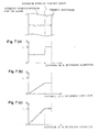
- a layer is formed while gradually increasing a ratio of an amount of a carbon source component to an amount of a nitrogen source component, whereby a coating layer of a gradient composition type in which X is larger on the side of the ceramic substrate and smaller on the side of the layer surface can be formed as shown in Fig. 7(b) or 7(c).
- the silicon nitride ceramic constituting the ceramic substrate is made mainly of silicon nitride (Si 3 N 4 ), and the remaining component is a sintering aid component.
- At least one type selected from an elemental group of Groups 3A, 4A, 5A, 3B (for example, Al (aluminum oxide or the like)) and 4B (for example, Si (silica or the like)) in the periodic table can be incorporated in the range of, for example, 5 % by mass or less, calculated as an oxide.
- These are present in the sintered product in the state of an oxide, a double oxide (for example, a metal silicate) or the like.
- the sintering aid component of Group 3A Sc, Y, La, Ce, Pr, Nd, Sm, Eu, Gd, Tb, Dy, Ho, Er, Tm, Yb and Lu are generally used.
- the content of these elements R is calculated as RO 2 in Ce only and as an R 2 O 3 -type oxide in others.
- an oxide of a heavy rare earth element such as Y, Tb, Dy, Ho, Er, Tm or Yb is preferably used because it is effective for improving strength, toughness and wear resistance of a silicon nitride sintered product.
- magnesia spinel, zirconium oxide and the like, other than this, are also available as a sintering aid.
- Silicon nitride as a constituent of the ceramic substrate has a considerably small thermal expansion coefficient in comparison with aluminum oxide (Al 2 O 3 ), titanium carbide (TiC), titanium nitride (TiN) or titanium carbide/nitride (typified by a composition of TiC 0.5 N 0.5 in the table) used as a constituent of the coating layer in the ceramic tool, and a residual stress tends to occur in the coating layer.
- Al 2 O 3 aluminum oxide
- TiC titanium carbide
- TiN titanium nitride
- titanium carbide/nitride typified by a composition of TiC 0.5 N 0.5 in the table
- the residual stress to the coating layer can greatly be suppressed by adopting the invention, it is possible to decrease the content of the sintering aid component in the silicon nitride ceramic to a lower value than an ordinary level, for example, preferably to less than 5 % by mass. Consequently, wear resistance of the ceramic substrate can be improved while maintaining breakage resistance of the tool. Nevertheless, for avoiding a disadvantage that the sintering of silicon nitride ceramic itself becomes difficult, it is preferable to add the sintering aid component in an amount of at least 1 % by mass.
- the structure of silicon nitride ceramic is that main phase crystal grains containing silicon nitride as a main component are bound through a vitreous and/or crystalline binding phase.
- the main phase is made mainly of an Si 3 N 4 phase in which a ⁇ -conversion rate is more than 70 % by volume (preferably more than 90 % by volume).
- the Si 3 N 4 phase may be a phase in which a part of Si's or N's is substituted with Al or oxygen or further a phase subjected to formation of a solid solution with a metal atom such as Li, Ca, Mg, Y or the like.
- main component (made mainly of", “mainly” or the like has the same meaning) means that in a substance in question, the content of its component is 50 % by mass or more, unless otherwise instructed.
- the sintering aid component mainly constitutes the binding phase, but a part thereof may be incorporated in the main phase.
- the binding phase sometimes contains, besides the component added on purpose as a sintering aid, unavoidable impurities such as silicon oxide contained in the silicon nitride starting powder and the like.
- a titanium nitride coating layer can be provided between the titanium carbide/nitride coating layer and the ceramic substrate (this titanium nitride layer can also be formed by the CVD film formation in the intermediate low temperature range). Since titanium nitride has better affinity for silicon nitride ceramic constituting the ceramic substrate than titanium carbonate/nitride, it is possible to increase adhesion of the overall coating layer by the insertion of the titanium nitride layer and to control the disadvantage such as peeling of the layer or the like more effectively. In this case, it is advisable that the average thickness of the titanium nitride layer inserted is adjusted to the range of 0.2 to 1 ⁇ m.
- Fig. 7(a) is an example in which the X value of titanium carbide/nitride constituting the titanium carbide/nitride coating layer is set at a nearly fixed value (0.5 herein) in the layer thickness direction.
- a solid line is an example in which X is continuously changed in the layer thickness direction, and a broken line is an example in which X is stepwise changed.
- Fig. 7(b) is an example in which the X value is, after gradually increased, finally maintained constantly at a value smaller than 1.
- the whole is a titanium carbide/nitride coating layer.
- the first layer in contact with the ceramic substrate is a titanium carbide/nitride layer in which the X value is nearly fixed in the thickness direction
- the second layer on the side of the layer surface is a titanium carbide/nitride layer of a gradient composition type in which the X value is changed in the layer thickness direction.
- the outside of the titanium carbide/nitride coating layer can optionally be coated with a titanium nitride coating layer (this titanium nitride coating layer can also be formed by the CVD film formation in the intermediate low temperature range). Since titanium nitride has a smaller friction coefficient than titanium carbide/nitride, wear resistance between the tool and a work to be cut can be reduced by coating with the titanium nitride coating layer. Even when heavy cutting or the like is conducted, it is possible to suppress the increase in the temperature of the edge. Consequently, a thermal shock due to addition of a temperature cycle can be lessened to further improve breakage resistance. Moreover, since heat generation is itself controlled, it can also contribute to improving wear resistance.
- the average thickness of such a titanium nitride coating layer is adjusted to the range of 0.3 to 1 ⁇ m.
- the average thickness is less than 0.3 ⁇ m, the effect of decreasing frictional resistance is at times not obtained satisfactorily.
- it exceeds 1 ⁇ m the effect of suppressing the residual stress is decreased, and the decrease in breakage resistance or the like tends to be invited.
- the "titanium carbide/nitride coating layer” attains the aim of the invention so long as it is made mainly of titanium carbide/nitride, and it may contain unavoidable impurities or a secondary component made of an intentional addition component unless the foregoing effects are impaired. Further, the “titanium nitride coating layer” also attains the aim of the invention so long as it is made mainly of titanium nitride, and it may contain unavoidable impurities or a secondary component made of an intentional addition component (provided a titanium carbide component in excess of an unavoidable impurity level (for example, 0.5 % by weight is an upper limit) is excluded) unless the foregoing effects are impaired.
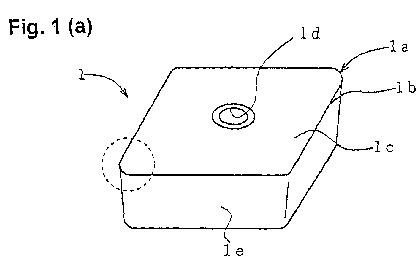
- Fig. 1 is a working example of a ceramic cutting tool in the invention, showing a throwaway chip 1 (hereinafter simply referred to also as a chip) constituting the tool body.
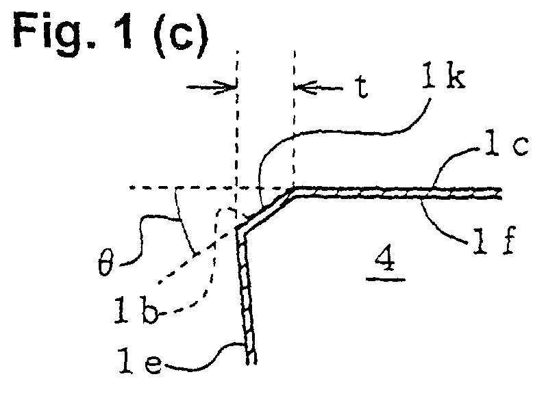
- the chip 1 has a structure that, as shown in Fig. 1(a), the entire outer surface of a ceramic substrate formed in a flat, nearly square block shape is coated with a coating layer 1f shown in Fig. 1(c).
- the main surface 1c forms a cutting face (hereinafter referred to also as a cutting face 1c), and the side surface 1e forms a flank (hereinafter referred to also as a flank 1e).
- each corner la is rounded as shown in Fig.
- a chamfer 1k is formed according to each cutting edge 1b as shown in Fig. 1(c). Further, as shown in Fig. 1(a), a penetration hole 1d for fitting the chip 1 to a chip holder not shown is formed through the center of the main surface 1c in the thickness direction.
- the chamber 1k has a flat section, and an angle ⁇ formed with the main surface 1c as the cutting face is adjusted to the range of, for example, 20 to 35°.
- the sectional shape of the chamber 1k can be an outwardly curved surface (rounded surface) as shown in Fig. 1(d) or a combination of a flat surface and a curved surface as shown in Fig. 1(e).
- the ceramic substrate 4 is made of silicon nitride ceramic, and the sintering aid component incorporated is, for example, 5 % by mass or less.
- the coating layer 1f is, for example, a titanium carbide/nitride coating layer as shown in Fig. 6.
- a silicon nitride powder and a sintering aid powder are mixed in predetermined amounts, a binder is added thereto for mixing as required, and the mixture is molded by a known method such as press molding (including a cold isostatic pressing method), injection molding or the like to form a molded article. Further, the molded article is sintered to obtain a ceramic substrate 4. Subsequently, the ceramic substrate 4 is installed in a reaction vessel, and this is heated in an intermediate low temperature range of 750°C to 900°C with a heater mounted within the reaction vessel.
- titanium carbide/nitride coating layer titanium tetrachloride and a gas as a carbon/nitrogen source (for example, acetonitrile or a mixed gas of nitrogen and hydrocarbon such as methane or the like) as starting gases are, in this state, passed through the reaction vessel along with hydrogen as a carrier gas. While titanium carbide/nitride is formed by the decomposition ⁇ reaction of the starting gases, it is laminated and grown on the surface of the ceramic substrate 4 to form the coating layer 1f.
- the reaction temperature is set at the foregoing range, whereby the d/t value of the coating layer 1f is adjusted to the range of 0.1 to 0.5.
- the absolute value of the thickness t at which to form the coating layer 1f is adjusted to the range of 0.5 to 3 ⁇ m according to the growth time.
- the chip 1 is used by being installed in the chip holder 11 for easy attaching and detaching as shown in Fig. 2. Specifically, the chip 1 and a sheet member 15 are overlaid with the chip 1 on an upper portion, and these are inserted into a concave installation part 12 formed in the tip of the chip holder 11. And, a screw 13 is penetrated into the penetration hole 1d (Fig. 1) of the chip 1 and a penetration hole (not shown) of the sheet member 15, and is screwed into the side of the chip holder 11, whereby the chip 1 is fastened in the chip holder 11 for easy attaching and detaching.
- Fig. 3 illustrates a face milling cutter 30 which is an example thereof.
- Plural cutting chips 32 are fixed in an outer peripheral surface of a rotary base 31.
- W indicates a work to be cut.
- Each of the cutting chips 32 is formed of the same material as the chip 1, and the same coating layer as in the chip 1 is formed on a cutting face 33 and a flank 34 which are adjacent relative to a cutting edge 35.
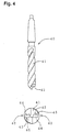
- Fig. 4 shows a drill 40 as another example.
- Two drill chips 42 are installed on a top surface of a shaft-like body 41.
- Each of the chips 42 is formed of the same material as the chip 1, and the same coating layer as in the chip 1 is formed on a cutting face 43 and a flank 44 which are adjacent relative to a cutting edge 45.
- an ⁇ -type silicon nitride powder (average particle diameter 0.5 ⁇ m, oxygen content 1.0 % by mass) was prepared as a starting powder, and an aluminum oxide powder, a magnesium oxide powder, a yttrium oxide powder, a ytterbium oxide powder and a zirconium oxide powder (average particle diameter of all these 1 ⁇ m or less) as sintering aid powders. And, these powders were mixed according to various compositions shown in Table 2, and wet-mixed and pulverized along with an alcohol as an organic solvent for 24 hours using a ball mill to obtain a starting slurry.
- the molded article was sintered in a nitrogen gas atmosphere at various temperatures for a period of time as shown in Table 2.
- a hot isostatic pressing (HIP) treatment was conducted, as required, at a temperature of 1600°C in a nitrogen gas atmosphere with a pressure of 150 MPa for 2 hours (whether the HIP treatment is conducted or not is shown in Table 2).
- the thus-obtained four sintered products were cut into the shape shown in Fig. 1 to form ceramic substrates 4.
- the thus-obtained four ceramic substrates 4 were placed in a reaction vessel of a known CVD device, and coating layers having the following conditions were formed in plural layers either singly or in combination to afford test chips.
- the film thickness of the coating layer formed is changed variously by adjusting the reaction time.
- MT means “moderate temperature” (or intermediate temperature)
- HT means “high temperature”. Therefore, for example, "MT-TiCN” means TiCN formed at a moderate temperature, and so forth.
- the coating layer(s) is (are) formed from the side of the ceramic substrate in the order described (incidentally, "Substrate No.” in the table refers to the number of the ceramic substrate used in Table 2).
- the structure of the coating layer after the formation was examined through X-ray diffraction. Consequently, it was found that the coating layers in (1) and (3) were made mainly of titanium carbide/nitride and the coating layer in (2) was made mainly of titanium nitride. Further, when the composition of the coating layer in (1) was examined by X-ray photoelectron spectroscopy, it was found to be TiC 0.3 N 0.7 .
- a rod-like work W to be cut was rotated around an axis, a test chip was contacted with its outer peripheral surface as shown in Fig. 9(b), and the outer peripheral surface of the work W to be cut was continuously dry-cut under the following cutting conditions using one main surface 1c as a cutting face and a side surface 1e as a flank:
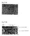
- Fig. 11 is SEM-observed images of a surface ((a)) and a broken surface ((b)) of the coating layer formed on test article (Example) No. 2 in Table 3.
- Fig. 12 is SEM-observed images of a surface ((a)) and a broken surface ((b)) of the coating layer formed on test article (Comparative Example) No. 13 in Table 3.
Landscapes
- Chemical & Material Sciences (AREA)
- Engineering & Computer Science (AREA)
- Mechanical Engineering (AREA)
- Chemical Kinetics & Catalysis (AREA)
- Materials Engineering (AREA)
- Metallurgy (AREA)
- Organic Chemistry (AREA)
- Cutting Tools, Boring Holders, And Turrets (AREA)
- Chemical Vapour Deposition (AREA)
Abstract


Description
| Material | Si3N4 | Al2O3 | TiC | TiCN | TiN |
| Thermal expansion coefficient (x 10/°C) | 3.2 | 8.5 | 7.6 | 8.4 | 9.2 |
β-sialon: Si6-zAlzOzN8-z (z = 0 to 4.2)
α-sialon: Mx(Si, Al)12(O,N)16 (x = 0 to 2)
M: Li, Mg, Ca, Y, R (R is a rare earth element except La and Ce).
By the way, in the invention, "main component" ("made mainly of", "mainly" or the like has the same meaning) means that in a substance in question, the content of its component is 50 % by mass or more, unless otherwise instructed.
| Sample No. | Composition (proportion by weight) | Sintering conditions | Theoretical density ratio (%) |
| 1 | MgO(1)-Y2O3(1) | 1900°C - 4Hr +HIP | 99.6 |
| 2 | MgO(0.5)-Al2O3(1)-Yb2O3(2) | 1850°C - 4Hr | 99.5 |
| 3 | MgO(1)-Y2O3(2)-ZrO2(1) | 1850°C - 4Hr | 99.8 |
| 4 | MgO(1.5)-Al2O3(1)-Y2O3(1.5)-ZrO2(2) | 1800°C - 4Hr | 99.8 |

| Cutting velocity V | 150 m/min; |
| Feed rate | 0.6 mm/l rotation; |
| Cutting amount | 2.0 mm; |
| Cutting oil | no (dry cutting); |
| Edge treatment | chamfer 0.1 mm x 25°; |
| Evaluation method | evaluation of breakage resistance with a processing distance until an edge is broken. |
Claims (8)
- A cutting tool comprising:wherein the titanium carbide/nitride coating layer has a structure made mainly of columnar crystal grains grown in the layer thickness direction, and when an average size of crystal grains observed on the surface of the titanium carbide/nitride coating layer is expressed by d and an average thickness of the titanium carbide/nitride coating layer by t, t is in the range of from 0.5 to 3 µm and the value of d/t is least 0.1 and at most 0.5.a tool body comprising a ceramic substrate made of silicon nitride ceramic, said substrate having a surface coated with a titanium carbide/nitride coating layer,
- A cutting tool according to claim 1, wherein the titanium carbide/nitride coating layer is formed by CVD in a temperature range of 750°C to 900°C.
- A cutting tool according to claim 1 or 2, wherein the total amount of a sintering aid component contained in the silicon nitride ceramic is 5 % by mass or less.
- A cutting tool according to any one of claims 1 to 3, wherein an intermediate titanium nitride coating layer is provided between the titanium carbide/nitride coating layer and the ceramic substrate.
- A cutting tool according to claim 4, wherein the average thickness of the titanium nitride coating layer is in the range of from 0.2 µm to 1 µm.
- A cutting tool according to any one of claims 1 to 5, wherein the exterior of the titanium carbide/nitride layer is coated with a titanium nitride coating layer.
- A cutting tool according to any one of claims 1 to 6, wherein the tool body is constructed as a throwaway chip.
- A cutting tool according to claim 7, comprising the throwaway chip and a chip holder in which the throwaway chip is installed, for easy attachment and detachment.
Applications Claiming Priority (2)
| Application Number | Priority Date | Filing Date | Title |
|---|---|---|---|
| JP2000318906 | 2000-10-19 | ||
| JP2000318906 | 2000-10-19 |
Publications (2)
| Publication Number | Publication Date |
|---|---|
| EP1199381A2 true EP1199381A2 (en) | 2002-04-24 |
| EP1199381A3 EP1199381A3 (en) | 2003-04-02 |
Family
ID=18797454
Family Applications (1)
| Application Number | Title | Priority Date | Filing Date |
|---|---|---|---|
| EP01308923A Withdrawn EP1199381A3 (en) | 2000-10-19 | 2001-10-19 | Cutting Tool |
Country Status (3)
| Country | Link |
|---|---|
| US (1) | US20020076284A1 (en) |
| EP (1) | EP1199381A3 (en) |
| KR (1) | KR20020033436A (en) |
Families Citing this family (12)
| Publication number | Priority date | Publication date | Assignee | Title |
|---|---|---|---|---|
| DE10243104A1 (en) * | 2002-09-17 | 2004-03-25 | Gebr. Brasseler Gmbh & Co. Kg | Rotating ceramic tool with a ceramic cutting head bonded to a ceramic or metal support shaft |
| US7581906B2 (en) * | 2004-05-19 | 2009-09-01 | Tdy Industries, Inc. | Al2O3 ceramic tools with diffusion bonding enhanced layer |
| JP4585243B2 (en) * | 2004-06-30 | 2010-11-24 | 株式会社アライドマテリアル | Single crystal diamond cutting tool for ultra-precision machining |
| US20080119349A1 (en) * | 2004-12-22 | 2008-05-22 | Ngk Spark Plug Co., Ltd. | Sialon Insert and Cutting Tool Equipped Therewith |
| SE530252C2 (en) * | 2006-12-27 | 2008-04-08 | Sandvik Intellectual Property | Ceramic silicon nitride material for use in cutting tool applications e.g. machining metals e.g. gray cast iron by e.g. chip forming machining method has predetermined amount of refractory hard phase e.g. titanium nitride |
| BR112012003880A2 (en) * | 2009-08-21 | 2016-03-29 | Ceramtec Gmbh | precision pressing and sintering of cutting boards, especially reversible cutting boards |
| US20130216777A1 (en) * | 2012-02-21 | 2013-08-22 | Wenping Jiang | Nanostructured Multi-Layer Coating on Carbides |
| CN105073310B (en) * | 2013-02-13 | 2017-03-08 | 京瓷株式会社 | Cutting element |
| KR102123996B1 (en) | 2013-02-25 | 2020-06-17 | 삼성전자주식회사 | Aluminum precursor, method of forming a thin layer and method of forming a capacitor using the same |
| US9764986B2 (en) | 2015-01-22 | 2017-09-19 | Kennametal Inc. | Low temperature CVD coatings and applications thereof |
| US10112200B2 (en) * | 2015-04-29 | 2018-10-30 | Spokane Industries | Composite milling component |
| WO2021145165A1 (en) * | 2020-01-17 | 2021-07-22 | 株式会社アライドマテリアル | Single-crystal diamond cutting tool |
Family Cites Families (5)
| Publication number | Priority date | Publication date | Assignee | Title |
|---|---|---|---|---|
| US4416670A (en) * | 1982-05-20 | 1983-11-22 | Gte Laboratories Incorporated | Carbide coated composite silicon nitride cutting tools |
| JPS58217477A (en) * | 1982-06-09 | 1983-12-17 | 住友電気工業株式会社 | Surface-coated ceramic throw-away chip |
| JPH0663804A (en) * | 1992-08-21 | 1994-03-08 | Mitsubishi Materials Corp | Throw-away tip for cutting made of silicon-nitride-based coated ceramics |
| US6221469B1 (en) * | 1998-12-09 | 2001-04-24 | Seco Tools Ab | Grade for steel |
| JP4558884B2 (en) * | 2000-03-31 | 2010-10-06 | 京セラ株式会社 | Drill throw-away tip and drill |
-
2001
- 2001-10-18 KR KR1020010064277A patent/KR20020033436A/en not_active Withdrawn
- 2001-10-18 US US09/978,801 patent/US20020076284A1/en not_active Abandoned
- 2001-10-19 EP EP01308923A patent/EP1199381A3/en not_active Withdrawn
Also Published As
| Publication number | Publication date |
|---|---|
| EP1199381A3 (en) | 2003-04-02 |
| KR20020033436A (en) | 2002-05-06 |
| US20020076284A1 (en) | 2002-06-20 |
Similar Documents
| Publication | Publication Date | Title |
|---|---|---|
| US5525134A (en) | Silicon nitride ceramic and cutting tool made thereof | |
| EP1188504B1 (en) | Coated cutting tool | |
| US7771847B2 (en) | cBN sintered body for high surface integrity machining, cBN sintered body cutting tool, and cutting method using the same | |
| KR101412164B1 (en) | Cloth cutting tool and manufacturing method thereof | |
| US20020076284A1 (en) | Cutting tool | |
| US6824727B2 (en) | Method for preparing SiAlON ceramic material | |
| EP0443624B1 (en) | Alumina based ceramics | |
| EP0974566A1 (en) | Cubic boron nitride sintered body | |
| WO2000079022A1 (en) | Coated hard alloy | |
| EP1413648B1 (en) | Coated cutting tool | |
| CN112638565B (en) | Coated tools and cutting tools | |
| JPWO2020050262A1 (en) | Covering tools and cutting tools | |
| JP7814093B2 (en) | Surface-coated cutting tools with excellent fracture resistance | |
| JP2002192404A (en) | Cutting tools | |
| EP1477581A1 (en) | Enhanced alumina layer produced by CVD | |
| US20060003186A1 (en) | Surface-coated hard material for cutting tools or wear-resistant tools | |
| JP3170993B2 (en) | Surface-coated tungsten carbide based cemented carbide cutting tool with excellent fracture resistance | |
| JP2001150206A (en) | Surface-coated tungsten carbide-based cemented carbide cutting tool with excellent fracture resistance in intermittent heavy cutting | |
| KR100991355B1 (en) | Thin film for surface coating materials for cutting tools / wear resistant tools | |
| JP2003267787A (en) | beta'-SIALON-BASED CERAMIC TOOL AND ITS PRODUCTION METHOD | |
| KR100624066B1 (en) | Cutting tool made of alumina-silicon carbide composite and manufacturing method thereof | |
| JP2002154001A (en) | Cutting tools | |
| JP2006082137A (en) | Cutting tools and tools | |
| JP2000052105A (en) | Indexable cutting inserts made of surface-coated silicon nitride ceramics with excellent chipping resistance | |
| JPH11217271A (en) | High-toughness silicon nitride-based sintered body, cutting tool using the same, and method of manufacturing the same |
Legal Events
| Date | Code | Title | Description |
|---|---|---|---|
| PUAI | Public reference made under article 153(3) epc to a published international application that has entered the european phase |
Free format text: ORIGINAL CODE: 0009012 |
|
| AK | Designated contracting states |
Kind code of ref document: A2 Designated state(s): AT BE CH CY DE DK ES FI FR GB GR IE IT LI LU MC NL PT SE TR |
|
| AX | Request for extension of the european patent |
Free format text: AL;LT;LV;MK;RO;SI |
|
| PUAL | Search report despatched |
Free format text: ORIGINAL CODE: 0009013 |
|
| AK | Designated contracting states |
Kind code of ref document: A3 Designated state(s): AT BE CH CY DE DK ES FI FR GB GR IE IT LI LU MC NL PT SE TR Designated state(s): AT BE CH CY DE DK ES FI FR GB GR IE IT LI LU MC NL PT SE TR |
|
| AX | Request for extension of the european patent |
Extension state: AL LT LV MK RO SI |
|
| 17P | Request for examination filed |
Effective date: 20030805 |
|
| 17Q | First examination report despatched |
Effective date: 20031113 |
|
| AKX | Designation fees paid |
Designated state(s): DE FR GB IT |
|
| STAA | Information on the status of an ep patent application or granted ep patent |
Free format text: STATUS: THE APPLICATION IS DEEMED TO BE WITHDRAWN |
|
| 18D | Application deemed to be withdrawn |
Effective date: 20040324 |