EP1198155A2 - Hardware implementation of channel scheduling algorithms for optical routers with FDL buffers - Google Patents

Hardware implementation of channel scheduling algorithms for optical routers with FDL buffers Download PDF

Info

Publication number
EP1198155A2
EP1198155A2 EP01440323A EP01440323A EP1198155A2 EP 1198155 A2 EP1198155 A2 EP 1198155A2 EP 01440323 A EP01440323 A EP 01440323A EP 01440323 A EP01440323 A EP 01440323A EP 1198155 A2 EP1198155 A2 EP 1198155A2
Authority
EP
European Patent Office
Prior art keywords
channel
data packet
data
implementing
time
Prior art date
Legal status (The legal status is an assumption and is not a legal conclusion. Google has not performed a legal analysis and makes no representation as to the accuracy of the status listed.)
Withdrawn
Application number
EP01440323A
Other languages
German (de)
French (fr)
Other versions
EP1198155A3 (en
Inventor
Si Qing Zheng
Yijun Xiong
Marc L.J. Vandenhoute
Current Assignee (The listed assignees may be inaccurate. Google has not performed a legal analysis and makes no representation or warranty as to the accuracy of the list.)
Alcatel Lucent SAS
Original Assignee
Alcatel SA
Nokia Inc
Priority date (The priority date is an assumption and is not a legal conclusion. Google has not performed a legal analysis and makes no representation as to the accuracy of the date listed.)
Filing date
Publication date
Application filed by Alcatel SA, Nokia Inc filed Critical Alcatel SA
Publication of EP1198155A2 publication Critical patent/EP1198155A2/en
Publication of EP1198155A3 publication Critical patent/EP1198155A3/en
Withdrawn legal-status Critical Current

Links

Images

Classifications

    • HELECTRICITY
    • H04ELECTRIC COMMUNICATION TECHNIQUE
    • H04QSELECTING
    • H04Q11/00Selecting arrangements for multiplex systems
    • H04Q11/0001Selecting arrangements for multiplex systems using optical switching
    • H04Q11/0062Network aspects
    • HELECTRICITY
    • H04ELECTRIC COMMUNICATION TECHNIQUE
    • H04QSELECTING
    • H04Q11/00Selecting arrangements for multiplex systems
    • H04Q11/0001Selecting arrangements for multiplex systems using optical switching
    • H04Q11/0062Network aspects
    • H04Q11/0071Provisions for the electrical-optical layer interface
    • HELECTRICITY
    • H04ELECTRIC COMMUNICATION TECHNIQUE
    • H04QSELECTING
    • H04Q11/00Selecting arrangements for multiplex systems
    • H04Q11/0001Selecting arrangements for multiplex systems using optical switching
    • H04Q11/0062Network aspects
    • H04Q2011/0064Arbitration, scheduling or medium access control aspects

Definitions

  • the present invention relates generally to optical routing and scheduling of data packets, and more specifically to an optical routing and scheduling of data packets employing a void filling algorithm and fiber delay lines (FDLs) as an optical buffer.
  • FDLs fiber delay lines
  • DWDM Wavelength Division Multiplexing
  • Wavelength Division Multiplexing is a technique for increasing the information-carrying capacity of optical fiber by transmitting multiple signals simultaneously at different wavelengths (or "colors") on the same fiber.
  • WDM converts a single fiber into multiple "virtual fibers," each driven independently at a different wavelength.
  • Systems with more than a small number of channels (two or three) are considered Dense WDM (DWDM) systems. Nearly all DWDM systems operate across a range of wavelengths in the 1550nm low-attenuation window.
  • a DWDM system generally includes optical transmitters (lasers), an optical multiplexer and an demultiplexer, optical amplifiers and optical receivers.
  • DWDM systems use high resolution, or narrowband, lasers transmitting in the 1550nm wavelength band.
  • the optical multiplexer combines the transmit signals at different wavelengths onto a single optical fiber, and the demultiplexer separates the combined signal into its component wavelengths at the receiver.
  • Several technologies are currently used for optical multiplexing and demultiplexing, including thin-film dielectric filters and various types of optical gratings.
  • Some (de)multiplexers are constructed as completely passive devices, meaning they require no electrical input. Passive optical (de)multiplexers behave essentially like very high precision prisms to combine and separate individual colors of the WDM signal.
  • the optical receiver is responsible for detecting an incoming lightwave signal and converting it to an appropriate electronic signal for processing by the receiving device.
  • Optical receivers are very often wideband devices able to detect light over a relatively wide range of wavelengths from about 1280-1580nm. This is the reason why some seemingly incompatible devices can actually inter-operate. For instance, directly connecting two otherwise compatible network interfaces with different transmitter wavelengths is usually not a problem, even though one end may be transmitting at 1310nm and the other at 1550nm.
  • optical amplifier As a strictly optical device, it is a protocol- and bit rate-independent device. In other words, an optical amplifier operates the same way regardless of the framing or bit rate of optical signals. This allows a great deal of flexibility in that an optically amplified link can support any combination of protocols (e.g. ATM, SONET, Gigabit Ethernet, PPP) at any bit rate up to a maximum design limit.
  • protocols e.g. ATM, SONET, Gigabit Ethernet, PPP
  • Optical burst switching is an attractive technology in building tera-bit optical routers and realizing the Internet Protocol (IP) over dense wavelength division multiplexing (DWDM).
  • IP Internet Protocol
  • DWDM dense wavelength division multiplexing
  • An intrinsic feature of OBS is the separate transmission and switching of data bursts 150 (payload) and their headers 155 (called burst header packets (BHP)) on data and control channels/wavelengths, respectively.
  • Due to the lack of an optical RAM (random access memory), fiber delay lines (FDLs) are used in optical routers to resolve burst conflicts on outbound data channels.
  • each fiber has one data channel group (DCG) of (K-1) channels and one control channel group (CCG) of one channel.
  • DCG data channel group
  • CCG control channel group
  • scheduler For optical routers using FDL buffering, there is a scheduler for each outbound DCG which schedules the arriving data bursts 150 that are to be routed to the same outbound DCG.
  • the scheduler is a key component in the switch control unit. Any channel scheduling algorithm used in the scheduler will directly affect the router performance in terms of throughput and burst loss ratio.
  • the prior art has not produced channel scheduling algorithms capable of providing acceptable throughput and burst loss ratio.
  • each scheduler needs to keep track of the busy/idle periods of every data channel of its associated outbound DCG.
  • the scheduler searches for an eligible void/gap when scheduling an arriving data burst.
  • the search has to be done very quickly, e.g., in the range of a few hundred nanoseconds (say 100-300ns), as the data burst is transmitted at the speed of light.
  • the complexity of the scheduler As the number of channels handled by the scheduler increases, so does the complexity of the scheduler.
  • a scheduler that has to maintain the hardware implementation of a scheduling algorithm with void filling is a technically challenging endeavor, given the stringent real-time requirements and the state information of each data channel.
  • LAUC Latest Available Unused Channel
  • LAUC-VF Latest Available Unused Channel with Void Filling
  • the present invention provides a scheduling algorithm incorporating void filling and a hardware implementation design capable of implementing the algorithm wherein the desired performance is capable of scheduling a data packet in no more than a few hundred nanoseconds.
  • the present invention has been made in view of the above circumstances and has as an object to employ a special-purpose parallel processing architecture in the design of the scheduler to meet the stringent real-time requirements.
  • the present invention contemplates the use of an associative memory to store the state information of channels and to use associative processor arrays to implement void/gap searches and channel state information updates.
  • the use of the associative processor arrays to implement the channel scheduler provides several advantages.
  • One advantage of the present invention is the state information for a DCG is limited so that an associative memory of a rather small size is adequate.
  • Another advantage is the search and update of the state information of a DCG, which is represented by the relative times of a set of events, is carried out in parallel.
  • the present invention employs the use of relative timing verses absolute timing for representing channel state information. This is achieved by taking a reference point of the relative time, such as at the time the scheduler starts to process a BHP. At each new reference point the state information of all the channels of a DCG are updated simultaneously.
  • Associative processors P G , P M and P L are used to store all the voids, channel unscheduled times and delay times of FDLs, respectively. Search and update functions are also provided and substantially enhance the utility of the algorithm of the present invention.
  • a control processor (CP) coordinates the operations of the processors P G , P M and P L .
  • processor P G voids are stored in a given order according to their starting times.
  • processors P M and P L the channel unscheduled times and delay times of FDLs are also stored in a given order. Searching for a void can easily be performed by one operation called “Parallel Double-Comparand Search". Inserting new voids into the P G processor is performed by the "Bipartition Shift-Up” and "Bipartition Shift-Down" operations.
  • Processors P G and P M are first used together to find the latest available unused channel without using any FDL buffer. In case FDL are used processor P L will be involved to determine which FDL buffer will be used.
  • the present invention contemplates the use of a special-purpose parallel processing architecture in the design of schedulers in optical routers, by providing design methodologies for implementing a class of scheduling algorithms with and without void filling.
  • a further aspect of the present invention is to provide a system for scheduling of data packets in an optical router operating pursuant to an algorithm capable of selecting a suitable outbound channel in real time.
  • an aspect of the invention can be characterized as a method for implementing channel scheduling algorithms in an optical router, the method including the steps of determining availability of outbound data channels capable of carrying a data packet of duration B and selecting one channel from available data channels.
  • the algorithm further assigns the data packet to the selected channel and updates state information of the selected data channel, wherein if no data channel is available to carry the data packet the data packet is dropped.
  • the algorithm also is capable of determining whether a time delay L can be introduced to shift the arrival time of the data packet via a fiber delay line (FDL), from t to (t+L) to avoid the dropping of the data packet. If such a delay L is available, the algorithm assigns the data packet a delay time equal to L and assign s the appropriate outbound data channel
  • the assigning of a channel further includes selecting a fiber and a wavelength from the outbound data channel group to transmit the data packet wherein the data packet may be of a fixed or variable length.
  • a further aspect of the present invention can be characterized as a system for implementing channel scheduling algorithms in an optical router.
  • the system includes a scheduler, operating pursuant to an algorithm.
  • the scheduler is capable of determining availability of outbound data channels capable of carrying a data packet of duration B and selecting one channel from available data channels.
  • the system then assigns the data packet to the selected channel and updates state information of the selected data channel, but if no data channel is available to carry the data packet the data packet is dropped.
  • a still further aspect of the invention can be characterized as an apparatus for implementing channel scheduling algorithms in an optical router, the apparatus including means for determining the availability of outbound data channel capable of carrying a data packet of duration B and selecting one channel from the available data channels.
  • the apparatus also includes means for assigning the data packet to the selected channel and means for updating state information of the selected data channel, but if no data channel is available to carry the data packet, the packet is dropped.
  • the means for determining the availability of an outbound channel includes the use of associative processors P G and P M to store and search voids/gaps and channel unscheduled time for which a channel is free, respectively.
  • P G is capable of storing the set of voids/gaps and the corresponding channels and to conduct of parallel search of the set of voids gaps for an available void/gap which is capable of accommodating a data packet.
  • P M is capable of storing a set of channel unscheduled times from which a channel is free and the corresponding channels and to conduct a parallel search for an available unscheduled time for which a channel is free.
  • the present invention includes a method for implementing channel scheduling algorithms in an optical router, the method includes the steps of determining availability of outbound data channels capable of carrying a data packet of duration B and selecting one channel from available data channels.
  • the algorithm further assigns the data packet to the selected channel and updates state information of the selected data channel, wherein if no data channel is available to carry the data packet the data packet is dropped.
  • the algorithm also is capable of determining whether a time delay L ca introduced to shift the arrival time of the data packet via a fiber delay line (FDL), from t to (t+L) to avoid the dropping of the data packet.
  • FDL fiber delay line
  • the algorithm assigns the data packet a delay time equal to L and assigns the appropriate outbound data channel.Assigning of a channel further includes selecting a fiber and a wavelength from the outbound data channel group to transmit the data packet wherein the data packet may be of a fixed or variable length.
  • the present invention further includes a system for implementing channel scheduling algorithms in an optical router.
  • the system includes a scheduler, operating pursuant to an algorithm.
  • the scheduler is capable of determining availability of outbound data channels capable of carrying a data packet of duration B and selecting one channel from available data channels.
  • the system then assigns the data packet to the selected channel and updates state information of the selected data channel, but if no data channel is available to carry the data packet the data packet is dropped.
  • Fig. 1 depicts an optical burst-switched network 100 which includes core routers 105, 106, 107, 108, and 109, electronic edge routers 130, 135 and 140 connected by Dense Wavelength Division Multiplexing (DWDM) links 145.
  • Data bursts (DBs) 150 are transferred by the OBS network 100.
  • a DB 150 is routed to its destination by a header burst packet (BHP) 155, which carries routing information in the form of a data packet.
  • BHP header burst packet
  • a general architecture of an optical core router 200 has N input fibers and M output fibers.
  • the router primarily consists of an optical switching matrix 215 and a switch control unit (SCU) 220.
  • SCU switch control unit
  • the optical router 200 also includes routing and signaling processors 225, an input FDL 230 and a FDL buffer 235 deployed by optical switching matrix 215.
  • the FDL buffer 235 can be contained or incorporate within switching matrix 215.
  • the optical router 200 further includes data channel group 240 and control channel group 245 functionality.
  • Channel mapping is used to logically decouple the channels from physical fibers.
  • the optical router has L incoming data/control channel groups and L' outgoing data/control channel groups. Note that for each data channel group (DCG), there is an associated control channel group (CCG).
  • a DCG and CCG pair connects two adjacent optical routers, although channels of the DCG/CCG may not be physically carried on the same fiber.
  • the router is symmetric with N input and N output fibers, where each fiber has one DCG of (K-1) channels and one CCG of one channel.
  • the data channels are connected to the optical switching matrix 215 and control channels are terminated at the SCU 200.
  • the routing processor 225 runs routing (and other control) protocols and computes forwarding tables for the SCU 220.
  • forwarding of BHPs and their associated DBs can be connectionless or connection-oriented (prior path establishment through signaling).
  • the input fiber delay line (FDL) 230 delays the arriving DBs, thus allowing SCU 220 to have sufficient time to process the associated BHPs and configure optical switching matrix 215 to let DBs fly-through.
  • a non-blocking optical switching matrix 215 is considered, in which an arriving DB 150 on an inbound data channel can be switched to any idle outbound data channel.
  • FDLs 235 are used as optical buffers to resolve burst contentions on outbound DCGs.
  • the SCU 220 functions similarly to an electronic router.
  • a block diagram of SCU 220 is shown in Figure 3, where the packet processor 305 performs layer 1 and layer 2 decapsulation functions and attaches a time-stamp to each arriving BHP 155, which records the arrival time of the associated DB 150 at the optical switching matrix 215.
  • the time-stamp is the sum of the BHP 155 arrival time, the burst offset-time carried by the BHP 155 and the delay introduced by the input FDL 230.
  • Forwarder 315 performs the forwarding table lookup to decide on which outbound CCG to forward the BHP.
  • the associated DB is forwarded to the corresponding DCG.
  • the switch 320 in SCU 220 switches the BHP 155 to the scheduler 330 of the destined outbound CCG.
  • each scheduler needs only to keep track of the usage of its associated outbound DCG and CCG.
  • the switch controller 340 configures the optical switching matrix 215 according to the information given by the schedulers.
  • the BHP transmission (Tx) 335 module is responsible for the transmission of BHPs on the outbound CCG 255.
  • the scheduler 330 is a critical component of SCU 220.
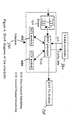
  • Fig. 4 depicts a schematic diagram of building blocks of a scheduler 330.
  • BHPs 155 arriving from switch 320 are first stored in queue 410 and are processed in a predetermined order.
  • a typical example of ordering scheme in queue 410 is a first-in-first-out (FIFO) order, although any order may be utilized with varying results.
  • Virtual queues may also be utilized and maintained for different service classes.
  • the BHP processor 420 extracts information about the DB 150 arrival time at optical switching matrix 215 and the DB 150 duration/length from the BHP.
  • BHP processor 420 then triggers data channel scheduling (DCS) module 430 and control channel scheduling (CCS) module 440.
  • DCS data channel scheduling
  • CCS control channel scheduling
  • the DCS module 430 finds a free period on one of the outbound data channels to transmit the DB 150 and determines the time required to configure the optical switching matrix 215.
  • a proper FDL buffer 235 is selected, when necessary, to avoid DB transmission conflict on an outbound data channel.
  • the CCS module 440 schedules a time to send the BHP 155 on the outbound CCG.
  • the burst offset-time is primarily employed to resolve any BHP 155 contentions on outbound CCGs.
  • the CCS module 440 is capable of and attempts to resynchronize the DB 150 and its BHP 155 by keeping the new offset time () as close as possible to its initial value ⁇ 0 .
  • the trigger of the DCS module 430 and the CCS module 440 is performed in parallel.
  • BHP processor 420 instructs switch controller 340 to configure optical switching matrix 215 accordingly, as depicted in Fig. 3 and Fig. 4.
  • the configuration information sent from the BHP processor 420 to the switch controller 340 includes: (1) incoming DCG identifier and data channel identifier; (2) outgoing DCG identifier and data channel identifier; (3) time to configure; (4) DB duration, and (5) buffer FDL identifier information (i.e. the delay time).
  • the BHP processor 420 Upon receiving an acknowledgement from the switch controller 340, the BHP processor 420 instructs the DCS and CCS modules to update their state information. It also updates the BHP (e.g., the burst offset-time and data channel identifier field among others) and passes the updated information along with time-to-send BHP information to the BHP Tx module 335. The BHP processor 420 is then ready to process the next BHP.
  • the BHP e.g., the burst offset-time and data channel identifier field among others
  • the DB 150 and its BHP 155 are simply discarded.
  • the BHP processor 420 will not process a BHP if its associated DB has already entered the optical switching matrix 215 and has gotten lost (i.e. called early burst arrival phenomenon). To prevent early burst arrivals, the input FDL 230 should be sufficiently long.
  • DB contentions on an outbound DCG are resolved by delaying the arriving DBs.
  • DBs can however only be delayed for a number of discrete time periods which are proportional to the lengths of FDLs.
  • the storage capacity of the FDL buffers depend on the number of FDLs as well as the length of each FDL.
  • the performance of optical routers in terms of burst loss ratio is determined by not only the storage capacity of FDL buffers but more importantly also by the data channel scheduling algorithm used in the data channel scheduling (DCS) module 430.
  • DCS data channel scheduling
  • Channel scheduling is critical to the design of SCU 220 and it has a critical impact on the router performance.
  • Empirical evidence suggests that using simple scheduling algorithms, like the Latest Available Unscheduled Channel (LAUC) algorithm which is also called Horizon algorithm, and increasing the FDL length leads to a decrease of burst loss ratio, but only to a certain point. A further increasing of the FDL length will adversely affect the router performance because the voids/gaps introduced by the FDL also get larger which decreases the data channel utilization. Therefore, sophisticated scheduling algorithms incorporating void filling has arisen for optical routers with FDL buffering in order to achieve desired performance.
  • LAUC Latest Available Unscheduled Channel
  • each DCS module 430 has to monitor and track busy/idle periods of its associated outbound data control group (DCG).
  • DCS module 430 searches for an eligible void/gap when scheduling an arriving DB 150. The search has to be done very quickly, e.g., in the range of 100 ⁇ 300 ns, as the DB 150 is traveling at the speed of light.
  • the complexity of the DCS module 430 increases as the number of data channels it has to schedule increases. Given the stringent real-time requirements and the state information of each data channel the DCS module 430 has to maintain, the hardware implementation of any scheduling algorithm with void filling, as noted is technically challenging.
  • the present invention relates to and focuses on the data channel scheduling module 430, also called (data) channel scheduler.
  • data channel scheduling module 430 also called (data) channel scheduler.
  • the assumptions used in the design of the channel scheduler are as follows:
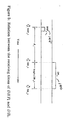
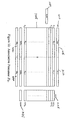
  • t s in (BHP i ) denote the time at which the first bit of BHP i is received by the switch control unit (SCU), and let t s in (DB i ) and t e in (DB i ) denote the receiving time of the first and last bit of DB i by the input FDL with respect to t s in (BHP i ), respectively, as shown in Figure 5.
  • Transmitting time interval of DB i at an optical router is denoted as[t s out (DB i ), t e out DB i )].
  • DB i Transmitting time interval of DB i at an optical router.
  • Transmitting time interval of DB i at an optical router is denoted as[t s out (DB i ), t e out DB i )].
  • DB i Transmitting time interval of DB i at an optical router.
  • a relaxed embodiment is to find a conflict-free schedule of a maximum subset of ⁇ DB i
  • the DBs that are not scheduled successfully are considered lost.
  • the set S I (i-1) is called the schedule of all DB a 's such that a ⁇ i, and its records the time intervals that have so far been used on all channels of the DCG.
  • S M (i-1) and S G (i-1) which together records all time intervals that are available for future use.
  • each E u (i-1) can be used to define a semi-unbounded time interval [E u (i-1), ⁇ ) on data channel Ch u .
  • S M (i-1) ⁇ [E u (i-1); u]
  • 1 ⁇ u ⁇ k ⁇ is used to characterize the k semi-unbounded intervals for the k data channels.
  • a gap on an outbound data channel u is a maximal time interval [l, r] such that there is no DB transmitted on channel u with transmission time that overlaps with [l, r].
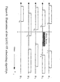
  • the heuristics of the LAUC-VF algorithm will now be described below, with reference to Fig. 6.
  • the basic idea of the LAUC-VF algorithm is to minimize voids/gaps by selecting the latest available unused/unscheduled data channel for each arriving DB.
  • the scheduler 330 Given the arrival time t of a DB with duration B to the optical switching matrix 215, the scheduler 330 first finds the outbound data channels that are available for the time period of (t, t+B). If there is at least one such channel, the scheduler selects the latest available channel, i.e., the channel having the smallest gap between t and the end of last DB just before t. In the example shown in Fig. 6, the DCG has 5 channels where D 1 , D 2 and D 5 are eligible channels at time t but D 3 and D 4 are ineligible channels at time t because the void is too small on D 3 for the DB and D 4 is busy at time t.
  • Data channel D 2 is chosen to carry the DB as t-t 2 ⁇ t-t 1 ⁇ t-t 5 . It should be noted that the transmission direction is from right to left. After choosing data channel D 2 , the state information of D 2 needs to be updated since two new voids, (t 2 ,t) and (t+B, t' 2 ), are created.
  • the algorithm is capable of inserting the DB in the first available void or gap found without regard as to whether it was the most efficient or useful gap available.
  • the processing speed may be increased since not all of the available channels need to be searched and no sorting operation as in the LAUC-VF algorithm is required.
  • the channel selection process may always revert back to the first channel in the stack and sequentially check each subsequent channel until a suitable gap is found or the DB is dropped.
  • the channel selection process could also be any predetermined or done randomly until an eligible channel is found or the DB is dropped.
  • the scheduler will then try to find the outbound data channels that are eligible at time t+L 1 (i.e. available for the time period of (t+L 1 , t+L 1 +B), and so on. If no data channels are found eligible up to time t+L q , the arriving burst is dropped. For a given time t, the data channels can be classified into unscheduled channels where no bursts are scheduled after t (e.g.D 5 ) and scheduled channels in which some DBs are already scheduled after time t (e.g.D 1 ,D 2 ,D 3 and D 4 ). The above LAUC-VF algorithm does not distinguish between scheduled and unscheduled data channels.
  • An additional embodiment provides the scheduled data channels with higher priorities. For instance, suppose there are two eligible data channels at time t, one scheduled, another unscheduled, the scheduled data channel will be selected to carry the DB. This provides additional capacity and flexibility, since it is not known when and of what length the next DB is. Therefore, by keeping available an untapped channel or an under utilized channel provides capacity that would not be there if it were arbitrarily used.
  • a scheduler does not track all of thegaps/voids in each channel, but instead remembers only one value, the unscheduled time for each channel, from which onwards the channel is free.
  • LAUC Test Available Unscheduled Channel
  • FF First Fit
  • Step (a) Find a gap [1, r; f] in S G (i-1) such that T i > 1 and T i + length(DB i ) ⁇ r. If this operation is not successful then goto Step (b); else do the following:
  • Step (e) Find L p in a subset S L ' of S L and a gap [1, r; w] in S G (i-1) such that T i + L p > 1 and T i + L p + length(DB i ) ⁇ r. If this operation is not successful then goto Step (f); else assign DB i to channel Ch w ;
  • Step (f) if Step (c) is not successful then drop DB i , else do the following operations:
  • Step (a) S G (i-1) is checked to see if DB i fits in an available gap which is larger than the threshold gap ⁇ . If such a gap [1,r;f] is found, DB i is assigned to channel Ch f , and it will be transmitted without using any delay in S L . This step tries to use the gap to transmit DB i .
  • step (b) is performed to search S M (i-1) for a channel whose semi-unbounded time interval can be used for transmission of DB i without using any output FDL delay in S L . If the answer is affirmative, DB i is assigned to such a channel Ch f that has the largest value in S M (i-1), and so that no delay in S L is used. This step implements the LAUC heuristic.
  • step (b) fails, the minimum L a in S L that allows for scheduling DB i without using gap filling (void filling) is attempted at step (c). If step (c) is successful, then the LAUC heuristic is applied at step (d) to determine a channel Ch v so that L a can be used to avoid void filling. Otherwise, Step (e) is executed.
  • step (e) executes a test of subset S L ' of S L to determine if it is possible to use a delay in S L ' and utilize an available gap in S G (i-1) to transmit DB i without causing a conflict. If this is possible, the DB i is assigned to a proper channel Ch w with a proper delay L p in the S L '.
  • step (e) If the search performed at step (e) fails but the search performed at step (c) was successful, then DB i is assigned to channel Ch v with delay L a at step (f), as provided for in step (d).
  • step (c) If L a is not found at step (c), the subset S L ' of S L is then tested to see if it is possible to use a delay L a in S L ' and a gap in S G (i-1). If steps (a), (b), (c) and (e) all fail, the DB i is dropped.
  • S M and S G are updated.
  • a newly created gap is included into S G only if its length is not smaller than a constant ⁇ . Any gap smaller than ⁇ is considered of no use for future scheduling.
  • S L ' S L at step (e), which means an exhaustive search when necessary. Exhaustive search in S L can take a lot of time. Thus, a superior approach is to search a proper subset of S L (the set S L is the set of FDLs which were defined previously).
  • the number of FDL delays to be searched is limited by a small constant c 3 , (i.e.
  • a simplified embodiment is just to use Steps (a) and (b) of the above algorithm, wherein it first searches for an eligible channel at time t, if no channel is found, it continues to search for an eligible channel at time t+L 1 , and so on. If until t+L q , no eligible channel is found, the DB will be dropped.
  • DBs and BHPs are switched in the optical switching matrix 215 and SCU 220 respectively, to maintain a precise relationship between DBs and their associated BHPs is critical for channel scheduling in optical router 200.
  • BHPs are time-stamped upon receipt by the SCU 220. Based on the time-stamp and the offset value of a BHP, the arrival time of its associated DB to the optical switching matrix 215 can be easily calculated.
  • the information used by the lookahead scheduler 330 is the timing information associated with the forthcoming DBs.
  • LAUC-VF the timing information is represented by S M and S G , wherein time is an integer variable. Assuming that the timing is accurate, a critical problem still arises as to how to represent the timing of a event (i.e. relative or absolute time values). Due to the fixed word length capacity of the system, it is desirable to use relative times rather than absolute times.
  • each node (optical router) is assumed to be equipped with a system clock that is synchronized with the input/output (I/O) bit rate.
  • operation time returns the current time of the system clock.
  • BHP' is time-stamped by the operation timestamp recv (BHP i ) ⁇ time.
  • BHPs are subject to variable delays from the times they arrive to the SCU 220 to the times they are actually processed by the schedulers.
  • BHP' is BHP i
  • DB' is DB i , the i-th DB to be scheduled by the scheduler of outbound DCG ⁇
  • t sch (BHP i ) be the time the scheduler starts to process BHP i (which is BHP').
  • BHP i is time-stamped by the operation timestamp sch (BHP i ) ⁇ time.
  • t sch (BHP 0 ) 0, and the difference t sch (BHP i ) - t sch (BHP i -1) is denoted by t interval (BHP i ).
  • the difference t sch (BHP i ) - t s in (BHP i ) is denoted by t latency (i). Since t latency (i), t interval (BHP i ), d i and length(DB i ) are relative times, we can treat t sch (BHP i ) as a new time reference point with time 0.
  • a system counter is employed to timestamp each BHP i .
  • the system counter is a c 1 -bit circular counter incremented by every pulse of the system clock, wherein c 1 is chosen such that 2 c1 > t latency (BHP i ) for any i. That is,
  • BHP i Upon receiving BHP i at the input of the SCU 220 at time t s in (BHP i ), BHP i is time-stamped by operation timestamp recv (BHP i ) ⁇ time, and at the time t sch (BHP i ), when the scheduler starts to process BHP i , it is again time-stamped by operation timestamp sch (BHP i ) ⁇ time.
  • t interval (BHP i ) timer a in the former case
  • the value of c 2 can be used to define the "window" size. It is selected to be large enough such that 2 c2 > d i + D + length(DB i ) - t latency (BHP i ) for any i, as illustrated by Eq.(7). 2 c2 > max i>0 (d i + D + L q + length(DB i )) - min i>0 t latency (BHP i )
  • DB i can be assigned to any channel without conflict when t interval (BHP i ) > 2 c2 -1.
  • relative times not only eliminates the limitation of fixed word size.
  • a number is always represented by a fixed size word (e.g., 2 bytes). If the range of the number is larger, more bits are needed to represent it. For instance, if X ranges from 0 to 7, a word of 3 bits is needed to represent it. If X ranges from 0 to 255, a word of 8 bits is needed to represent it. Therefore, it is desired to keep the range of X small, thus using fewer bits (small size word) to represent it.
  • the use of relative times also reduces the amount of information to be kept for the scheduler 325.
  • the timing information about any event occurring before the new reference point is no longer useful, and can be excluded from further consideration. More specifically, suppose that two counters timer 0 and timer 1 operate in the manner described above. At time t sch (BHP i ), instead of using S M (i-1) and S G (i-1), the present invention uses S" M (i-1) and S" G (i-1) to make decisions by treating t sch (BHP i ) as a new reference point with value 0.
  • S" M (i-1) and S" G (i-1) are updated to obtain S' M (i) and S' G (i), respectively, using t sch (BHP i ) as the reference point.
  • is a function of max i>0 (d I + D + L q ); it is no larger than a constant since max i>0 (d I + D + L q ) is upper-bounded by a constant.
  • which is a constant threshold which is selected to exclude gaps that are smaller than the constant threshold, for filtering out small gaps further reduces the size of the set of gaps to be maintained.
  • An associative memory allows parallel access of multiple memory words. It is also called a content-addressable memory (CAM). Data stored in an associative memory are addressed by their contents.
  • the advantages of an AM include its parallel accessing power and its regular structure suitable for VLSI implementation.
  • the major disadvantages of an AM are its limited scalability and high cost.
  • each word is associated in an associative memory with a simple arithmetic circuit.
  • Each AM word and its associated logic circuit form a processing element. All processing elements are capable of operating in parallel (simultaneously) under the same instruction.
  • Such a parallel processing structure is called an associative processor, and it belongs to the class of Single Instruction Stream Multiple Data Streams (SIMD) parallel architectures.
  • SIMD Single Instruction Stream Multiple Data Streams
  • the present channel scheduler repeatedly performs search operations of the form "find the smallest element a in a set S such that a ⁇ b, where b is a given comparand".
  • search operations of the form "find the smallest element a in a set S such that a ⁇ b, where b is a given comparand".
  • information stored in an associative memory needs to be maintained in sorted order, although the sorting may undertake a variety of formats.
  • the simplest sorting architecture is a linear array. Insertion, deletion and shift are basic operations of a linear array for maintaining sorted order.
  • a linear array is suggested, multidimensional or hierarchical arrays may be employed.
  • the associative processor arrays is preferred, although the present invention is not limited to this aspect, to implement the channel scheduler because (a) the state information for a data channel group (DCG) is limited so that an AM of a rather small size is adequate, and (b) the searching and updating of the state of a DCG, which is represented by the relative times of a set of events, must be carried out in parallel.
  • DCG data channel group
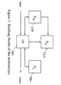
  • Fig. 7 illustrates the structure of the special purpose architecture of the present invention that implements the LAUC-VF algorithm for a DCG, for instance DCG ⁇ .
  • the input is T i ' (given by Eq. (6)) and length(BD i ) and the output is a channel number and an output FDL delay value for DB i .
  • CP control processor
  • the control processor 740 includes a simple arithmetic-logic unit (ALU)(not shown), which can be used to perform addition, subtraction and comparison operations.
  • the ALU generates all control signals for the operations of P M 710, P G 720 and P L 730.
  • the ALU takes the relative arrival time T i ' (see Eq. (6)) and burst length(BD i ) as inputs, and produces a channel number and a delay value L ri for the DB i .
  • L 810 is an associative memory of q words, L 1 , L 2 , ..., L q for q delay values in S L . It is assumed that L 1 ⁇ L 2 ⁇ ... ⁇ L q and each word is associated with a simple subtraction circuit.
  • LC 820 is a comparand register and holds the operand to be compared with the values stored in L 810.
  • LAR 830 is an address register for L 810.
  • LDR 840 is a data register for L 810, wherein LR 1 850 and LR 2 860 operate as working registers for L 810.
  • M 910 is an associative memory of k words, M 1 , M 2 , ..., M k (i.e. one for each channel of the data channel group). Each word is associated with a simple subtraction circuit for subtraction and compare operations. The words are also connected as a linear array.
  • MC 920 is a comparand register that holds the operand to be compared with.
  • MCH 930 is a memory of k words, MCH 1 , MCH 2 , ..., MCh k , with MCH j corresponding to M j . The words are connected as a linear array, and they are used to store the channel numbers.
  • MAR 1 940 and MAR 2 950 are address registers used to hold addresses for accessing M 910 and MCH 930.
  • MDR 1 960, MDR 2 970 and MCHR 980 are data registers. Together with MARs, they are used to access M 910 and MCH 930.
  • MR 990 is a working register and is employed to contain temporary data that would otherwise be lost before it is reused. Note that a pair of memory words [M i ; MCH i ], corresponds to an [E j ; u] in S M .
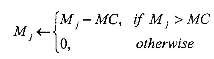
  • SEGMENT SHIFT-DOWN Given addresses a in MAR 1 940, and b in MAR 2 950, such that a ⁇ b, perform M j +1 ⁇ Mj and MCH j +1 ⁇ MCHj for all a-1 ⁇ j ⁇ b.
  • each pair (M j , MCH j ) is treated as a superword.
  • READ M and WRITE M are used to refer to RANDOM READ and WRITE operation, respectively.
  • G 1005 is an associative memory of n superwords, G 1 , G 2 , ..., G n , with each G i consisting of two words G i,1 , and G i,2 , which are called the first and second words of G i , respectively.
  • Each word is associated with a simple subtraction circuit for subtraction and compare operations.
  • the superwords are also connected as a linear array.
  • GC 1010 is a comparand register and holds a superword of two words, GC 1 1015 and GC 2 1020, which are the first and the second words of GC 1010, respectively.
  • GC 1 1015 is compared with all the first words of G 1005 and GC 2 1020 is compared with all the second words of G 1005, or only GC 1 1015 is compared with all the first words of G 1005.
  • GC 2 1020 is masked out for the operation.
  • GCH 1025 is a memory of n words, GCH 1 , GCH 2 , ..., GCH n , with GCH j corresponding to G j .
  • the words are connected as a linear array and they are used to store channel numbers.
  • GAR 1030 is an address register used to store address of a superword of G 1005 to be read or written.
  • GDR is comprised of GDR1 and GDR2 and it is a data register for G.
  • GCHR 1035 is a data register.
  • GAR 1030, GDR and GCHR together are used to access G 1005 and GCH 1025.
  • GR 1 1040 and GR 2 1050 are working registers.
  • a triple [G i,1 , G i,2 , GCH i ] corresponds to item [l, r; u] in S G .
  • each triple (G i,1 , G i,2 , GCH i ) is treated as a superword.
  • READ G and WRITE G 1005 are used to refer to RANDOM READ and WRITE on G 1005, respectively.
  • FIG. 11 A more detailed block diagram of the channel scheduler 330 architecture is illustrated in Fig. 11. In Fig. 11 only data paths are shown and the control signals are omitted. Multiplexers (MUXs) and demultiplexers (DMUXs) are used for merging and branching data paths. Dashed data paths are from/to the control processor. Logic design details of an associative processor P M* are presented in the appendix, which can be easily extended or restricted to construct P M , P G and P L
  • timer a is started at time t sch (BHP i-1 ) with initial value 0.
  • BHP i Upon receiving BHP i at time t sch (BHP i ), do the following:
  • FIG. 11 A more detailed block diagram of the channel scheduler 330 architecture is illustrated in Fig. 11. In Fig. 11 only data paths are shown and the control signals are omitted. Multiplexers (MUXs) and demultiplexers (DMUXs) are used for merging and branching data paths. Dashed data paths are from/to the control processor. Logic design details of an associative processor P M* are presented in the appendix, which can be easily extended or restricted to construct P M , P G and P L
  • the control processor in Figure 11
  • CP control processor
  • Register initializations for some operations involve parameters extracted from a BHP, system clock, and local timers. These operations are summarized in Table 1. It is assumed that the arithmetic operations in these operations are performed in the control processor (CP). All the test operations are summarized in Table 2. It is assumed that these operations are also performed by the CP. Special instructions are implemented in CP, and the control signals can be generated using microprogramming (firmware). For better speed performance, hardwired control units can be constructed.
  • T prep denote the time required for preprocessing
  • T (x) to denote the time required for Step (x).
  • Step (e2) a for-loop is utilized to check if there is a delay value among the first c 3 of S L such that by using it a gap can be found for transmitting DB;.
  • Step (e2) a for-loop is utilized to check if there is a delay value among the first c 3 of S L such that by using it a gap can be found for transmitting DB;.
  • a more sophisticated approach may be used to select delay values in S L to get a better chance for finding a feasible delay value.
  • P M 710 and P G 720 can be integrated together in real chip design by adding an additional logic circuit to distinguish channel unscheduled times and actual gaps.
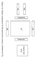
  • M* is an associate memory of n words, M* 1 , M* 2 , ..., M* n , each of length m. Each word is associated with a subtraction circuit for subtraction and compare operations. The words are also connected as a linear array.
  • CR is a comparand register. It holds the operand to be compared with.
  • AR 1 , AR 2 are address registers. They are used to hold addresses for accessing M*.
  • DR is a data register. Together with ARs, it is used to access M*.
  • a decoder is used to select the words of M* to be accessed by read, write and shift operations.
  • An encoder generates an address by a parallel search operation.
  • a control unit is used to generate control signals.
  • the decoder and encoder are separated from memory M* because of their distinctive and important functions for the proper operations of P M* .
  • PARALLEL SEARCH The value of C is compared with the values of all words M* 1 , M* 2 , ..., M * n simultaneously (in parallel). Find the smallest j such that M j * ⁇ C, and do AR 1 ⁇ j and DR 1 ⁇ M j *. If there does not exist any word M j * such that M j * ⁇ C, do AR 1 ⁇ 0.
  • the number of gate levels for a 2 p x p priority address decoder is 2p.
  • a p x 2 p decoder is a combinational circuit that has p inputs, A 0 to A p-1 , and 2 p outputs, W 0 to W 2p-1 . It is needed to generate enabling signals for accessing a memory of 2 p words. Conventionally, one and only one output W i is 1, given that A p-1 A p- 2 ... A 0 is the binary representation of i.
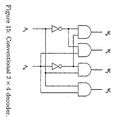
  • the 2x4 conventional decoder (“c-decoder") as shown in Fig. 15. A conventional decoder is used for random access of a memory.
  • a new address decoder is designed which contains a conventional decoder as a subcircuit.
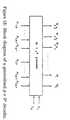
  • a special p x 2 p decoder is presented, called a bipartition decoder ("b-decoder"). It has p inputs, A 0 to A p-1 , and 2 p outputs, W 0 to W 2p-1 .
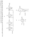
  • the circuit for the 1x2 b-decoder is shown in Fig. 16(A).
  • a p x 2 p b-decoder can be constructed using two copies of a (p-1) x 2 p-1 b-decoder, as shown in Fig.
  • a 2p x 2 p g-decoder has 2p inputs A 1,0, A 1,1 ..., A 1,p-1 , A 2,0 , A 2,1 ..., A 2,p-1 , 2 p outputs W 0 , W 1 , ..., W 2p-1 , and two control signals S 0 and S 1 .
  • W 1,i , 0 ⁇ i ⁇ 2 p be the outputs of the c-decoder
  • W 2,i, , 0 ⁇ i ⁇ 2 p be the outputs of the first b-decoder
  • W 3,i , 0 ⁇ i ⁇ 2 p be the outputs of the second b-decoder
  • W i , 0 ⁇ i ⁇ 2 p be the outputs of the g-decoder.
  • W i ( S 1 ⁇ S 0 ⁇ W 1, i ) ⁇ ( S 1 ⁇ S 0 ⁇ W 2, i ) ⁇ ( S 1 ⁇ S 1 ⁇ W 2, i ⁇ W 3, i )
  • ⁇ and ⁇ are logical AND and OR operations, respectively.
  • the block diagram of a g-decoder is shown in Figure 18.
  • the internal structure of a memory of n words with m bits per word consists of n x m storage cells and the associated logic needed for selecting words for reading and writing.
  • a flip-flop is used to store one bit.
  • a design of a storage cell of the present invention, called basic cell (BC) is shown in Fig. 19. It uses an RS flip-flop to store a bit, and it has four control signals, X, Y, Clr and R/W.
  • the relevant control functions of the BC are summarized in Table 5. In this table, x indicates a "don't care" condition (either 0 or 1).
  • the parallel subtraction and search operations require to perform subtraction and compare operation on each word and the operand in CR. Since the compare operation can be implemented by subtraction, there is a need to associate an m-bit parallel subtractor with each memory word.
  • the basic circuit unit of the parallel subtractor is called a subtractor cell (SC), and its logic diagram and block diagram are shown in (a) and (b) of Figure 20, respectively.
  • FA stands for full adder.
  • the control of the SC is summarized in Table 6.
  • an m-bit parallel subtractor can be constructed as shown in Figure 20(c).
  • F F m-1 F m-2 ...F 0 be the output of this circuit.
  • Sub/Trans 1
  • this circuit performs a subtraction operation by an addition
  • F B + C + 1
  • Carry m 1 if B ⁇ C.
  • the SCs associated with a memory word are connected in such a way to implement parallel subtraction, search (compare) and shift operations.
  • FIG. 21 The design of a memory cell (MC) of the associative memory M* is shown in Figure 21.
  • Each MC is constructed using a pair of BC and SC.
  • MUX multiplexer
  • the roles of all inputs, output, and control lines can be understood when MCs are connected as a two-dimensional array.
  • P M* The configuration of P M* that consists of 4 words with 3 bits per word is shown in Figure 22.
  • the 4x2 encoder is the priority encoder (see Figure 14 (b))
  • the 4x4 decoder is the g-decoder (see Figure 17).
  • Each MC has a structure as shown in Figure 21.
  • Control signals S 0 , S 1 , S 2 , S 3 , R/W, I 0 , I 1 , and I 2 are generated by the CU (control unit).
  • the control signal values (except S 0 , S 1 , S 2 and S 3 ) for the operations of P M* are listed in Table 7, wherein the clock signals are omitted.
  • the inputs SB i of the encoder is the leftmost carry bit of the subtractor associated with word M i *.
  • the control signals required for each of the operations of P M* are listed in Table 7, where an x symbol indicates a "don't care condition"' (i.e. either a 0 or a 1).
  • n the number of words in M*, be 2 p - 1. Then a 2p x 2 p g-decoder and a 2 p x p p-encoder is used. It is important to note that word M* 0 is a dummy word, which is not be used to store information. This is because address 0 is used to signify that a parallel search operation does not produce a valid address. By treating word M* 0 as a dummy word, the circuit is simplified considerably.
  • Associative processor P M is an extension of P M* by associating an MCH word with each word in M.
  • Associative processor P G further extends P by allowing parallel searching with a single comparand and double comparands.

Landscapes

  • Engineering & Computer Science (AREA)
  • Computer Networks & Wireless Communication (AREA)
  • Data Exchanges In Wide-Area Networks (AREA)
  • Optical Communication System (AREA)

Abstract

A system and method for implementing channel scheduling algorithms in an optical router wherein a scheduler operates pursuant to an algorithm and is capable of determining the availability of outbound data channels capable of carrying a data packet of duration B. The scheduler is further capable of selecting one channel from available data channels and assigning the data packet to the selected channel. The scheduler then updates state information of the selected data channel, but if no data channel is available to carry the data packet the data packet is dropped.

Description

TECHNICAL FIELD OF THE INVENTION
The present invention relates generally to optical routing and scheduling of data packets, and more specifically to an optical routing and scheduling of data packets employing a void filling algorithm and fiber delay lines (FDLs) as an optical buffer.
DISCUSSION OF THE RELATED ART
One of the major trends in networking in late 1990's has been a relentless growth in demand for bandwidth in both enterprise and service provider networks. Driving the need for more bandwidth is a combination of factors. More users are connecting as the commercial Internet offers a new online experience for consumers. Internet computing applications, including multi-tier distributed databases, interactive multimedia communication, and electronic commerce rely on the network and demand network resources. A new generation of high-speed Internet access is emerging to meet bandwidth demands and further amplify core bandwidth requirements.
At the same time, competitive pressures make it imperative that networking costs be reduced even as the demand for capacity and new services increases. Successful companies are constantly on the lookout for new technologies which can provide a competitive edge and increase their cost effectiveness.
Optical networking has emerged as a solution to the bandwidth crunch. In particular, one new optical technology-Dense Wavelength Division Multiplexing (DWDM)―promises to increase the capacity and performance of existing fiber optic backbones. DWDM offers a capacity upgrade solution with greater scalability and lower cost than available alternatives.
Wavelength Division Multiplexing (WDM) is a technique for increasing the information-carrying capacity of optical fiber by transmitting multiple signals simultaneously at different wavelengths (or "colors") on the same fiber. In effect, WDM converts a single fiber into multiple "virtual fibers," each driven independently at a different wavelength. Systems with more than a small number of channels (two or three) are considered Dense WDM (DWDM) systems. Nearly all DWDM systems operate across a range of wavelengths in the 1550nm low-attenuation window.
A DWDM system generally includes optical transmitters (lasers), an optical multiplexer and an demultiplexer, optical amplifiers and optical receivers. DWDM systems use high resolution, or narrowband, lasers transmitting in the 1550nm wavelength band.
The optical multiplexer combines the transmit signals at different wavelengths onto a single optical fiber, and the demultiplexer separates the combined signal into its component wavelengths at the receiver. Several technologies are currently used for optical multiplexing and demultiplexing, including thin-film dielectric filters and various types of optical gratings. Some (de)multiplexers are constructed as completely passive devices, meaning they require no electrical input. Passive optical (de)multiplexers behave essentially like very high precision prisms to combine and separate individual colors of the WDM signal.
The optical receiver is responsible for detecting an incoming lightwave signal and converting it to an appropriate electronic signal for processing by the receiving device. Optical receivers are very often wideband devices able to detect light over a relatively wide range of wavelengths from about 1280-1580nm. This is the reason why some seemingly incompatible devices can actually inter-operate. For instance, directly connecting two otherwise compatible network interfaces with different transmitter wavelengths is usually not a problem, even though one end may be transmitting at 1310nm and the other at 1550nm.
An additional benefit of the optical amplifier is that as a strictly optical device, it is a protocol- and bit rate-independent device. In other words, an optical amplifier operates the same way regardless of the framing or bit rate of optical signals. This allows a great deal of flexibility in that an optically amplified link can support any combination of protocols (e.g. ATM, SONET, Gigabit Ethernet, PPP) at any bit rate up to a maximum design limit.
With the deployment of DWDM optical fiber transmission systems to accommodate the ever increasing demand for bandwidth, driven by Internet applications, routers/switches are still likely to be the bottleneck of the next generation of Internet backbones. Using the DWDM technology, one can already achieve the transmission capacity of 320 Gbps per fiber commercially. The need for extremely high capacity routers, in the range of one terabits per second (Tbps) and beyond, is expected in the near future.
Optical burst switching (OBS) is an attractive technology in building tera-bit optical routers and realizing the Internet Protocol (IP) over dense wavelength division multiplexing (DWDM). An intrinsic feature of OBS is the separate transmission and switching of data bursts 150 (payload) and their headers 155 (called burst header packets (BHP)) on data and control channels/wavelengths, respectively. Due to the lack of an optical RAM (random access memory), fiber delay lines (FDLs) are used in optical routers to resolve burst conflicts on outbound data channels. In a simplified optical router architecture with N input fibers and N output fibers each fiber has one data channel group (DCG) of (K-1) channels and one control channel group (CCG) of one channel.
For optical routers using FDL buffering, there is a scheduler for each outbound DCG which schedules the arriving data bursts 150 that are to be routed to the same outbound DCG. The scheduler is a key component in the switch control unit. Any channel scheduling algorithm used in the scheduler will directly affect the router performance in terms of throughput and burst loss ratio. The prior art has not produced channel scheduling algorithms capable of providing acceptable throughput and burst loss ratio.
What is needed are sophisticated channel scheduling algorithms incorporating void filling in order to achieve the desired router performance. For any scheduling algorithm with void filling, each scheduler needs to keep track of the busy/idle periods of every data channel of its associated outbound DCG. The scheduler searches for an eligible void/gap when scheduling an arriving data burst. The search has to be done very quickly, e.g., in the range of a few hundred nanoseconds (say 100-300ns), as the data burst is transmitted at the speed of light. As the number of channels handled by the scheduler increases, so does the complexity of the scheduler.
A scheduler that has to maintain the hardware implementation of a scheduling algorithm with void filling is a technically challenging endeavor, given the stringent real-time requirements and the state information of each data channel.
Various channel scheduling algorithms with and without void filling have been proposed such as the Latest Available Unused Channel (LAUC) algorithm, (also called the Horizon algorithm) and the Latest Available Unused Channel with Void Filling (LAUC-VF) algorithm (and variations on that theme), and other void filling scheduling algorithms. In terms of router performance (burst loss ratio) simulation studies have shown that the LAUC-VF is probably one of the best among all the scheduling algorithms. Despite the studies and the need for such algorithms, no hardware implementation design is available to implement these algorithms.
SUMMARY OF THE INVENTION
Accordingly the present invention provides a scheduling algorithm incorporating void filling and a hardware implementation design capable of implementing the algorithm wherein the desired performance is capable of scheduling a data packet in no more than a few hundred nanoseconds.
The present invention has been made in view of the above circumstances and has as an object to employ a special-purpose parallel processing architecture in the design of the scheduler to meet the stringent real-time requirements. Specifically, the present invention contemplates the use of an associative memory to store the state information of channels and to use associative processor arrays to implement void/gap searches and channel state information updates. The use of the associative processor arrays to implement the channel scheduler provides several advantages. One advantage of the present invention is the state information for a DCG is limited so that an associative memory of a rather small size is adequate. Another advantage is the search and update of the state information of a DCG, which is represented by the relative times of a set of events, is carried out in parallel.
The implementation of the LAUC-VF algorithm or any of the other viable algorithms, requires that the channel state information be frequently updated to reflect the change in time. To solve this problem, the present invention employs the use of relative timing verses absolute timing for representing channel state information. This is achieved by taking a reference point of the relative time, such as at the time the scheduler starts to process a BHP. At each new reference point the state information of all the channels of a DCG are updated simultaneously. Associative processors PG, PM and PL are used to store all the voids, channel unscheduled times and delay times of FDLs, respectively. Search and update functions are also provided and substantially enhance the utility of the algorithm of the present invention. A control processor (CP) coordinates the operations of the processors PG, PM and PL.
In processor PG, voids are stored in a given order according to their starting times. Similarly, in processors PM and PL, the channel unscheduled times and delay times of FDLs are also stored in a given order. Searching for a void can easily be performed by one operation called "Parallel Double-Comparand Search". Inserting new voids into the PG processor is performed by the "Bipartition Shift-Up" and "Bipartition Shift-Down" operations. Processors PG and PM are first used together to find the latest available unused channel without using any FDL buffer. In case FDL are used processor PL will be involved to determine which FDL buffer will be used.
The present invention contemplates the use of a special-purpose parallel processing architecture in the design of schedulers in optical routers, by providing design methodologies for implementing a class of scheduling algorithms with and without void filling.
A further aspect of the present invention is to provide a system for scheduling of data packets in an optical router operating pursuant to an algorithm capable of selecting a suitable outbound channel in real time.
Additional aspects and advantages of the invention will be set forth in part in the description which follows, and in part that will be obvious from the description, or may be learned by practice of the invention. These aspects and advantages of the invention will be realized and attained by means of the elements and combinations particularly pointed out in the appended claims.
To achieve the aspects of the present invention and in accordance with the purpose of the invention, as embodied and broadly described herein, an aspect of the invention can be characterized as a method for implementing channel scheduling algorithms in an optical router, the method including the steps of determining availability of outbound data channels capable of carrying a data packet of duration B and selecting one channel from available data channels. The algorithm further assigns the data packet to the selected channel and updates state information of the selected data channel, wherein if no data channel is available to carry the data packet the data packet is dropped. The algorithm also is capable of determining whether a time delay L can be introduced to shift the arrival time of the data packet via a fiber delay line (FDL), from t to (t+L) to avoid the dropping of the data packet. If such a delay L is available, the algorithm assigns the data packet a delay time equal to L and assign s the appropriate outbound data channel
The assigning of a channel further includes selecting a fiber and a wavelength from the outbound data channel group to transmit the data packet wherein the data packet may be of a fixed or variable length.
A further aspect of the present invention can be characterized as a system for implementing channel scheduling algorithms in an optical router. The system includes a scheduler, operating pursuant to an algorithm. The scheduler is capable of determining availability of outbound data channels capable of carrying a data packet of duration B and selecting one channel from available data channels. The system then assigns the data packet to the selected channel and updates state information of the selected data channel, but if no data channel is available to carry the data packet the data packet is dropped.
A still further aspect of the invention can be characterized as an apparatus for implementing channel scheduling algorithms in an optical router, the apparatus including means for determining the availability of outbound data channel capable of carrying a data packet of duration B and selecting one channel from the available data channels. The apparatus also includes means for assigning the data packet to the selected channel and means for updating state information of the selected data channel, but if no data channel is available to carry the data packet, the packet is dropped. The means for determining the availability of an outbound channel includes the use of associative processors PG and PM to store and search voids/gaps and channel unscheduled time for which a channel is free, respectively. PG is capable of storing the set of voids/gaps and the corresponding channels and to conduct of parallel search of the set of voids gaps for an available void/gap which is capable of accommodating a data packet. PM is capable of storing a set of channel unscheduled times from which a channel is free and the corresponding channels and to conduct a parallel search for an available unscheduled time for which a channel is free.
It is to be understood that both the foregoing general description and the following detailed description are exemplary and explanatory only and are not restrictive of the invention, as claimed.
BRIEF DESCRIPTION OF THE DRAWINGS
The accompanying drawings, which are incorporated in and constitute a part of this specification, illustrate several embodiments of the invention and together with the description, serve to explain the principles of the invention.
  • Fig. 1 is a diagram of an optical burst-switched network;
  • Fig. 2 illustrates a general architecture of an optical router of the present invention;
  • Fig. 3 is a block diagram of the switch control unit of the present invention;
  • Fig. 4 is a block diagram of the scheduler of the present invention;
  • Fig. 5 illustrates relationships between receiving times of a burst header packet (BHP) and a data burst (DB) of the present invention;
  • Fig. 6 illustrates a Latest Available Unused Channel with Void Filing (LAUC-VF) scheduling algorithm of the present invention;
  • Fig. 7 illustrates a channel scheduler architecture of the present invention;
  • Fig. 8 depicts an internal structure of an associate processor PL of the present invention;
  • Fig. 9 depicts an internal structure of an associate processor PM of the present invention;
  • Fig. 10 depicts an internal structure of an associate processor PG of the present invention;
  • Fig. 11 is a block diagram of the channel scheduler of the present invention;
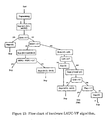
  • Fig. 12 depicts a flow chart of an implementation of an LAUC-VF algorithm of the present invention;
  • Fig. 13 shows a block diagram of the associate memory architecture for the PM* processor of the present invention;
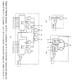
  • Fig. 14(a) is a logic diagram of a 2 X 1 p-encoder;
  • Fig. 14(b) is a logic diagram of a 4 X 2 p-encoder constructed using two 2 X 1 p-encoders of Fig. 14(a);
  • Fig. 14(c) is a logic diagram of a 16 X 4 p-encoder constructed using two 8 X 3 p-encoders;
  • Fig. 15 is a logic diagram of a conventional 2 X 4 decoder;
  • Figs. 16(A), 16(B) and 16(C) are logic diagrams of a Bipartition decoder of the present invention;
  • Fig. 17 is a logic diagram of a general 4 X 4 decoder;
  • Fig. 18 is a block diagram of a generalized px2P decoder;
  • Fig. 19(A) depicts a logic diagram of a basic cell of the present invention;
  • Fig. 19(B) is a block diagram of a basic cell of the present invention;
  • Fig. 20(A) depicts an arithmetic subtractor stage of the present invention;
  • Fig. 20(B) is a block diagram of a subtractor cell
  • Fig. 20(C) depicts an arithmetic circuit associated with every word of the present invention;
  • Fig. 21 depicts a schematic diagram of a memory cell of the present invention; and
  • Fig. 22 depicts a schematic diagram of the associative processor PM* of the present invention.
  • DESCRIPTION OF THE PREFERRED EMBODIMENT
    Reference will now be made in detail to the present embodiments along with exemplary embodiments and alternate embodiments of the invention, examples of which are illustrated in the accompanying drawings. Wherever possible, the same reference numbers will be used throughout the drawings to refer to the same or like parts.
    In accordance with the invention, the present invention includes a method for implementing channel scheduling algorithms in an optical router, the method includes the steps of determining availability of outbound data channels capable of carrying a data packet of duration B and selecting one channel from available data channels. The algorithm further assigns the data packet to the selected channel and updates state information of the selected data channel, wherein if no data channel is available to carry the data packet the data packet is dropped. The algorithm also is capable of determining whether a time delay L ca introduced to shift the arrival time of the data packet via a fiber delay line (FDL), from t to (t+L) to avoid the dropping of the data packet. If such a delay L is available, the algorithm assigns the data packet a delay time equal to L and assigns the appropriate outbound data channel.Assigning of a channel further includes selecting a fiber and a wavelength from the outbound data channel group to transmit the data packet wherein the data packet may be of a fixed or variable length.
    The present invention further includes a system for implementing channel scheduling algorithms in an optical router. The system includes a scheduler, operating pursuant to an algorithm. The scheduler is capable of determining availability of outbound data channels capable of carrying a data packet of duration B and selecting one channel from available data channels. The system then assigns the data packet to the selected channel and updates state information of the selected data channel, but if no data channel is available to carry the data packet the data packet is dropped.
    The invention will be further clarified by the following examples, which are intended to be purely exemplary of the invention.
    Fig. 1 depicts an optical burst-switched network 100 which includes core routers 105, 106, 107, 108, and 109, electronic edge routers 130, 135 and 140 connected by Dense Wavelength Division Multiplexing (DWDM) links 145. Data bursts (DBs) 150 are transferred by the OBS network 100. A DB 150 is routed to its destination by a header burst packet (BHP) 155, which carries routing information in the form of a data packet.
    A general architecture of an optical core router 200, as illustrated in Figure 2, has N input fibers and M output fibers. The router primarily consists of an optical switching matrix 215 and a switch control unit (SCU) 220.
    The optical router 200 also includes routing and signaling processors 225, an input FDL 230 and a FDL buffer 235 deployed by optical switching matrix 215. The FDL buffer 235 can be contained or incorporate within switching matrix 215. The optical router 200 further includes data channel group 240 and control channel group 245 functionality. Channel mapping is used to logically decouple the channels from physical fibers. For example, in Figure 2, the optical router has L incoming data/control channel groups and L' outgoing data/control channel groups. Note that for each data channel group (DCG), there is an associated control channel group (CCG). A DCG and CCG pair connects two adjacent optical routers, although channels of the DCG/CCG may not be physically carried on the same fiber.
    Typically, the router is symmetric with N input and N output fibers, where each fiber has one DCG of (K-1) channels and one CCG of one channel. The data channels are connected to the optical switching matrix 215 and control channels are terminated at the SCU 200.
    The routing processor 225 runs routing (and other control) protocols and computes forwarding tables for the SCU 220. Thus, forwarding of BHPs and their associated DBs can be connectionless or connection-oriented (prior path establishment through signaling). The input fiber delay line (FDL) 230 delays the arriving DBs, thus allowing SCU 220 to have sufficient time to process the associated BHPs and configure optical switching matrix 215 to let DBs fly-through. There is no optical-to-electronic (O/E) and electronic-to-optical (E/O) conversions for DBs 150 in the optical router 220.
    A non-blocking optical switching matrix 215 is considered, in which an arriving DB 150 on an inbound data channel can be switched to any idle outbound data channel. FDLs 235 are used as optical buffers to resolve burst contentions on outbound DCGs.
    The SCU 220 functions similarly to an electronic router. A block diagram of SCU 220 is shown in Figure 3, where the packet processor 305 performs layer 1 and layer 2 decapsulation functions and attaches a time-stamp to each arriving BHP 155, which records the arrival time of the associated DB 150 at the optical switching matrix 215. The time-stamp is the sum of the BHP 155 arrival time, the burst offset-time carried by the BHP 155 and the delay introduced by the input FDL 230. Forwarder 315 performs the forwarding table lookup to decide on which outbound CCG to forward the BHP. The associated DB is forwarded to the corresponding DCG. The switch 320 in SCU 220 switches the BHP 155 to the scheduler 330 of the destined outbound CCG. There is a scheduler for each outbound DCG and CCG pair. Its function is to schedule the incoming DBs (and BHPs) to be switched to the same outbound DCG (and CCG). For the non-blocking optical switching matrix 215, each scheduler needs only to keep track of the usage of its associated outbound DCG and CCG. The switch controller 340 configures the optical switching matrix 215 according to the information given by the schedulers. The BHP transmission (Tx) 335 module is responsible for the transmission of BHPs on the outbound CCG 255.
    The scheduler 330 is a critical component of SCU 220. Fig. 4 depicts a schematic diagram of building blocks of a scheduler 330. BHPs 155 arriving from switch 320 are first stored in queue 410 and are processed in a predetermined order. A typical example of ordering scheme in queue 410 is a first-in-first-out (FIFO) order, although any order may be utilized with varying results. Virtual queues may also be utilized and maintained for different service classes. Once receiving a BHP 155 from queue 410, the BHP processor 420 extracts information about the DB 150 arrival time at optical switching matrix 215 and the DB 150 duration/length from the BHP. BHP processor 420 then triggers data channel scheduling (DCS) module 430 and control channel scheduling (CCS) module 440. In one embodiment the trigger of the DCS module 430 and the CCS module 440 is performed in a sequential order. The DCS module 430 then finds a free period on one of the outbound data channels to transmit the DB 150 and determines the time required to configure the optical switching matrix 215. A proper FDL buffer 235 is selected, when necessary, to avoid DB transmission conflict on an outbound data channel. Once the DB 150 departure time from the optical switching matrix 215 is determined, the CCS module 440 schedules a time to send the BHP 155 on the outbound CCG. The burst offset-time is primarily employed to resolve any BHP 155 contentions on outbound CCGs. The CCS module 440 is capable of and attempts to resynchronize the DB 150 and its BHP 155 by keeping the new offset time () as close as possible to its initial value τ0.
    To speedup the scheduling process, in another embodiment of the scheduler 330, the trigger of the DCS module 430 and the CCS module 440 is performed in parallel.
    Once scheduling DB 150 and its BHP 155, BHP processor 420 instructs switch controller 340 to configure optical switching matrix 215 accordingly, as depicted in Fig. 3 and Fig. 4. The configuration information sent from the BHP processor 420 to the switch controller 340 includes: (1) incoming DCG identifier and data channel identifier; (2) outgoing DCG identifier and data channel identifier; (3) time to configure; (4) DB duration, and (5) buffer FDL identifier information (i.e. the delay time).
    Upon receiving an acknowledgement from the switch controller 340, the BHP processor 420 instructs the DCS and CCS modules to update their state information. It also updates the BHP (e.g., the burst offset-time and data channel identifier field among others) and passes the updated information along with time-to-send BHP information to the BHP Tx module 335. The BHP processor 420 is then ready to process the next BHP.
    In the event that either the required delay time for the DB is too long (e.g. larger than the delay that could be provided by the FDL buffer) or the BHP cannot be sent on the outbound CCG with a nonnegative offset time or there is not enough time to process the BHP before the DB enters the optical switching matrix 215, the DB 150 and its BHP 155 are simply discarded. The BHP processor 420 will not process a BHP if its associated DB has already entered the optical switching matrix 215 and has gotten lost (i.e. called early burst arrival phenomenon). To prevent early burst arrivals, the input FDL 230 should be sufficiently long.
    For optical routers using fiber delay line (FDL) buffers, DB contentions on an outbound DCG are resolved by delaying the arriving DBs. DBs can however only be delayed for a number of discrete time periods which are proportional to the lengths of FDLs. The storage capacity of the FDL buffers depend on the number of FDLs as well as the length of each FDL. The performance of optical routers in terms of burst loss ratio is determined by not only the storage capacity of FDL buffers but more importantly also by the data channel scheduling algorithm used in the data channel scheduling (DCS) module 430.
    Channel scheduling is critical to the design of SCU 220 and it has a critical impact on the router performance. Empirical evidence suggests that using simple scheduling algorithms, like the Latest Available Unscheduled Channel (LAUC) algorithm which is also called Horizon algorithm, and increasing the FDL length leads to a decrease of burst loss ratio, but only to a certain point. A further increasing of the FDL length will adversely affect the router performance because the voids/gaps introduced by the FDL also get larger which decreases the data channel utilization. Therefore, sophisticated scheduling algorithms incorporating void filling has arisen for optical routers with FDL buffering in order to achieve desired performance.
    To properly employ void filling, each DCS module 430 has to monitor and track busy/idle periods of its associated outbound data control group (DCG). DCS module 430 searches for an eligible void/gap when scheduling an arriving DB 150. The search has to be done very quickly, e.g., in the range of 100 ∼ 300 ns, as the DB 150 is traveling at the speed of light. Obviously, the complexity of the DCS module 430 increases as the number of data channels it has to schedule increases. Given the stringent real-time requirements and the state information of each data channel the DCS module 430 has to maintain, the hardware implementation of any scheduling algorithm with void filling, as noted is technically challenging.
    The present invention relates to and focuses on the data channel scheduling module 430, also called (data) channel scheduler. The assumptions used in the design of the channel scheduler are as follows:
  • (1) Each DCG has k data channels that are denoted by Ch1, Ch2, ...,Chk. This assumption simplifies the presentation. In reality, different DCGs may have different number of channels;
  • (2) Each outbound DCG is equipped with a scheduler, which is responsible for scheduling DBs that are switched to the DCG;
  • (3) The BHPs associated with the DBs to be transmitted on the same outbound DCG are scheduled in the order they are received at the scheduler for that DCG. For simplicity, it is assumed that this is a linear order;
  • (4) BHPi includes an offset field di that specifies the time between the transmission of the first bit of BHPi and the first bit of DBi;
  • (5) BHPi includes a length field length(DBi) that specifies the length of DBi. Without loss of generality, assume that length(DBi) is quantified in terms of time (if this is not the case, its corresponding time can be determined by the data channel transmission bit rate);
  • (6) Each DBi is delayed by the input FDL for a fixed D time before it enters the optical switching matrix 215; and
  • (7) There is a set SL of q available FDL delay times, S L = {L1, L2, ..., Lq}, that can be selected by the scheduler for DBs to go through the optical switching matrix 215.
  • Let ts in (BHPi) denote the time at which the first bit of BHPi is received by the switch control unit (SCU), and let ts in (DBi) and te in (DBi) denote the receiving time of the first and last bit of DBi by the input FDL with respect to ts in (BHPi), respectively, as shown in Figure 5. Thus, ts in (DBi) = ts in (BHPi) + di and te in (DBi) = ts in (DBi) + length(DBi).
    Let ts out (DBi) and te out(DBi) denote the transmitting of DBi over an outbound data channel. Then, ts out (DBi) = ts in(BHPi) + d i + D + Lri and te out(DBi) = ts out(DBi) + length(DBi).    where Lri is an output delay time selected from SL" = SL {L0}, with L0 = 0.
    Transmitting time interval of DBi at an optical router is denoted as[ts out(DBi), te outDBi)]. There is a conflict between DBi and DBj if they are transmitted using the same outbound data channel and [ts out(DBi),te out(DBi)][ts out(DBj), te out(DBj)] Ø.
    Transmitting time interval of DBi at an optical router is denoted as[ts out(DBi), te outDBi)]. There is a conflict between DBi and DBj if they are transmitted using the same outbound data channel and [ts out(DBi),te out(DBi)]∩[ts out(DBj), te out(DBj)] ≠ Ø.
    Based on ts in(BHPi), d; and length(DBi), i = 1, 2, 3, ..., for the same outbound DCG, assign each DBi to an outbound data channel Chu, 1 ≤u ≤ k, and select a delay time Lri from SL" for DBi such that there is no conflict between DBi and DBj, j ≠ i. Such a channel assignment is called a conflict-free schedule. The scheduling time (decision-making time) for each (BHPi, DBi) pair should be no more than a bounded time.
    Due to the real-time constraints, limited lookahead knowledge about future bursts, and the adopted cost/performance trade-off, it may not be always possible to find a conflict-free schedule for all DBs. Thus, the present invention has many alternate embodiments. A relaxed embodiment is to find a conflict-free schedule of a maximum subset of {DBi | i = 1, 2, 3, ...} in the least possible time, based on ts in(BHPi), d; and length(DBi), i = 1, 2, 3, ..., for the same outbound DCG. The DBs that are not scheduled successfully are considered lost.
    An analysis of the transmission delay is begun by comparing Eq. (3) with Eq. (1) (respectively, Eq. (4) with Eq. (2)). This comparison reveals that an additional transmission delay D+Lri is introduced at each node. While D is fixed, it is desirable to minimize delay Lri whenever possible.
    If it is assumed that the BHPs arrive at the channel scheduler 330 of a tagged outbound DCG, say DCG γ, are BHPi, (i = 1, 2, ...,n). Set SI(i-1) = {[ts out(DBa), te out(DBa); ca] |1 ≤ a ≤ i-1, 1 ≤ ca ≤ k} is used to represent the state of the k channels of the DCG at the time DBi is being scheduled, where [ts out(DBa), te out(DBa); ca] represents the fact that DBa is scheduled to be transmitted using data channel Chca of the tagged outbound DCG with starting time ts out(DBa) and ending time te out(DBa). Since the scheduling of DBa, 1 ≤ a ≤ i-1, is conflict-free, [ts out(DBx), te out(DBx)] ∩ [ts out(DBy),te out(DBy)] = Ø, for 1 ≤ x, y ≤ i-1, x ≠ y and cx = cy. By Eq. (3) and Eq. (4), ts out(DBa) = ts in(BHPa) + da + D + Lra and te out(DBa) = ts in(BHPa) + da + D + Lra + length(DBa), where Lra is an output FDL delay time selected from SL U {L0}, with L0 = 0. The set SI(i-1) is called the schedule of all DBa's such that a < i, and its records the time intervals that have so far been used on all channels of the DCG. Using SI(i-1) two sets are defined, SM(i-1) and SG(i-1), which together records all time intervals that are available for future use.
    For 1 ≤ u ≤ k, [SuI(i-1) = {[ts out(DBa),te out(DBa);ca] | [ts out(DBa),te out(DBa); ca] □ SI(i-1) and ca = u}
    Figure 00120001
    Clearly, each Eu(i-1) can be used to define a semi-unbounded time interval [Eu(i-1), ∞) on data channel Chu.
    SM(i-1) = {[Eu(i-1); u] | 1≤ u ≤ k} is used to characterize the k semi-unbounded intervals for the k data channels.
    A gap on an outbound data channel u, represented by g = [l, r; u], is a maximal time interval [l, r] such that there is no DB transmitted on channel u with transmission time that overlaps with [l, r]. Clearly, a gap can be of two forms: (i) g = [0, ts out(DBx); u], and there does not exist any [ts out(DBy), te out(DBy); u] such that ts out(DBy) ≤ ts out(DBx), and (ii) g = [te out(DBx), ts out(DBy); u], and there does not exists [ts out(DBz), te out(DBz); u]□ Si u(i-1) such that either [ts out(DBx),te out(DBx)] ∩ [ts out(DBz),te out(DBz)] ≠ Ø or [ts out(DBy),te out(DBy)] ∩ [ts out(DBz), te out(DBz)] ≠ Ø. SG(i-1) is used to denote the set of all gaps defined by schedule SI(i-1).
    The heuristics of the LAUC-VF algorithm will now be described below, with reference to Fig. 6. The basic idea of the LAUC-VF algorithm is to minimize voids/gaps by selecting the latest available unused/unscheduled data channel for each arriving DB.
    Given the arrival time t of a DB with duration B to the optical switching matrix 215, the scheduler 330 first finds the outbound data channels that are available for the time period of (t, t+B). If there is at least one such channel, the scheduler selects the latest available channel, i.e., the channel having the smallest gap between t and the end of last DB just before t. In the example shown in Fig. 6, the DCG has 5 channels where D1, D2 and D5 are eligible channels at time t but D3 and D4 are ineligible channels at time t because the void is too small on D3 for the DB and D4 is busy at time t. Data channel D2 is chosen to carry the DB as t-t2 < t-t1 < t-t5. It should be noted that the transmission direction is from right to left. After choosing data channel D2, the state information of D2 needs to be updated since two new voids, (t2,t) and (t+B, t'2), are created.
    In an alternative embodiment, called First Fit with Void Filling (FF-VF), the algorithm is capable of inserting the DB in the first available void or gap found without regard as to whether it was the most efficient or useful gap available. In this embodiment the processing speed may be increased since not all of the available channels need to be searched and no sorting operation as in the LAUC-VF algorithm is required. In this embodiment the channel selection process may always revert back to the first channel in the stack and sequentially check each subsequent channel until a suitable gap is found or the DB is dropped.
    In a still further embodiment the scheduling of the search process for locating an available gap in the available channels may follow a round robin process beginning the next search from the point where the previous successful insertion of the DB was preformed. For instance if there are n =5 available channels to select from and the previous available gap was found on n = 2 then the next attempt will be at channel n = 3 and so on. The channel selection process could also be any predetermined or done randomly until an eligible channel is found or the DB is dropped.
    In the case where all the data channels are ineligible at time t, the scheduler will then try to find the outbound data channels that are eligible at time t+L1 (i.e. available for the time period of (t+L1, t+L1+B), and so on. If no data channels are found eligible up to time t+Lq, the arriving burst is dropped. For a given time t, the data channels can be classified into unscheduled channels where no bursts are scheduled after t (e.g.D5) and scheduled channels in which some DBs are already scheduled after time t (e.g.D1,D2,D3 and D4). The above LAUC-VF algorithm does not distinguish between scheduled and unscheduled data channels.
    An additional embodiment provides the scheduled data channels with higher priorities. For instance, suppose there are two eligible data channels at time t, one scheduled, another unscheduled, the scheduled data channel will be selected to carry the DB. This provides additional capacity and flexibility, since it is not known when and of what length the next DB is. Therefore, by keeping available an untapped channel or an under utilized channel provides capacity that would not be there if it were arbitrarily used.
    In a still additional embodiment of the present invention a scheduler does not track all of thegaps/voids in each channel, but instead remembers only one value, the unscheduled time for each channel, from which onwards the channel is free. In this embodiment, one example is the LAUC (Latest Available Unscheduled Channel) algorithm, a degeneration of LAUC-VF algorithm. Another example is the FF (First Fit) algorithm, a degeneration of FF-VF algorithm. Since the calculation of the routing is of such importance, by reducing the number of calculations to be performed the efficiency of the algorithm is enhanced and thus the algorithm may be incorporated into schedulers that need to schedule a DB in a very short time period, e.g., less than 50 nanosecond.
    Additional alternative embodiments for void filing scheduling algorithms will now be presented below. The methodologies and techniques used in the alternative embodiments of the LAUC-VF algorithm, are applicable for a wide range of channel scheduling algorithms with and without voiding filling (e.g. the LAUC algorithm, the FF algorithm, the variations of the LAUC-VF algorithm like the FF-VF algorithm).
    The basic parameters for these embodiments for the LAUC-VF are as follows:
  • input: Ti = ts in(BHPi)+ di+D, length(DBi), SM(i-1), SG(i-1), and SL.
  • output: a channel number and an output delay for DBi, SM(i) and SG(i).
  • The algorithm proceeds through the following steps:
    Step (a) Find a gap [1, r; f] in SG(i-1) such that Ti > 1 and Ti + length(DBi) < r. If this operation is not successful then goto Step (b); else do the following:
  • Assign DBi to channel Chf with Lri = 0;
  • if Ti - 1 ≥ Δ then
  • SG(i) := SG(i-1) U {[l, Ti; f]}
  • else SG(i) := SG(i-1);
  • if r- (Ti+ length(DBi)) ≥ Δ then
  • SG(i) := SG(i) U {[Ti + length(DBi), r; f]};
  • stop.
  • Step (b) Find [Eg; g] in SM(i-1) such that Ti -Eg = min {Ti - Eu | Ti - Eu>0, 1≤ u ≤ k}. If this operation is not successful, then go to Step (c); else do the following:
  • Assign DBi to channel Chg with Lri = 0;
  • SM(i) := (SM(i-1) - {[Eg; g]}) U {[Ti + length(DBi); g]};
  • if Ti - Eg ≥ Δ then
  • SG(i) := SG(i-1) U {[Eg, Ti; g]};
  • stop.
  • Step (c) Find [Eh; h] in SM(i-1) such that Eh = min1≤u≤k Eu, and find La in SL such that La= min{Lb | Lb □ SL, Ti + Lb > Eh}. If [Eh;h] is not found, goto Step (e).
    Step (d) Find [Ev; v] in SM(i-1) such that Ti + La - Ev = min {Ti + La - Eu | Ti + La > Eu, 1≤ u ≤ k}.
    Step (e) Find Lp in a subset SL' of SL and a gap [1, r; w] in SG(i-1) such that Ti + Lp > 1 and Ti + Lp + length(DBi) < r. If this operation is not successful then goto Step (f); else assign DBi to channel Chw;
  • if Ti + Lp - 1 ≥ Δ then
  • SG(i) := SG(i-1) U {[1, Ti + Lp; w]}
  • else SG(i) := SG(i-1);
  • r - (Ti + Lp + length(DBi)) ≥ Δ then
  • SG(i) := SG(i) U {[Ti + Lp + length(DBi), r; w]};
  • stop.
  • Step (f) if Step (c) is not successful then drop DBi, else do the following operations:
  • Assign DBi to channel Chv with Lri = La;
  • SM(i) := (SM(i-1) - {[Ev; v]}) U {[Ti + La + length(DBi); v]};
  • if Ti + La - Ev ≥ Δ then
  • SG(i) := SG(i-1) U {[Ev, Ti + La; v]}.
  • stop.
  • As shown above, the LAUC-VF algorithm consists of 6 major steps. In Step (a), SG(i-1) is checked to see if DBi fits in an available gap which is larger than the threshold gap Δ. If such a gap [1,r;f] is found, DBi is assigned to channel Chf, and it will be transmitted without using any delay in SL. This step tries to use the gap to transmit DBi.
    If step (a) fails to find a gap, step (b) is performed to search SM(i-1) for a channel whose semi-unbounded time interval can be used for transmission of DBi without using any output FDL delay in SL. If the answer is affirmative, DBi is assigned to such a channel Chf that has the largest value in SM(i-1), and so that no delay in SL is used. This step implements the LAUC heuristic.
    If step (b) fails, the minimum La in SL that allows for scheduling DBi without using gap filling (void filling) is attempted at step (c). If step (c) is successful, then the LAUC heuristic is applied at step (d) to determine a channel Chv so that La can be used to avoid void filling. Otherwise, Step (e) is executed.
    Regardless of whether the search performed at step (c) is successful or not, control passes to step (e) which executes a test of subset SL' of SL to determine if it is possible to use a delay in SL' and utilize an available gap in SG(i-1) to transmit DBi without causing a conflict. If this is possible, the DBi is assigned to a proper channel Chw with a proper delay Lp in the SL'.
    If the search performed at step (e) fails but the search performed at step (c) was successful, then DBi is assigned to channel Chv with delay La at step (f), as provided for in step (d).
    If La is not found at step (c), the subset SL' of SL is then tested to see if it is possible to use a delay La in SL' and a gap in SG(i-1). If steps (a), (b), (c) and (e) all fail, the DBi is dropped.
    After the DBi is scheduled, SM and SG are updated. A newly created gap is included into SG only if its length is not smaller than a constant Δ. Any gap smaller than Δ is considered of no use for future scheduling.
    In an alternative embodiment, let SL' = SL at step (e), which means an exhaustive search when necessary. Exhaustive search in SL can take a lot of time. Thus, a superior approach is to search a proper subset of SL (the set SL is the set of FDLs which were defined previously). In another embodiment of the present invention, the number of FDL delays to be searched is limited by a small constant c3, (i.e. |SL'| ≤ c3 < |SL|. Since the desire is to minimize the number of delays, La can be utilized as an upper bound for searching. In case the number of FDLs |SL| is small (e.g., |SL|≤4), a simplified embodiment is just to use Steps (a) and (b) of the above algorithm, wherein it first searches for an eligible channel at time t, if no channel is found, it continues to search for an eligible channel at time t+L1, and so on. If until t+Lq, no eligible channel is found, the DB will be dropped.
    Maintaining channel states
    As DBs and BHPs are switched in the optical switching matrix 215 and SCU 220 respectively, to maintain a precise relationship between DBs and their associated BHPs is critical for channel scheduling in optical router 200. To achieve this, BHPs are time-stamped upon receipt by the SCU 220. Based on the time-stamp and the offset value of a BHP, the arrival time of its associated DB to the optical switching matrix 215 can be easily calculated. The information used by the lookahead scheduler 330 is the timing information associated with the forthcoming DBs. In the present algorithm LAUC-VF, the timing information is represented by SM and SG, wherein time is an integer variable. Assuming that the timing is accurate, a critical problem still arises as to how to represent the timing of a event (i.e. relative or absolute time values). Due to the fixed word length capacity of the system, it is desirable to use relative times rather than absolute times.
    In the following example, each node (optical router) is assumed to be equipped with a system clock that is synchronized with the input/output (I/O) bit rate. Suppose that operation time returns the current time of the system clock. Upon receiving BHP' at the input of the SCU 220 of the node at time ts in(BHP'), BHP' is time-stamped by the operation timestamprecv(BHPi) ← time. At this time, it is not known which outbound CCG and DCG BHP' and DB' will be switched to. BHPs are subject to variable delays from the times they arrive to the SCU 220 to the times they are actually processed by the schedulers. If the DB' associated with BHP' is to be switched to outbound DCGγ, the tagged DCG, BHP' will be switched to the scheduler associated with DCGγ. Assume that BHP' is BHPi (consequently, DB' is DBi, the i-th DB to be scheduled by the scheduler of outbound DCGγ). Let tsch (BHPi) be the time the scheduler starts to process BHPi (which is BHP'). At this time, BHPi is time-stamped by the operation timestampsch (BHPi) ← time.
    With respect to time tsch (BHPi), it is known that it takes di + D - (tsch(BHPi) - ts in(BHPi)) additional time for DBi to enter the optical switching matrix 215. Clearly, any event that occurred before tsch(BHPi) has no effect on the scheduling of DBi. Such events can be eliminated from further consideration for scheduling DBz, z ≥ i. Thus, SM(i-1) and SG(i-1) can be updated by deleting the records of those DB transfers occurring before tsch(BHPi) when the scheduling of DBi is being considered.
    In this embodiment tsch(BHP0) = 0, and the difference tsch(BHPi) - tsch(BHPi-1) is denoted by tinterval(BHPi). The difference tsch(BHPi) - ts in(BHPi) is denoted by tlatency(i). Since tlatency (i), tinterval(BHPi), di and length(DBi) are relative times, we can treat tsch(BHPi) as a new time reference point with time 0.
    A system counter is employed to timestamp each BHPi. The system counter is a c1-bit circular counter incremented by every pulse of the system clock, wherein c1 is chosen such that 2c1 > tlatency(BHPi) for any i. That is,
    Figure 00170001
    Upon receiving BHPi at the input of the SCU 220 at time ts in(BHPi), BHPi is time-stamped by operation timestamprecv(BHPi) ← time, and at the time tsch(BHPi), when the scheduler starts to process BHPi, it is again time-stamped by operation timestampsch(BHPi) ← time. Based on the timestamps and using tsch(BHPi) as a new time reference point of time 0, the arrival time (in terms of system clocks) of DBi at the optical switching matrix 215 can be calculated from Eq. (6) as follows: Ti'=(timestamprecv(BHPi) + di + D + 2c1 timestampsch(BHPi)) mod 2c1
    To calculate tinterval(BHPi), the scheduler is equiped for outbound DCG γ with two c2-bit counters timer0 and timer1. If timera, a = 0 or 1, starts at time tsch(BHPi-1) with initial value 0, it is incremented by every pulse of the system clock. It stops counting when either the scheduler for outbound DCG γ starts to process the BHPi (that is, at time tsch(BHPi)) or it reaches a value of 2c2-1 (i.e. all its bits are 1's), whichever occurs first. When the scheduler starts to process the BHPi, timer a starts counting with initial value 0. The two counters count alternatively upon starting to process the BHPs by the scheduler 330. Thus, tinterval(BHPi) = timera in the former case, and tinterval(BHPi) > 2c2-1 in the latter case. The value of c2 can be used to define the "window" size. It is selected to be large enough such that 2c2 > di + D + length(DBi) - tlatency(BHPi) for any i, as illustrated by Eq.(7). 2c2 > maxi>0 (di + D + Lq + length(DBi)) - mini>0 tlatency(BHPi)
    If Eq. (7) is satisfied, DBi can be assigned to any channel without conflict when tinterval(BHPi) > 2c2-1.
    Since D, Lq, maxi>0 di and maxi>0 length(DBi) are all constants in a burst-switched WDM network and tlatency(BHPi) is bounded. Eq. (5) and Eq. (7) indicate that both c1 and c2 can be selected as proper constant values.
    The use of relative times not only eliminates the limitation of fixed word size. A number is always represented by a fixed size word (e.g., 2 bytes). If the range of the number is larger, more bits are needed to represent it. For instance, if X ranges from 0 to 7, a word of 3 bits is needed to represent it. If X ranges from 0 to 255, a word of 8 bits is needed to represent it. Therefore, it is desired to keep the range of X small, thus using fewer bits (small size word) to represent it. The use of relative times also reduces the amount of information to be kept for the scheduler 325. Since the new current reference point with respect to BHPi+1 has no effect on the scheduling of any DB preceding DBi+1, the timing information about any event occurring before the new reference point is no longer useful, and can be excluded from further consideration. More specifically, suppose that two counters timer0 and timer1 operate in the manner described above. At time tsch(BHPi), instead of using SM(i-1) and SG(i-1), the present invention uses S"M(i-1) and S"G(i-1) to make decisions by treating tsch(BHPi) as a new reference point with value 0. It is assumed that S'M(0) = SM(0) = {[0;u] | 1≤ u ≤ k} and S'G(0) = SG(0) = Ø. When BHPi is considered for the scheduling of DBi, the present invention constructs S"M(i-1) and S"G(i-1) from S'M(i-1) and S'G(i-1) as follows: S"M(i-1) = {[e"; u] | [e'; u] □ S'M(i-1)} where
    Figure 00180001
    For every [l', r'; u] □ S'G(i-1), obtain [l",r"; u] such that
    Figure 00180002
    and
    Figure 00180003
    Let S"G(i-1):={[l",r";u]|[l',r';u] □ S'G(i-1),1"≠0 and r"≠0}
    After the DBi is scheduled, S"M(i-1) and S"G(i-1) are updated to obtain S'M(i) and S'G(i), respectively, using tsch(BHPi) as the reference point. Theoretically, |S"G(i-1)| ≤ |S'G(i-1)| ≤ |SG(i-1)|, and |S"G(i-1)| is a function of maxi>0 (dI + D + Lq); it is no larger than a constant since maxi>0 (dI + D + Lq) is upper-bounded by a constant. The use of Δ, which is a constant threshold which is selected to exclude gaps that are smaller than the constant threshold, for filtering out small gaps further reduces the size of the set of gaps to be maintained. If lengthmin(DB) is the minimum length of the data burst (note: Δ > lengthmin(DB)), a loose upper bound of size S'G is obtained by
    Figure 00190001
    where x = max i >0 (di + D + Lq ) /(length min(DB) + Δ).
    Channel Scheduler Architecture
    Using relative times to implement the LAUC-VF scheduling algorithm requires all relevant timing information to be updated at every new reference point, as indicated in Eqs. (9), (10), and (11). It contradicts the objective of channel scheduling if the states of all channels are stored in a conventional random access memory (RAM) since accessing RAM sequentially consumes too much time. Parallel processing is inevitable even as computing speed increases.
    One aspect of the present invention contemplates use of associative memory to store the state information of channels. An associative memory (AM) allows parallel access of multiple memory words. It is also called a content-addressable memory (CAM). Data stored in an associative memory are addressed by their contents. The advantages of an AM include its parallel accessing power and its regular structure suitable for VLSI implementation. The major disadvantages of an AM are its limited scalability and high cost.
    For parallel processing, each word is associated in an associative memory with a simple arithmetic circuit. Each AM word and its associated logic circuit form a processing element. All processing elements are capable of operating in parallel (simultaneously) under the same instruction. Such a parallel processing structure is called an associative processor, and it belongs to the class of Single Instruction Stream Multiple Data Streams (SIMD) parallel architectures.
    The present channel scheduler repeatedly performs search operations of the form "find the smallest element a in a set S such that a < b, where b is a given comparand". To facilitate such operations, information stored in an associative memory needs to be maintained in sorted order, although the sorting may undertake a variety of formats. The simplest sorting architecture is a linear array. Insertion, deletion and shift are basic operations of a linear array for maintaining sorted order. Thus, it is proposed to connect the words in an associative memory as a linear array. Although a linear array is suggested, multidimensional or hierarchical arrays may be employed.
    The associative processor arrays is preferred, although the present invention is not limited to this aspect, to implement the channel scheduler because (a) the state information for a data channel group (DCG) is limited so that an AM of a rather small size is adequate, and (b) the searching and updating of the state of a DCG, which is represented by the relative times of a set of events, must be carried out in parallel.
    This is because, typically a single processor with a random access memory cannot be used for a channel scheduler due to the stringent real-time requirement. A single processor processes data in a sequential fashion. Data items stored in a conventional random access memory are accessed sequentially. The low speed of such sequential processing cannot satisfy the stringent real-time constraints of channel scheduling.
    Fig. 7 illustrates the structure of the special purpose architecture of the present invention that implements the LAUC-VF algorithm for a DCG, for instance DCG γ. The input is Ti' (given by Eq. (6)) and length(BDi) and the output is a channel number and an output FDL delay value for DBi. There are four building blocks: associative processors P M 710, P G 720 and P L 730 for operations related to SM, SG and SL, respectively, and a control processor (CP) 740 for coordinating the operations of P M 710, P G 720 and P L 730.
    The control processor 740 includes a simple arithmetic-logic unit (ALU)(not shown), which can be used to perform addition, subtraction and comparison operations. The ALU generates all control signals for the operations of P M 710, P G 720 and P L 730. The ALU takes the relative arrival time Ti' (see Eq. (6)) and burst length(BDi) as inputs, and produces a channel number and a delay value Lri for the DBi.
    The structure of P L 730 is illustrated in Figure 8 and will now be discussed. L 810 is an associative memory of q words, L1, L2, ..., Lq for q delay values in SL. It is assumed that L1 < L2 < ... < Lq and each word is associated with a simple subtraction circuit. LC 820 is a comparand register and holds the operand to be compared with the values stored in L 810. LAR 830 is an address register for L 810. LDR 840 is a data register for L 810, wherein LR 1 850 and LR 2 860 operate as working registers for L 810.
    Two operations are defined for PL:
  • RANDOM READ: Given an address x in LAR 830, read Lx into LDR 840.
  • PARALLEL SEARCH: Given a value x in LC 820, find the smallest y such that Ly ≥ x, and do LDR ← Ly, and LAR ← y. If there is no such entry Ly, set LAR = 0.
  • Associative Processor PM architecture, as illustrated in Fig. 9, will now be discussed in detail. M 910 is an associative memory of k words, M1, M2, ..., Mk (i.e. one for each channel of the data channel group). Each word is associated with a simple subtraction circuit for subtraction and compare operations. The words are also connected as a linear array. MC 920 is a comparand register that holds the operand to be compared with. MCH 930 is a memory of k words, MCH1, MCH2, ..., MChk, with MCHj corresponding to Mj. The words are connected as a linear array, and they are used to store the channel numbers. MAR 1 940 and MAR 2 950 are address registers used to hold addresses for accessing M 910 and MCH 930. MDR 1 960, MDR 2 970 and MCHR 980 are data registers. Together with MARs, they are used to access M 910 and MCH 930. MR 990 is a working register and is employed to contain temporary data that would otherwise be lost before it is reused. Note that a pair of memory words [Mi; MCHi], corresponds to an [Ej; u] in SM.
    Five operations are defined for PM:
  • PARALLEL SUBTRACTION: For all words Mj, 1 ≤ j ≤ k, do in parallel:
    Figure 00210001
  • RANDOM READ: Given address x in MAR1, do MDR1 ← Mx, MCHR ← MCHx.
  • RANDOM WRITE: Given address x in MAR1, do Mx ← MDR2, MCHx ← MCHR.
  • PARALLEL SEARCH: The value of MC is compared with the values of all words M1, M2, ..., Mk simultaneously (in parallel). Find the smallest j such that Mj < MC, and do MAR1 ← j, MDR1 ← Mj, and MCHR ← MCHj. If there does not exist any word Mj such that Mj < MC, MAR1 = 0 after this operation.
    SEGMENT SHIFT-DOWN: If there does not exist any word Mj such that Mj < MC, MAR1 = 0 after this operation.
    SEGMENT SHIFT-DOWN: Given addresses a in MAR 1 940, and b in MAR 2 950, such that a < b, perform Mj+1 ← Mj and MCHj+1 ← MCHj for all a-1 ≤ j < b.
    It should be noted that for RANDOM READ, RANDOM WRITE and SEGMENT SHIFT-DOWN operations, each pair (Mj, MCHj) is treated as a superword. For simplicity, READ M and WRITE M are used to refer to RANDOM READ and WRITE operation, respectively.
    The structure of associative processor P G 720, will now be described with reference to Fig. 10. G 1005 is an associative memory of n superwords, G1, G2, ..., Gn, with each Gi consisting of two words Gi,1, and Gi,2, which are called the first and second words of Gi, respectively. Each word is associated with a simple subtraction circuit for subtraction and compare operations. The superwords are also connected as a linear array.
    GC 1010 is a comparand register and holds a superword of two words, GC 1 1015 and GC 2 1020, which are the first and the second words of GC 1010, respectively. In a parallel compare operation, either GC 1 1015 is compared with all the first words of G 1005 and GC 2 1020 is compared with all the second words of G 1005, or only GC 1 1015 is compared with all the first words of G 1005. In the latter case, GC 2 1020 is masked out for the operation. GCH 1025 is a memory of n words, GCH1, GCH2, ..., GCHn, with GCHj corresponding to Gj. The words are connected as a linear array and they are used to store channel numbers. GAR 1030 is an address register used to store address of a superword of G 1005 to be read or written. GDR is comprised of GDR1 and GDR2 and it is a data register for G. GCHR 1035 is a data register. GAR 1030, GDR and GCHR together are used to access G 1005 and GCH 1025. GR1 1040 and GR 2 1050 are working registers.
    Six operations are defined for PG:
  • RANDOM WRITE: Given address x in GAR 1030, do Gx,1 ← GDR1, Gx,2 ← GDR2, GCHx ← GCHR.
  • PARALLEL SUBTRACTION: For all words Gj, 1 ≤j ≤ n, do in parallel:
    Figure 00220001
    Figure 00220002
  • PARALLEL DOUBLE-COMPARAND SEARCH: The value of GC 1010 is compared with the values of all superwords G1, G2, ..., Gn simultaneously (i.e. in parallel). Find the smallest j such that GC1 > Gj,1 and GC2 < Gj,2. If this operation is successful, then do GDR1 ← Gj,1, GDR2 ← Gj,2, GCHR ← GCHj, and GAR ← j; otherwise, GAR ← 0.
  • PARALLEL SINGLE-COMPARAND SEARCH: The value of GC1 is compared with the values of all words G1, G2,..., Gn simultaneously (i.e. in parallel). Find the smallest j such that Gj,1 > GC1. If this operation is successful, then GAR ← j; otherwise, set GAR = 0.
  • BIPARTITION SHIFT-UP: Given address a in GAR, do Gj ← Gj+1, GCHj ← GCHj+1, a ≤ j < n, and Gn ← 0.
  • BIPARTITION SHIFT-DOWN: Given address a in GAR 1030, do Gj+1 ← Gj, GCHj+1 ← GCHj, a ≤ j <n.
  • It should be noted that a triple [Gi,1, Gi,2, GCHi] corresponds to item [l, r; u] in SG. For RANDOM READ, RANDOM WRITE, BIPARTITION SHIFT-UP and BIPARTITION SHIFT-DOWN operations, each triple (Gi,1, Gi,2, GCHi) is treated as a superword. For simplicity, READ G and WRITE G 1005 are used to refer to RANDOM READ and WRITE on G 1005, respectively.
    A more detailed block diagram of the channel scheduler 330 architecture is illustrated in Fig. 11. In Fig. 11 only data paths are shown and the control signals are omitted. Multiplexers (MUXs) and demultiplexers (DMUXs) are used for merging and branching data paths. Dashed data paths are from/to the control processor. Logic design details of an associative processor PM* are presented in the appendix, which can be easily extended or restricted to construct PM, PG and PL
    The high-level description of an implementation of the LAUC-VF algorithm is presented below, based on the abstract LAUC-VF algorithm and the architecture described above.
    The Hardware LAUC-VF Algorithm
    The operations of this embodiment are grouped into substeps. A pair of language constructs "do-in-parallel" and "end-do" are used to enclose operations that can be performed in parallel.
    Preprocessing
    Assume that timera is started at time tsch(BHPi-1) with initial value 0. Upon receiving BHPi at time tsch(BHPi), do the following:
  • in SG. For RANDOM READ, RANDOM WRITE, BIPARTITION SHIFT-UP and
  • BIPARTITION SHIFT-DOWN operations, each triple (Gi,1, Gi,2, GCHi) is treated as a superword. For simplicity, READ G and WRITE G 1005 are used to refer to RANDOM READ and WRITE on G 1005, respectively.
  • A more detailed block diagram of the channel scheduler 330 architecture is illustrated in Fig. 11. In Fig. 11 only data paths are shown and the control signals are omitted. Multiplexers (MUXs) and demultiplexers (DMUXs) are used for merging and branching data paths. Dashed data paths are from/to the control processor. Logic design details of an associative processor PM* are presented in the appendix, which can be easily extended or restricted to construct PM, PG and PL
    The high-level description of an implementation of the LAUC-VF algorithm is presented below, based on the abstract LAUC-VF algorithm and the architecture described above.
    The Hardware LAUC-VF Algorithm
    The operations of this embodiment are grouped into substeps. A pair of language constructs "do-in-parallel" and "end-do" are used to enclose operations that can be performed in parallel. Preprocessing
    Assume that timera is started at time tsch(BHPi-1) with initial value 0. Upon receiving BHPi at time tsch(BHPi), do the following:
  • do-in-parallel
  • Stop timera; Start timera with initial value 0;
  • MC ← timera; GC1 ← timera; GC2 ← timera
  • end-do
  • do-in-parallel
  • Perform PARALLEL SUBTRACTION operation on M;
  • Perform PARALLEL SUBTRACTION operation on G;
  • end-do
  • These operations update the relative times of all the events of SM and SG with tsch(BHPi) as the new reference point.
    Implementation of Step (a)
  • (a1) Without using FDL buffer, search in G for a containing gap. Do this step in parallel with Steps
  • (b1) and (b2).
  • (a1.1)do-in-parallel
  • GC1 ← Ti'; GC2 ← Ti' + length(DBi);
  • GR2 ← Ti'; GR1 ← Ti' + length(DBi);
  • (Note that T;' is given in Eq. (6).)
  • end-do
  • (a1.2) Perform PARALLEL DOUBLE-COMPARAND SEARCH operation on G.
  • (a2) if GAR ≠ 0 (i.e. a containing gap is found) then
  • (a2.1) do-in-parallel
       Output GCHR and 0 as channel number and Lri for DBi;
  • GDR2 ← GR2, GR2 ← GDR2, GC1 ← GC2
  • end-do
  • (a2.2) if GDR2 - GDR1 ≥ Δ then WRITE G else Perform BIPARTITION SHIFT-UP operation on G.
  • (a2.3) if GR2 - GR1 < Δ then stop.
  • (a2.4) perform PARALLEL SINGLE-COMPARAND SEARCH operation on G
  • (a2.5)do-in-parallel
       Perform BIPARTITION SHIFT-DOWN operation on G; GDR1 ← GR1, GDR2 ← GR2, GR2 ← GDR2
       end-do
  • (a2.6) WRITE G;
    stop
  • Implementation of Step (b)
  • (b1) MC ← Ti'
  • (b2) Perform PARALLEL SEARCH operation on M;
  • (b3) if MAR1 = 0 (i.e. an entry is not found) then goto Step (c);
  • (b4) Update M and G:
  • (b4.1) do-in-parallel
       Output MCHR and 0, as the channel number and the output delay value, respectively, for DBi;
  • MC ← Ti' + length(DBi);
  • MDR2 ← Ti' + length(DBi);
  • MAR2 ← MAR1; MR ← MCHR
  • end-do
  • (b4.2) if MDR2 - MDR1 ≥ Δ
  • do-in-parallel
  • GC1 ← MDR1; GDR1 ← MDR1; GDR2 ← MDR2
  • end-do
  • Perform PARALLEL SINGLE-COMPARAND SEARCH operation on G; if GAR ≠ 0 then perform BIPARTITION SHIFT-DOWN OPERATION on G and WRITE G;
  • (b4.3) Perform PARALLEL SEARCH operation on M;
  • (b4.4) if MAR1 ≠ MAR2 then MCHR ← MR and perform SEGMENT SHIFT-DOWN operation on M;
  • (b4.5) WRITE M;
    stop
  • Implementation of Step (c)
  • (c1) MAR1 ← k;
  • (c2) READ M;
  • (c3) LC ← MDR1 - Ti';
  • (c4) Perform PARALLEL SEARCH on L;
  • (c5) LR2 ← LAR;
  • (c6) if LDR = 0 then Flag ← 1 and go to Step (e1)
  • Implementation of Step (d)
  • (d1) MC ← LDR + Ti';
  • (d2) Perform PARALLEL SEARCH operation on M;
  • Implementation of Step (e)
  • (e1) do-in-parallel
  • LR1 ← min {LAR, c3}; LAR ← 1
  • end-do
  • (e2) for m = 1 to LR1 do
  • READ L;
  • do-in-parallel
  • GC1 ← GR2 + LDR, GC2 ← GR1 + LDR
  • end-do
  • Perform PARALLEL DOUBLE-COMPARAND SEARCH operation on G;
  • if GAR ≠ 0 (i.e. search is successful) then exit;
  • end for
  • (e3) if GAR ≠ 0 then
  • (e3.1) do-in-parallel
       Output GCHR and LAR as channel number and Lri for DBi; GDR2 ← GR2, GR2 ← GDR2, GC1 ← GC2
       end-do
  • (e3.2) if GDR2 - GDR1 ≥ Δ then WRITE G else
       Perform BIPARTITION SHIFT-UP operation on G;
  • (e3.3) if GR2 - GR1 < Δ then stop;
  • (e3.4) Perform PARALLEL SINGLE-COMPARAND SEARCH operation on G;
  • (e3.5) Perform BIPARTITION SHIFT-DOWN operation on G; GDR1 ← GR2, GDR2 ← GR1, GR2 ← GDR2
  • (e3.6) WRITE G;
    stop
  • Implementation of Step (f)
  • (f1) if Flag = 1 then do-in-parallel Drop DBi; Flag ← 0 end-do and stop;
  • (f2) Update M and G:
  • (f2.1) do-in-parallel
  • Output MCHR and LR2, as the channel number and the output delay value, respectively, for DBi;
  • MC ← Ti' + length(DBi);
  • MDR2 ← Ti' + length(DBi);
  • MAR2 ← MAR1; MR ← MCHR
  • end-do
  • (f2.2) if MDR2 - MDR1 ≥ Δ
  • do-in-parallel
  • GC1 ← MDR1; GDR1 ← MDR1; GDR2 ← MDR2
  • end-do
  • Perform PARALLEL SINGLE-COMPARAND SEARCH operation on G; if GAR ≠ 0 then perform BIPARTITION SHIFT-DOWN operation on G; WRITE G;
  • (f2.3) Perform PARALLEL SEARCH operation on M;
  • (f2.4) if MAR1 ≠ MAR2 then MCHR ← MR and perform SEGMENT SHIFT-DOWN operation on M;
  • (f2.5) WRITE M;
    stop.
  • The flowchart of implementation of LAUC-VF algorithm is depicted in Figure 12. The control processor (CP), in Figure 11, generates all the control signals for the proper operation of the hardware channel scheduler. Register initializations for some operations involve parameters extracted from a BHP, system clock, and local timers. These operations are summarized in Table 1. It is assumed that the arithmetic operations in these operations are performed in the control processor (CP). All the test operations are summarized in Table 2. It is assumed that these operations are also performed by the CP. Special instructions are implemented in CP, and the control signals can be generated using microprogramming (firmware). For better speed performance, hardwired control units can be constructed.
    Let Tprep denote the time required for preprocessing, and T(x) to denote the time required for Step (x). The worst case total time Ttotal required for scheduling a DB using the above hardware implementation of LAUC-VF algorithm is Ttotal = Tprep + max {T(a1), T(b1)+T(b2)} + max {T(a2), T(b3)+T(b4), T(b3)+T(c)+T(d)+T(e3), T(b3)+T(c)+T(e), T(b3)+T(c)+T(e)+T(f)} = Tprep+ max {T(a1), T(b1)+T(b2)} + max {T(a2), T(b3)+T(b4), T(b3)+T(c)+T(d)+T(e3), T(b3)+T(c)+T(e)+T(f)} Note that Step (a1) and part of Step (b) (specifically, Steps (b1) and (b2)) are executed in parallel. More parallelism can be explored to achieve better performance. Time T(e) depends on the number of iterations of the for-loop, which is bounded by a constant c3. Thus, the time of Ttotal is also bounded by a constant.
    Special circuits can be constructed for test operations of Table 2 to alleviate the burden of the CP and reduce the wires connected to the CP. For example, a subtractor can be introduced between MAR1 and MAR2 so that testing MAR1 = MAR2? can be done by this subtractor rather than by CP. Similarly, additional circuits can be introduced for other test operations in Table 2.
    Some operations can be omitted to improve the time performance, and for example, if it is assumed that if a newly created gap is smaller than Δ, a predefined threshold value, then this gap is not included in memory G. It is possible to include every newly created gap into G without testing it against Δ to save the time for testing. On the other hand, some operations can be added to improve the scheduling performance. For example, in Step (e2), a for-loop is utilized to check if there is a delay value among the first c3 of SL such that by using it a gap can be found for transmitting DB;. A more sophisticated approach may be used to select delay values in SL to get a better chance for finding a feasible delay value.
    The [Mj; MCHj] pairs stored in PM are in the non-increasing order of the values in Mj's, and [Gj,1, Gj2; GCHj] triples stored in PG are in the non-increasing order of Gj,1's. These orders, which are important in implementing the LAUC-VF algorithm, are maintained by shift operations using the linear array connections of the associative memory.
    Treating the channel unscheduled times (semi-unbounded time intervals) in PM as special gaps, P M 710 and P G 720 can be integrated together in real chip design by adding an additional logic circuit to distinguish channel unscheduled times and actual gaps.
    It will be apparent to those skilled in the art that various modifications and variations can be made in the Hardware Implementation of Channel Scheduling Algorithms for Optical Routers with FDL Buffers of the present invention and in construction of this invention without departing from the scope or spirit of the invention.
    Other embodiments of the invention will be apparent to those skilled in the art from consideration of the specification and practice of the invention disclosed herein. It is intended that the specification and examples be considered as exemplary only, with a true scope and spirit of the invention being indicated by the following claims.
    Appendix Logic Design of an Associative Processor
    It has been shown that the operations supported by associative processors PM, PG, and PL are used to implement the LAUC-VF channel scheduling algorithm. The purpose of this section is to demonstrate the easiness of realization of these processors. A logic circuit design is provided detailing an associative processor PM* that captures the common features of PM, PG and PL. The structure of PM* is illustrated in Figure 13. By simple extensions and restrictions of this processor, a person of ordinary skill can derive the designs of PM, PG and PL.
    Components
    M* is an associate memory of n words, M*1, M*2, ..., M*n, each of length m. Each word is associated with a subtraction circuit for subtraction and compare operations. The words are also connected as a linear array.
    CR is a comparand register. It holds the operand to be compared with.
    AR1, AR2 are address registers. They are used to hold addresses for accessing M*.
    DR is a data register. Together with ARs, it is used to access M*.
    A decoder is used to select the words of M* to be accessed by read, write and shift operations.
    An encoder generates an address by a parallel search operation.
    A control unit is used to generate control signals.
    The decoder and encoder are separated from memory M* because of their distinctive and important functions for the proper operations of PM*.
    Operations
    Six operations are defined below.
    PARALLEL SUBTRACTION: For all words M* j , 1 ≤ j ≤ m, do in parallel:
    Figure 00290001
    RANDOM READ: Given address x in AR1, do DR ← Mx*.
    RANDOM WRITE: Given address x in AR1, do Mx* ← DR.
    PARALLEL SEARCH: The value of C is compared with the values of all words M*1, M*2, ..., M* n simultaneously (in parallel). Find the smallest j such that Mj* < C, and do AR1 ← j and DR1 ← Mj*. If there does not exist any word Mj* such that Mj* < C, do AR1 ← 0.
    BIPARTITION SHIFT-UP: Given address a in AR1, do M* j M* j +1 for a ≤ j < n, and M* n ← 0.
    BIPARTITION SHIFT-DOWN: Given address a in AR1, do M* j +1M* j +1 for a ≤ j < n.
    SEGMENT SHIFT-DOWN: Given address a in AR1 and address b in AR2 such that b > a, shift the content of M*j+1 to M*j , perform M*j+1M*j for a-1 ≤j < b.
    Priority address encoder
    A priority address encoder (simply, p-encoder) is a combinational circuit that has 2p inputs, T0 to T2 p-1 and p outputs, A0 to Ap-1. It generates the p-bit address of Tj (i.e. The p-bit binary representation of j) if Tj = 1, and T; = 0 for all i < j. If Ti = 0, 0 ≤ i ≤ 2p - 1, it generates the p-bit binary 0. This circuit is needed for the implementation of parallel search operation. A 2x1 p-encoder (for p=1) is shown in Fig. 14(A). The 2p x p p-encoder for p > 1 can be constructed using two copies of the 2p-1 x (p-1) priority encoder, as shown in Fig. 14(B) and Fig. 14(C) for p=2 and p=4, respectively. In such a design, the number of gate levels for a 2p x p priority address decoder is 2p.
    Address decoder
    A p x 2p decoder is a combinational circuit that has p inputs, A0 to Ap-1, and 2p outputs, W0 to W2p-1. It is needed to generate enabling signals for accessing a memory of 2p words. Conventionally, one and only one output Wi is 1, given that Ap-1 A p-2 ... A0 is the binary representation of i. The 2x4 conventional decoder ("c-decoder") as shown in Fig. 15. A conventional decoder is used for random access of a memory.
    Since for segment shift and bipartition shift operations, such a conventional decoder cannot generate all the word selection signals, a new address decoder is designed which contains a conventional decoder as a subcircuit.
    First, a special p x 2p decoder is presented, called a bipartition decoder ("b-decoder"). It has p inputs, A0 to Ap-1, and 2p outputs, W0 to W2p-1. The input/output relationship of such a decoder is: Wi = 1 if i ≥ j, with j's binary representation being Ap-1 Ap-2 ... A0. The circuit for the 1x2 b-decoder is shown in Fig. 16(A). A p x 2p b-decoder can be constructed using two copies of a (p-1) x 2p-1 b-decoder, as shown in Fig. 16(B) and Fig. 16(C) for p=2 and p=3, respectively. Clearly, there are 2p gate levels in a p x 2p b-decoder. The input/output relationship of the 2x4 b-decoder is shown in Table 3.
    Using a p x 2p c-decoder and two 2p x 2p b-decoders, one can construct a p x 2p generalized decoder. For short, it is called a g-decoder. A 2p x 2p g-decoder has 2p inputs A1,0, A1,1 ..., A1,p-1, A2,0, A2,1 ..., A2,p-1, 2p outputs W0, W1, ..., W2p-1, and two control signals S0 and S1. Let (A1,0A1,1...A1,p-1)10 and (A2,0A2,1...A2,p-1)10 denote the decimal value of the binary number A1,0A1,1...A1,p-1 and A2,0A2,1...A2,p-1, respectively. The input/output relationship of such a decoder is specified as follows: if S1S0 = 00, then Wi = 1 if and only if i = (A1,0A1,1...A1,p-1)10; if S1S0 = 01, then W; = 1 if and only if i ≥ (A1,0A1,1...A1,p-1)10; if S1S0 = 10, then Wi = 1 if and only if i ≤ (A1,0A1,1...A1,p-1)10; and if S1S0 = 11, then Wi = 1 if and only if i ≥ (A1,0A1,1...A1,p-1)10 and i ≤ (A2,0A2,1...A2,p-1)10. The logic diagram of a 2p x 2p g-decoder, p=2, is depicted in Fig. 17.
    Let W1,i, 0 ≤ i ≤ 2p, be the outputs of the c-decoder, W2,i,, 0 ≤ i ≤ 2p, be the outputs of the first b-decoder, and W3,i, 0 ≤ i ≤ 2p, be the outputs of the second b-decoder, Wi, 0 ≤ i ≤ 2p, be the outputs of the g-decoder. With two selection signals S0 and S1,
    Wi = ( S 1 S 0W 1, i )∨( S 1S 0W 2, i )∨(S 1S 1W 2, i W 3, i )
    where ∧ and ∨ are logical AND and OR operations, respectively. Table 4 shows the input/output relationship of the 2p x 2p, p=2, g-decoder when A1A0 = 10. The block diagram of a g-decoder is shown in Figure 18.
    Associative memory M*
    The internal structure of a memory of n words with m bits per word consists of n x m storage cells and the associated logic needed for selecting words for reading and writing. A flip-flop is used to store one bit. A design of a storage cell of the present invention, called basic cell (BC) is shown in Fig. 19. It uses an RS flip-flop to store a bit, and it has four control signals, X, Y, Clr and R/W. The relevant control functions of the BC are summarized in Table 5. In this table, x indicates a "don't care" condition (either 0 or 1).
    The parallel subtraction and search operations require to perform subtraction and compare operation on each word and the operand in CR. Since the compare operation can be implemented by subtraction, there is a need to associate an m-bit parallel subtractor with each memory word. The basic circuit unit of the parallel subtractor is called a subtractor cell (SC), and its logic diagram and block diagram are shown in (a) and (b) of Figure 20, respectively. In this figure, FA stands for full adder. The control of the SC is summarized in Table 6.
    Using m SCs, an m-bit parallel subtractor can be constructed as shown in Figure 20(c). Let B = Bm-1Bm-2...B0 and C= Cm-1Cm-2...C0 be the two input binary numbers, and F = Fm-1Fm-2...F0 be the output of this circuit. If Sub/Trans = 1, this circuit performs a subtraction operation by an addition F = B + C + 1; Carrym = 1 if B<C. If Sub/Trans = 0, then F = B and Carrym = 0, and this circuit simply transfer B to its output F. As will been seen shortly, the SCs associated with a memory word are connected in such a way to implement parallel subtraction, search (compare) and shift operations.
    The design of a memory cell (MC) of the associative memory M* is shown in Figure 21. Each MC is constructed using a pair of BC and SC. There are four inputs, Fi-1,j, DRj, Fi+1,j and Fi,j, to the BC, and the selection of any is by a multiplexer (MUX) with two selection signals I0 and I1. The roles of all inputs, output, and control lines can be understood when MCs are connected as a two-dimensional array.
    Overall design of PM*
    The individual components will now be combined to illustrate the overall structure of PM*. The configuration of PM* that consists of 4 words with 3 bits per word is shown in Figure 22. In Figure 22, the 4x2 encoder is the priority encoder (see Figure 14 (b)), and the 4x4 decoder is the g-decoder (see Figure 17). Each MC has a structure as shown in Figure 21. Control signals S0, S1, S2, S3, R/W, I0, I1, and I2 are generated by the CU (control unit). The control signal values (except S0, S1, S2 and S3) for the operations of PM* are listed in Table 7, wherein the clock signals are omitted.
    Selection signals S0, S1, S2 and S3 must be specified for each of the operations. If S2 = 0, outputs from the encoder are selected as the inputs of AR1, and if S2 = 1, CU provides the inputs for AR1. If S3 = 0, the memory word read from the memory is selected as the input of DR, and if S3 = 1, the CU provides inputs for DR. To perform random read and write operations, it must be S1S0 = 00, and furthermore, S3 should be 0 for read operations. For shift operations S1S0 ≠ 00. For parallel search operation, it must be 0, since the output of the priority encoder is transferred to AR1. The inputs SBi of the encoder is the leftmost carry bit of the subtractor associated with word Mi*. The control signals required for each of the operations of PM* are listed in Table 7, where an x symbol indicates a "don't care condition"' (i.e. either a 0 or a 1).
    Let n, the number of words in M*, be 2p - 1. Then a 2p x 2p g-decoder and a 2p x p p-encoder is used. It is important to note that word M*0 is a dummy word, which is not be used to store information. This is because address 0 is used to signify that a parallel search operation does not produce a valid address. By treating word M*0 as a dummy word, the circuit is simplified considerably.
    A comparison of PM* with PM, PG and PL reveals that associative processor PL is much simpler than PM*, since it does not need parallel subtraction, random write, and shift operations. Associative processor PM is an extension of PM* by associating an MCH word with each word in M. Associative processor PG further extends P by allowing parallel searching with a single comparand and double comparands.
    The design of PM* given above operates in a parallel-by-word and parallel-by-bit fashion using the power of the arithmetic circuit associated with every word (see Figure 20(c)). It is easy to design an associative memory that operates in parallel-by-word but bit serial fashion. For such an associative memory, it is only need to associate each word in the memory with a circuit similar to the one shown in Figure 20(a). Then, a parallel search and a parallel subtraction operations is performed by a sequence of m steps, one bit slice is processed per step, where m is the word length. This approach simplifies the logic circuit by reducing the circuit elements, and consequently reduces the cost of the memory. However, lower speed is the price for such a gain.
    Various techniques have been developed for constructing large VLSI RAM. These techniques can be used in the physical design of custom CAM (content-addressable memory) chips. For example, a hierarchical approach has been used in constructing RAM to ensure compact VLSI layout and good performance. Such a technique can also be applied to the construction of a CAM.

    Claims (92)

    1. A method for implementing channel scheduling algorithms in an optical router, the method comprising the steps of:
      determining availability of outbound data channels capable of carrying a data packet of duration B;
      selecting one channel from available data channels;
      assigning the data packet to the selected channel; and
      updating state information of the selected data channel, wherein if no data channel is available to carry the data packet the data packet is dropped.
    2. The method for implementing channel scheduling algorithms in an optical router according to Claim 1, further including the steps of:
      determining whether a time delay L is capable of being introduced to shift the arrival time of the data packet via a fiber delay line (FDL), from t to (t+L) to avoid the dropping of the data packet; and
      if a time delay L is capable of being introduced to assign the data packet a delay time equal to L and to assign the data packet to an appropriate outbound data channel.
    3. The method for implementing channel scheduling algorithms in an optical router according to Claim 1, wherein the assigning of a channel further comprises selecting a fiber and a wavelength from the outbound data channel group to transmit the data packet.
    4. The method for implementing channel scheduling algorithms in an optical router according to Claim 1, wherein the data packet is of a variable length.
    5. The method for implementing channel scheduling algorithms in an optical router according to Claim 2, wherein the assigning of a channel further comprises selecting a fiber and a wavelength from the outbound data channel group to transmit the data packet.
    6. The method for implementing channel scheduling algorithms in an optical router according to Claim 2, wherein the data packet is of a variable length.
    7. The method for implementing channel scheduling algorithms in an optical router according to Claim 1, wherein the state information of a data channel includes the channel unscheduled time for which the data channel has voids/gaps.
    8. The method for implementing channel scheduling algorithms in an optical router according to Claim 7, comprising the further steps of:
      storing a set of channel unscheduled times from which a channel is free and a corresponding channels SM at an associative processor PM; and
      storing a set of voids/gaps and a corresponding channels SG at an associative processor PG.
    9. The method for implementing channel scheduling algorithms in an optical router according to Claim 8, further comprising performing a parallel search of the set of voids/gaps and the corresponding channels SG at associative processor PG for the smallest available void/gap and the corresponding channel capable of accommodating a packet of duration B.
    10. The method for implementing channel scheduling algorithms in an optical router according to Claim 9, further comprising performing a parallel search of the set of channel unscheduled times from which the channel is free and the corresponding channels SM at associative processor PM for an unscheduled time and corresponding data channel.
    11. The method of Claim 10, further comprising the step of generating control signals for associative processors PM and PG at a control processor.
    12. The method for implementing channel scheduling algorithms in an optical router according to Claim 7, wherein scheduled time of routing for each data packet that has not been transmitted is scheduled with a relative time based upon the start processing time of the data packet.
    13. The method for implementing channel scheduling algorithms in an optical router according to Claim 7, wherein if a void created by the insertion of a data packet on a channel is less than or equal to a duration Δ the void is not included in the state information as being available to carry a data packet.
    14. The method for implementing channel scheduling algorithms in an optical router according to Claim 2, wherein the state information of a data channel includes the channel unscheduled time for which the data channel has available voids/gaps.
    15. The method for implementing channel scheduling algorithms in an optical router according to Claim 14, wherein scheduled time of routing for each data packet that has not been transmitted is scheduled with a relative time based upon the start processing time of the data packet.
    16. The method for implementing channel scheduling algorithms in an optical router according to Claim 15, wherein if a void created by the insertion of a data packet on a channel is less than a duration Δ the void is not include in the state information as being available to carry a data packet.
    17. The method for implementing channel scheduling algorithms in an optical router according to Claim 14, comprising the further step of storing a set of possible time delays SL at an associative processor PL.
    18. The method for implementing channel scheduling algorithms in an optical router according to Claim 17, wherein the step of determining whether a time delay L is capable of being introduced further comprises conducting a parallel search via associative processor PL of the set of possible time delays SL for the smallest time delay L capable of being introduced to avoid dropping the data packet.
    19. The method for implementing channel scheduling algorithms in an optical router according to Claim 18 comprising the further steps of:
      storing a set of channel unscheduled times and corresponding channels SM at an associative processor PM; and
      storing a set of voids/gaps and the corresponding channels SG of the void/gap at an associative processor PG.
    20. The method for implementing channel scheduling algorithms in an optical router according to Claim 19, further comprising performing a parallel search of the set of voids/gaps and corresponding channels SG at associative processor PG for the smallest available void/gap and corresponding channel capable of accommodating the data packet of duration B.
    21. The method for implementing channel scheduling algorithms in an optical router according to Claim 20, further comprising performing a parallel search of the set of channel unscheduled times and corresponding channels SM at associative processor PM for an unscheduled time interval and corresponding channel capable of accommodating the packet.
    22. The method for implementing channel scheduling algorithms in an optical router according to Claim 21, further comprising the step of determining if there is a time delay L from the set of possible time delays SL which is cable of being introduced such that an available gap and corresponding channel from the set of voids/gaps and corresponding channels SG may be utilized to accommodate the data packet.
    23. The method of Claim 22, further comprising the step of generating control signals for associative processors PL, PM and PG at a control processor.
    24. The method for implementing channel scheduling algorithms in an optical router according to Claim 1, wherein the new reference time for each data packet under consideration is set to a time t=0 upon starting the channel scheduling process and the state information of the data channel group are updated simultaneously according to the new reference time of t=0.
    25. The method for implementing channel scheduling algorithms in an optical router according to Claim 2, wherein the new reference time for each data packet under consideration is set to a time t=0 upon starting the channel scheduling process and the state information of the data channel group are updated simultaneously according to the new reference time of t=0.
    26. The method for implementing channel scheduling algorithms in an optical router according to Claim 14, wherein the routing time is stored as a one or more bit word string.
    27. The method for implementing channel scheduling algorithms in an optical router according to Claim 21, wherein the routing time is stored as a one or more bit word string.
    28. The method for implementing channel scheduling algorithms in an optical router according to Claim 10, wherein selecting one channel from the available data channels further comprises the step of selecting the channel via a latest available unused channel.
    29. The method for implementing channel scheduling algorithms in an optical router according to Claim 1, wherein selecting one channel from the available data channels further comprises the method of selecting the channel via a round robin method.
    30. The method for implementing channel scheduling algorithms in an optical router according to Claim 1, wherein selecting one channel from the available data channels further comprises the method of selecting the channel via a random method.
    31. The method for implementing channel scheduling algorithms in an optical router according to Claim 1, wherein selecting one channel from the available data channels further comprises the method of selecting the channel via a predetermined method.
    32. The method for implementing channel scheduling algorithms in an optical router according to Claim 2, wherein selecting one channel from the available data channels further comprises the method of selecting the channel via a round robin method.
    33. The method according to Claim 2, wherein selecting one channel from the available data channels further comprises the step of selecting the channel via a latest available unused channel.
    34. The method for implementing channel scheduling algorithms in an optical router according to Claim 2, wherein selecting one channel from the available data channels further comprises the method of selecting the channel via a random method.
    35. The method for implementing channel scheduling algorithms in an optical router according to Claim 2, wherein selecting one channel from the available data channels further comprises the method of selecting the channel via a predetermined method.
    36. A system for implementing channel scheduling algorithms in an optical router, the system comprising:
      A scheduler, the scheduler operating pursuant to an algorithm, wherein the scheduler is capable of:
      determining availability of outbound data channels capable of carrying a data packet of duration B;
      selecting one channel from available data channels;
      assigning the data packet to the selected channel; and
      updating state information of the selected data channel, wherein if no data channel is available to carry the data packet the data packet is dropped.
    37. The system for implementing a channel scheduling algorithm according to Claim 36, wherein the state information is not updated if the data packet is dropped.
    38. The system for implementing a channel scheduling algorithm according to 36, further comprising at least one fiber delay line.
    39. The system for implementing a channel scheduling algorithm according to Claim 23, wherein no fiber delay line is employed.
    40. The system for implementing a channel scheduling algorithm according to Claim 38, wherein the scheduler is further capable of:
      determining whether a time delay L is capable of being introduced to shift the arrival time of the data packet via the fiber delay line (FDL), from t to (t+L) to avoid the dropping of the data packet; and
      if a time delay L is capable of being introduced to assign the data packet a delay time equal to L and to assign the data packet to the appropriate outbound data channel
    41. The system for implementing a channel scheduling algorithm according to Claim 40, wherein the assigning of a channel further comprises selecting a fiber and a wavelength from the outbound data channel group to transmit the data packet.
    42. The system for implementing a channel scheduling algorithm according to Claim 36, wherein the data packet is of a variable length.
    43. The system for implementing a channel scheduling algorithm according to Claim 36, wherein the assigning of a channel further comprises selecting a fiber and a wavelength from the outbound data channel group to transmit the data packet.
    44. The system for implementing a channel scheduling algorithm according to Claim 37, wherein the assigning of a channel further comprises selecting a fiber and a wavelength from the outbound data channel group to transmit the data packet.
    45. The system for implementing a channel scheduling algorithm according to Claim 38, wherein the assigning of a channel further comprises selecting a fiber and a wavelength from the outbound data channel group to transmit the data packet.
    46. The system for implementing a channel scheduling algorithm according to Claim 36, wherein the state information of a data channel includes the channel unscheduled time for which the data channel has voids/gaps.
    47. The system for implementing a channel scheduling algorithm according to Claim 46, wherein scheduled time of routing for each data packet that has not been transmitted is scheduled with a relative time based upon the start processing time of the data packet.
    48. The system for implementing a channel scheduling algorithm according to Claim 47, wherein if a void created by the insertion of a data packet on a channel is less than or equal to a duration Δ the void is not included in the state information as being available to carry a data packet.
    49. The system for implementing a channel scheduling algorithm according to Claim 36, wherein the new reference time for each data packet under consideration is set to a time t=0 upon starting the channel scheduling process and the state information of the data channel group are updated simultaneously according to the new reference time of t=0.
    50. The system for implementing a channel scheduling algorithm according to Claim 37, wherein the new reference time for each data packet under consideration is set to a time t=0 upon starting the channel scheduling process and the state information of the data channel group are updated simultaneously according to the new reference time of t=0.
    51. The system for implementing a channel scheduling algorithm according to Claim 47, wherein the routing time is stored as a one or more bit word string.
    52. The system for implementing a channel scheduling algorithm according to Claim 50, wherein the routing time is stored as a one or more bit word string.
    53. The system for implementing a channel scheduling algorithm according to Claim 36, wherein selecting one channel from the available data channels further comprises the method of selecting the channel via a round robin method.
    54. The system for implementing a channel scheduling algorithm according to Claim 36, wherein selecting one channel from the available data channels further comprises the method of selecting the channel via a random method.
    55. The system for implementing a channel scheduling algorithm according to Claim 36, wherein selecting one channel from the available data channels further comprises the method of selecting the channel via a predetermined method.
    56. The system for implementing a channel scheduling algorithm according to Claim 37, wherein selecting one channel from the available data channels further comprises the method of selecting the channel via a round robin method.
    57. The system for implementing a channel scheduling algorithm according to Claim 37, wherein selecting one channel from the available data channels further comprises the method of selecting the channel via a random method.
    58. The system for implementing a channel scheduling algorithm according to Claim 57, wherein selecting one channel from the available data channels further comprises the method of selecting the channel via a predetermined method.
    59. The system for implementing a channel scheduling algorithm according to Claim 23, wherein selecting one channel from the available data channels selecting one channel from the available data channels further comprises the step of selecting the channel via a latest available unused channel.
    60. An apparatus for implementing channel scheduling algorithms in an optical router, the apparatus comprising:
      means for determining availability of outbound data channels capable of carrying a data packet of duration B;
      means for selecting one channel from available data channels;
      means for assigning the data packet to the selected channel; and
      means for updating state information of the selected data channel, wherein if no data channel is available to carry the data packet the data packet is dropped.
    61. The apparatus for implementing channel scheduling algorithms in an optical router, according to Claim 60, further including:
      means for determining whether a time delay L is capable of being introduced to shift the arrival time of the data packet via a fiber delay line (FDL), from t to (t+L) to avoid the dropping of the data packet; and
      if a time delay L is capable of being introduced to assign the data packet a delay time equal to L and to assign the data packet to the appropriate outbound data channel.
    62. The apparatus according to Claim 60, wherein the means for assigning a channel further comprises means for selecting a fiber and a wavelength from the outbound data channel group to transmit the data packet.
    63. The apparatus according to Claim 60, wherein the data packet is of a variable length.
    64. The apparatus according to Claim 61, wherein the means for assigning of a channel further comprises means for selecting a fiber and a wavelength from the outbound data channel group to transmit the data packet.
    65. The apparatus according to Claim 61, wherein the data packet is of a variable length.
    66. The apparatus according to Claim 60, wherein the state information of a data channel includes the channel unscheduled time for which the data channel has voids/gaps.
    67. The apparatus according to Claim 66, wherein scheduled time of routing for each data packet that has not been transmitted is scheduled with a relative time based upon the start processing time of the data packet.
    68. The apparatus according to Claim 66, wherein if a void created by the insertion of a data packet on a channel is less than or equal to a duration Δ the void is not included in the state information as being available to carry a data packet.
    69. The apparatus according to Claim 66 wherein the means of determining the availability of outbound data channels further comprising:
      an associative processor PG capable of storing a set of voids/gaps and corresponding channels SG and performing a parallel search of the set of voids/gaps and corresponding channels SG for an available void/gap and corresponding channel capable of accommodating the data packet of duration B;
      an associative processor PM capable of storing a set of channel unscheduled times from which a channel is free and corresponding channels SM; and
      conducting a parallel search of the set of channel unscheduled times from which a channel is free and corresponding channels SM for an unscheduled time interval and corresponding channel capable of accommodating the data packet.
    70. The apparatus according to Claim 69 wherein, if multiple voids/gaps are available to accommodate the data packet of duration B, the smallest available void gap is selected.
    71. The apparatus according to Claim 70 wherein the search of the set of void/gaps and corresponding channels SG and the search of the set of channel unscheduled times from which a channel is free and corresponding channels SM is conducted simultaneously.
    72. The apparatus of Claim 71, further comprising means of generating control signals for associative processors PM and PG via an arithmetic-logic unit.
    73. The apparatus according to Claim 61, wherein the state information of a data channel includes the channel unscheduled time for which the data channel is has voids/gaps.
    74. The apparatus according to Claim 73, wherein scheduled time of routing for each data packet that has not been transmitted is scheduled with a relative time based upon the start processing time of the data packet.
    75. The apparatus according to Claim 73, wherein if a void created by the insertion of a data packet on a channel is less than a duration Δ the void is not include in the state information as being available to carry a data packet.
    76. The apparatus according to Claim 73 wherein the means for determining whether a time delay L is cable of being introduced comprises an associative processor PL capable of storing a set of possible time delays SL at an associative processor PL; and
         conducting a parallel search of the set of possible time delays SL for the smallest time delay L capable of being introduced to avoid dropping the data packet.
    77. The apparatus according to Claim 76 wherein the means of determining the availability of outbound data channels further comprises:
      an associative processor PG capable of storing a set of voids/gaps and corresponding channels SG and performing a parallel search of the set of voids/gaps and corresponding channels SG for an available void/gap and corresponding channel capable of accommodating the data packet of duration B; and
      an associative processor PM capable of storing a set of channel unscheduled times from which a channel is free and corresponding channels SM and conducting a parallel search of the set of channel unscheduled times from which a channel is free and corresponding channels SM for an unscheduled time interval and corresponding channel capable of accommodating the data packet.
    78. The apparatus according to Claim 77 wherein, if multiple voids/gaps are available to accommodate data packet of duration B, the smallest available void gap is selected.
    79. The apparatus according to Claim 78, wherein the search of the set of void/gaps and corresponding channels SG and the search of the set of channel unscheduled times from which a channel is free and corresponding channels SM is conducted simultaneously.
    80. The apparatus according to Claim 77 wherein associative processor PL is further capable of searching the set of possible time delays SL for a time delay L which is capable of being introduced such that an available gap and corresponding channel may be utilized to accommodate the data packet.
    81. The apparatus according to Claim 77 further comprising means for generating control signals for associative processors PL, PG and PM.
    82. The apparatus according to Claim 81, wherein the means for generating control signals is performed by an arithmetic-logic unit.
    83. The apparatus according to Claim 60, wherein the new reference time for each data packet under consideration is set to a time t=0 upon starting the channel scheduling process and the state information of the data channel group are updated simultaneously according to the new reference time of t=0.
    84. The apparatus according to Claim 61, wherein the new reference time for each data packet under consideration is set to a time t=0 upon starting the channel scheduling process and the state information of the data channel group are updated simultaneously according to the new reference time of t=0.
    85. The apparatus according to Claim 66, wherein the routing time is stored as a one or more bit word string.
    86. The apparatus according to Claim 73, wherein the routing time is stored as a one or more bit word string.
    87. The apparatus according to Claim 60, wherein the means for selecting one channel from the available data channels further comprises means of selecting the channel via a round robin method.
    88. The apparatus according to Claim 60, wherein the means for selecting one channel from the available data channels further comprises means of selecting the channel via a random method.
    89. The apparatus according to Claim 60, wherein the means for selecting one channel from the available data channels further comprises means of selecting the channel via a predetermined method.
    90. The apparatus according to Claim 61, wherein the means for selecting one channel from the available data channels further comprises means of selecting the channel via a round robin method.
    91. The apparatus according to Claim 61, wherein the means for selecting one channel from the available data channels further comprises means of selecting the channel via a random method.
    92. The apparatus according to Claim 61, wherein the means for selecting one channel from the available data channels further comprises means of selecting the channel via a predetermined method.
    EP01440323A 2000-10-12 2001-10-01 Hardware implementation of channel scheduling algorithms for optical routers with FDL buffers Withdrawn EP1198155A3 (en)

    Applications Claiming Priority (2)

    Application Number Priority Date Filing Date Title
    US689584 1991-04-23
    US09/689,584 US6804255B1 (en) 2000-10-12 2000-10-12 Hardware implementation of channel scheduling algorithms for optical routers with FDL buffers

    Publications (2)

    Publication Number Publication Date
    EP1198155A2 true EP1198155A2 (en) 2002-04-17
    EP1198155A3 EP1198155A3 (en) 2006-05-03

    Family

    ID=24769075

    Family Applications (1)

    Application Number Title Priority Date Filing Date
    EP01440323A Withdrawn EP1198155A3 (en) 2000-10-12 2001-10-01 Hardware implementation of channel scheduling algorithms for optical routers with FDL buffers

    Country Status (2)

    Country Link
    US (1) US6804255B1 (en)
    EP (1) EP1198155A3 (en)

    Cited By (1)

    * Cited by examiner, † Cited by third party
    Publication number Priority date Publication date Assignee Title
    EP2495904A1 (en) * 2011-03-03 2012-09-05 Alcatel Lucent Method and related apparatus for efficient optical data transmission

    Families Citing this family (12)

    * Cited by examiner, † Cited by third party
    Publication number Priority date Publication date Assignee Title
    US7042906B2 (en) * 2001-03-28 2006-05-09 Brilliant Optical Networks Method to control a special class of OBS/LOBS and other burst switched network devices
    KR100452945B1 (en) * 2002-01-07 2004-10-14 학교법인 한국정보통신학원 Dynamic Wavelength Management Method in OBS Networks
    US6988162B2 (en) * 2002-02-05 2006-01-17 Force10 Networks, Inc. High-speed router with single backplane distributing both power and signaling
    US7245830B2 (en) * 2002-09-18 2007-07-17 Alcatel-Lucent Method and apparatus for scheduling transmission of data bursts in an optical burst switching network
    US7477618B2 (en) * 2002-10-25 2009-01-13 Qualcomm Incorporated Method and apparatus for stealing power or code for data channel operations
    US7420918B2 (en) * 2002-12-23 2008-09-02 Alcatel Lucent Look-ahead contention resolution method for a burst switching network
    FR2857530B1 (en) * 2003-07-11 2005-09-23 Cit Alcatel RING OPTICAL NETWORK HAVING FLOW-INDEPENDENT HOLES FILLING PROTOCOL
    US20050047516A1 (en) * 2003-09-01 2005-03-03 Grolmusz Vince I. A method for dense and secure transmission of signals and information using a small number of channels
    CN101232438B (en) * 2007-01-26 2012-10-03 华为技术有限公司 Method for implementing outburst packet delay and core node
    US8321804B2 (en) 2007-07-26 2012-11-27 Areva T & D, Inc. Methods for assessing reliability of a utility company's power system
    US9093840B2 (en) 2010-07-02 2015-07-28 Alstom Technology Ltd. System tools for integrating individual load forecasts into a composite load forecast to present a comprehensive synchronized and harmonized load forecast
    FR2963999A1 (en) * 2010-08-19 2012-02-24 France Telecom METHOD FOR SWITCHING AN OPTICAL DATA STREAM, COMPUTER PROGRAM PRODUCT, STORAGE MEDIUM AND CORRESPONDING NODE.

    Family Cites Families (6)

    * Cited by examiner, † Cited by third party
    Publication number Priority date Publication date Assignee Title
    EP0547836B1 (en) 1991-12-16 2001-12-19 AT&T Corp. Optical packet switch
    US5416769A (en) 1993-07-13 1995-05-16 At&T Corp. Controlled-feedback packet switching system
    US5486943A (en) 1993-07-14 1996-01-23 Nippon Telegraph And Telephone Corp. Photonic frequency division multiplexed FIFO buffer
    FR2725528B1 (en) 1994-10-11 1996-11-22 Alcatel Nv WAVELENGTH-SELECTIVE OPTICAL DELAY LINE
    FR2726726A1 (en) 1994-11-04 1996-05-10 Guillemot Christian SWITCH SYSTEM FOR OPTICAL PACKETS
    US6493120B1 (en) * 1999-02-17 2002-12-10 Alcatel Optical fiber-delay line buffers with void filling

    Cited By (1)

    * Cited by examiner, † Cited by third party
    Publication number Priority date Publication date Assignee Title
    EP2495904A1 (en) * 2011-03-03 2012-09-05 Alcatel Lucent Method and related apparatus for efficient optical data transmission

    Also Published As

    Publication number Publication date
    US6804255B1 (en) 2004-10-12
    EP1198155A3 (en) 2006-05-03

    Similar Documents

    Publication Publication Date Title
    Chlamtac et al. Quadro-star: A high performance optical WDM star network
    KR100324092B1 (en) How to use communication network and this communication network
    Iyer et al. Analysis of the parallel packet switch architecture
    Iyer et al. Making parallel packet switches practical
    Karol Shared-memory optical packet (ATM) switch
    US6819870B1 (en) All-optical networking optical fiber line delay buffering apparatus and method
    US6804255B1 (en) Hardware implementation of channel scheduling algorithms for optical routers with FDL buffers
    US8150264B2 (en) Methods for non-wavelength-converting multi-lane optical switching
    US20020118419A1 (en) Unified associative memory of data channel schedulers in an optical router
    US20020118421A1 (en) Channel scheduling in optical routers
    EP0590865B1 (en) Multistage growable optical packet switching arrangement with bypass
    US20020054732A1 (en) Optical burst scheduling using partitioned channel groups
    Baldi et al. Fractional lambda switching principles of operation and performance issues
    Chang et al. Using switched delay lines for exact emulation of FIFO multiplexers with variable length bursts
    US20060104281A1 (en) Packet routing
    US7257127B1 (en) Method and apparatus for burst scheduling
    EP1987615B1 (en) Buffering schemes for optical packet processing
    US7519055B1 (en) Optical edge router
    Wang et al. Efficient designs of optical LIFO buffer with switches and fiber delay lines
    Zheng et al. Hardware design of a channel scheduling algorithm for optical burst switching routers
    Chao et al. A terabit IP switch router using optoelectronic technology
    Wu et al. Traffic scheduling in non-blocking optical packet switches with minimum delay
    EP1217863A2 (en) Unified associative memory of data channel schedulers in an optical router
    Wu et al. Protocols to eliminate tuning penalties for packet-switched WDM star networks with large tuning latency
    KR100641633B1 (en) Efficient Switching Device and Method Using Multiple Shared Storage Locations

    Legal Events

    Date Code Title Description
    PUAI Public reference made under article 153(3) epc to a published international application that has entered the european phase

    Free format text: ORIGINAL CODE: 0009012

    AK Designated contracting states

    Kind code of ref document: A2

    Designated state(s): AT BE CH CY DE DK ES FI FR GB GR IE IT LI LU MC NL PT SE TR

    AX Request for extension of the european patent

    Free format text: AL;LT;LV;MK;RO;SI

    PUAL Search report despatched

    Free format text: ORIGINAL CODE: 0009013

    AK Designated contracting states

    Kind code of ref document: A3

    Designated state(s): AT BE CH CY DE DK ES FI FR GB GR IE IT LI LU MC NL PT SE TR

    AX Request for extension of the european patent

    Extension state: AL LT LV MK RO SI

    17P Request for examination filed

    Effective date: 20060927

    AKX Designation fees paid

    Designated state(s): DE ES FR GB IT

    RAP1 Party data changed (applicant data changed or rights of an application transferred)

    Owner name: ALCATEL LUCENT

    17Q First examination report despatched

    Effective date: 20081008

    STAA Information on the status of an ep patent application or granted ep patent

    Free format text: STATUS: THE APPLICATION IS DEEMED TO BE WITHDRAWN

    18D Application deemed to be withdrawn

    Effective date: 20090421