EP1198042A2 - Semiconductor laser device with a current non-injection region near a resonator end face, and fabrication method thereof - Google Patents
Semiconductor laser device with a current non-injection region near a resonator end face, and fabrication method thereof Download PDFInfo
- Publication number
- EP1198042A2 EP1198042A2 EP01124461A EP01124461A EP1198042A2 EP 1198042 A2 EP1198042 A2 EP 1198042A2 EP 01124461 A EP01124461 A EP 01124461A EP 01124461 A EP01124461 A EP 01124461A EP 1198042 A2 EP1198042 A2 EP 1198042A2
- Authority
- EP
- European Patent Office
- Prior art keywords
- layer
- semiconductor laser
- laser device
- contact layer
- face
- Prior art date
- Legal status (The legal status is an assumption and is not a legal conclusion. Google has not performed a legal analysis and makes no representation as to the accuracy of the status listed.)
- Granted
Links
- 239000004065 semiconductor Substances 0.000 title claims description 95
- 238000002347 injection Methods 0.000 title claims description 67
- 239000007924 injection Substances 0.000 title claims description 67
- 238000000034 method Methods 0.000 title claims description 24
- 238000004519 manufacturing process Methods 0.000 title claims description 14
- 238000005253 cladding Methods 0.000 claims abstract description 64
- 229910001218 Gallium arsenide Inorganic materials 0.000 claims abstract description 62
- 229920002120 photoresistant polymer Polymers 0.000 claims abstract description 41
- 239000000758 substrate Substances 0.000 claims abstract description 35
- 230000003287 optical effect Effects 0.000 claims abstract description 26
- 238000005530 etching Methods 0.000 claims abstract description 15
- 229910000980 Aluminium gallium arsenide Inorganic materials 0.000 claims abstract description 14
- 230000004888 barrier function Effects 0.000 claims description 34
- 239000000203 mixture Substances 0.000 claims description 18
- 239000000243 solution Substances 0.000 claims description 16
- 239000013078 crystal Substances 0.000 claims description 14
- 230000005284 excitation Effects 0.000 claims description 14
- XLYOFNOQVPJJNP-UHFFFAOYSA-N water Substances O XLYOFNOQVPJJNP-UHFFFAOYSA-N 0.000 claims description 8
- VYPSYNLAJGMNEJ-UHFFFAOYSA-N Silicium dioxide Chemical compound O=[Si]=O VYPSYNLAJGMNEJ-UHFFFAOYSA-N 0.000 abstract description 34
- 229910052681 coesite Inorganic materials 0.000 abstract description 17
- 229910052906 cristobalite Inorganic materials 0.000 abstract description 17
- 239000000377 silicon dioxide Substances 0.000 abstract description 17
- 229910052682 stishovite Inorganic materials 0.000 abstract description 17
- 229910052905 tridymite Inorganic materials 0.000 abstract description 17
- GWEVSGVZZGPLCZ-UHFFFAOYSA-N Titan oxide Chemical compound O=[Ti]=O GWEVSGVZZGPLCZ-UHFFFAOYSA-N 0.000 description 14
- 238000003776 cleavage reaction Methods 0.000 description 12
- 230000007017 scission Effects 0.000 description 12
- 239000000463 material Substances 0.000 description 9
- 238000000623 plasma-assisted chemical vapour deposition Methods 0.000 description 6
- 230000015572 biosynthetic process Effects 0.000 description 5
- 239000011248 coating agent Substances 0.000 description 5
- 238000000576 coating method Methods 0.000 description 5
- 230000008569 process Effects 0.000 description 5
- 230000007613 environmental effect Effects 0.000 description 4
- 230000009467 reduction Effects 0.000 description 4
- 238000003892 spreading Methods 0.000 description 4
- 230000007480 spreading Effects 0.000 description 4
- PNEYBMLMFCGWSK-UHFFFAOYSA-N aluminium oxide Inorganic materials [O-2].[O-2].[O-2].[Al+3].[Al+3] PNEYBMLMFCGWSK-UHFFFAOYSA-N 0.000 description 3
- 230000015556 catabolic process Effects 0.000 description 3
- 229910052593 corundum Inorganic materials 0.000 description 3
- 230000006378 damage Effects 0.000 description 3
- 230000007547 defect Effects 0.000 description 3
- 238000006731 degradation reaction Methods 0.000 description 3
- 230000031700 light absorption Effects 0.000 description 3
- 238000000926 separation method Methods 0.000 description 3
- 229910001845 yogo sapphire Inorganic materials 0.000 description 3
- 238000000151 deposition Methods 0.000 description 2
- 230000020169 heat generation Effects 0.000 description 2
- 238000010438 heat treatment Methods 0.000 description 2
- 229910052738 indium Inorganic materials 0.000 description 2
- APFVFJFRJDLVQX-UHFFFAOYSA-N indium atom Chemical compound [In] APFVFJFRJDLVQX-UHFFFAOYSA-N 0.000 description 2
- 239000011810 insulating material Substances 0.000 description 2
- 125000002524 organometallic group Chemical group 0.000 description 2
- 230000005855 radiation Effects 0.000 description 2
- 238000005476 soldering Methods 0.000 description 2
- 239000007787 solid Substances 0.000 description 2
- 238000004528 spin coating Methods 0.000 description 2
- 238000000927 vapour-phase epitaxy Methods 0.000 description 2
- 229910000530 Gallium indium arsenide Inorganic materials 0.000 description 1
- 229910003334 KNbO3 Inorganic materials 0.000 description 1
- 229910009372 YVO4 Inorganic materials 0.000 description 1
- 229910052782 aluminium Inorganic materials 0.000 description 1
- XAGFODPZIPBFFR-UHFFFAOYSA-N aluminium Chemical compound [Al] XAGFODPZIPBFFR-UHFFFAOYSA-N 0.000 description 1
- 230000008901 benefit Effects 0.000 description 1
- 238000004891 communication Methods 0.000 description 1
- 230000000052 comparative effect Effects 0.000 description 1
- 238000010586 diagram Methods 0.000 description 1
- 238000005516 engineering process Methods 0.000 description 1
- 238000011156 evaluation Methods 0.000 description 1
- 238000007648 laser printing Methods 0.000 description 1
- 238000007254 oxidation reaction Methods 0.000 description 1
- 230000006798 recombination Effects 0.000 description 1
- 238000005215 recombination Methods 0.000 description 1
Images

Classifications
-
- B—PERFORMING OPERATIONS; TRANSPORTING
- B82—NANOTECHNOLOGY
- B82Y—SPECIFIC USES OR APPLICATIONS OF NANOSTRUCTURES; MEASUREMENT OR ANALYSIS OF NANOSTRUCTURES; MANUFACTURE OR TREATMENT OF NANOSTRUCTURES
- B82Y20/00—Nanooptics, e.g. quantum optics or photonic crystals
-
- H—ELECTRICITY
- H01—ELECTRIC ELEMENTS
- H01S—DEVICES USING THE PROCESS OF LIGHT AMPLIFICATION BY STIMULATED EMISSION OF RADIATION [LASER] TO AMPLIFY OR GENERATE LIGHT; DEVICES USING STIMULATED EMISSION OF ELECTROMAGNETIC RADIATION IN WAVE RANGES OTHER THAN OPTICAL
- H01S5/00—Semiconductor lasers
- H01S5/04—Processes or apparatus for excitation, e.g. pumping, e.g. by electron beams
- H01S5/042—Electrical excitation ; Circuits therefor
- H01S5/0425—Electrodes, e.g. characterised by the structure
- H01S5/04256—Electrodes, e.g. characterised by the structure characterised by the configuration
-
- H—ELECTRICITY
- H01—ELECTRIC ELEMENTS
- H01S—DEVICES USING THE PROCESS OF LIGHT AMPLIFICATION BY STIMULATED EMISSION OF RADIATION [LASER] TO AMPLIFY OR GENERATE LIGHT; DEVICES USING STIMULATED EMISSION OF ELECTROMAGNETIC RADIATION IN WAVE RANGES OTHER THAN OPTICAL
- H01S5/00—Semiconductor lasers
- H01S5/10—Construction or shape of the optical resonator, e.g. extended or external cavity, coupled cavities, bent-guide, varying width, thickness or composition of the active region
- H01S5/16—Window-type lasers, i.e. with a region of non-absorbing material between the active region and the reflecting surface
-
- H—ELECTRICITY
- H01—ELECTRIC ELEMENTS
- H01S—DEVICES USING THE PROCESS OF LIGHT AMPLIFICATION BY STIMULATED EMISSION OF RADIATION [LASER] TO AMPLIFY OR GENERATE LIGHT; DEVICES USING STIMULATED EMISSION OF ELECTROMAGNETIC RADIATION IN WAVE RANGES OTHER THAN OPTICAL
- H01S5/00—Semiconductor lasers
- H01S5/20—Structure or shape of the semiconductor body to guide the optical wave ; Confining structures perpendicular to the optical axis, e.g. index or gain guiding, stripe geometry, broad area lasers, gain tailoring, transverse or lateral reflectors, special cladding structures, MQW barrier reflection layers
- H01S5/22—Structure or shape of the semiconductor body to guide the optical wave ; Confining structures perpendicular to the optical axis, e.g. index or gain guiding, stripe geometry, broad area lasers, gain tailoring, transverse or lateral reflectors, special cladding structures, MQW barrier reflection layers having a ridge or stripe structure
-
- H—ELECTRICITY
- H01—ELECTRIC ELEMENTS
- H01S—DEVICES USING THE PROCESS OF LIGHT AMPLIFICATION BY STIMULATED EMISSION OF RADIATION [LASER] TO AMPLIFY OR GENERATE LIGHT; DEVICES USING STIMULATED EMISSION OF ELECTROMAGNETIC RADIATION IN WAVE RANGES OTHER THAN OPTICAL
- H01S2301/00—Functional characteristics
- H01S2301/17—Semiconductor lasers comprising special layers
- H01S2301/176—Specific passivation layers on surfaces other than the emission facet
-
- H—ELECTRICITY
- H01—ELECTRIC ELEMENTS
- H01S—DEVICES USING THE PROCESS OF LIGHT AMPLIFICATION BY STIMULATED EMISSION OF RADIATION [LASER] TO AMPLIFY OR GENERATE LIGHT; DEVICES USING STIMULATED EMISSION OF ELECTROMAGNETIC RADIATION IN WAVE RANGES OTHER THAN OPTICAL
- H01S5/00—Semiconductor lasers
- H01S5/04—Processes or apparatus for excitation, e.g. pumping, e.g. by electron beams
- H01S5/042—Electrical excitation ; Circuits therefor
- H01S5/0425—Electrodes, e.g. characterised by the structure
- H01S5/04254—Electrodes, e.g. characterised by the structure characterised by the shape
-
- H—ELECTRICITY
- H01—ELECTRIC ELEMENTS
- H01S—DEVICES USING THE PROCESS OF LIGHT AMPLIFICATION BY STIMULATED EMISSION OF RADIATION [LASER] TO AMPLIFY OR GENERATE LIGHT; DEVICES USING STIMULATED EMISSION OF ELECTROMAGNETIC RADIATION IN WAVE RANGES OTHER THAN OPTICAL
- H01S5/00—Semiconductor lasers
- H01S5/20—Structure or shape of the semiconductor body to guide the optical wave ; Confining structures perpendicular to the optical axis, e.g. index or gain guiding, stripe geometry, broad area lasers, gain tailoring, transverse or lateral reflectors, special cladding structures, MQW barrier reflection layers
- H01S5/2054—Methods of obtaining the confinement
- H01S5/2081—Methods of obtaining the confinement using special etching techniques
-
- H—ELECTRICITY
- H01—ELECTRIC ELEMENTS
- H01S—DEVICES USING THE PROCESS OF LIGHT AMPLIFICATION BY STIMULATED EMISSION OF RADIATION [LASER] TO AMPLIFY OR GENERATE LIGHT; DEVICES USING STIMULATED EMISSION OF ELECTROMAGNETIC RADIATION IN WAVE RANGES OTHER THAN OPTICAL
- H01S5/00—Semiconductor lasers
- H01S5/20—Structure or shape of the semiconductor body to guide the optical wave ; Confining structures perpendicular to the optical axis, e.g. index or gain guiding, stripe geometry, broad area lasers, gain tailoring, transverse or lateral reflectors, special cladding structures, MQW barrier reflection layers
- H01S5/22—Structure or shape of the semiconductor body to guide the optical wave ; Confining structures perpendicular to the optical axis, e.g. index or gain guiding, stripe geometry, broad area lasers, gain tailoring, transverse or lateral reflectors, special cladding structures, MQW barrier reflection layers having a ridge or stripe structure
- H01S5/2203—Structure or shape of the semiconductor body to guide the optical wave ; Confining structures perpendicular to the optical axis, e.g. index or gain guiding, stripe geometry, broad area lasers, gain tailoring, transverse or lateral reflectors, special cladding structures, MQW barrier reflection layers having a ridge or stripe structure with a transverse junction stripe [TJS] structure
-
- H—ELECTRICITY
- H01—ELECTRIC ELEMENTS
- H01S—DEVICES USING THE PROCESS OF LIGHT AMPLIFICATION BY STIMULATED EMISSION OF RADIATION [LASER] TO AMPLIFY OR GENERATE LIGHT; DEVICES USING STIMULATED EMISSION OF ELECTROMAGNETIC RADIATION IN WAVE RANGES OTHER THAN OPTICAL
- H01S5/00—Semiconductor lasers
- H01S5/30—Structure or shape of the active region; Materials used for the active region
- H01S5/34—Structure or shape of the active region; Materials used for the active region comprising quantum well or superlattice structures, e.g. single quantum well [SQW] lasers, multiple quantum well [MQW] lasers or graded index separate confinement heterostructure [GRINSCH] lasers
- H01S5/343—Structure or shape of the active region; Materials used for the active region comprising quantum well or superlattice structures, e.g. single quantum well [SQW] lasers, multiple quantum well [MQW] lasers or graded index separate confinement heterostructure [GRINSCH] lasers in AIIIBV compounds, e.g. AlGaAs-laser, InP-based laser
- H01S5/3434—Structure or shape of the active region; Materials used for the active region comprising quantum well or superlattice structures, e.g. single quantum well [SQW] lasers, multiple quantum well [MQW] lasers or graded index separate confinement heterostructure [GRINSCH] lasers in AIIIBV compounds, e.g. AlGaAs-laser, InP-based laser with a well layer comprising at least both As and P as V-compounds
Definitions
- the present invention relates to a semiconductor laser device equipped with a current non-injection region near a resonator end face, a fabrication method thereof, and a solid-state laser apparatus equipped with the semiconductor laser device.
- the current density at the end face is increased under high-output emission, so that non-emission recombinant current increases and end-face destruction, etc., occur. Because of this, it is difficult to obtain high device reliability.
- an etch-stopping layer and a contact layer are stacked on a cladding layer, and a portion of the contact layer near the end face is removed until the etch-stopping layer is exposed.
- An electrode extending to the end face is formed on the etch-stopping layer. Since the electrode near the end face is in contact with the etch-stopping layer, the current non-injection at the end face is incomplete.
- Japanese Patent Application No. 2000-311405 discloses a ridge-structure semiconductor laser device having a current non-injection structure near a resonator end face, and a fabrication method thereof.
- Japanese Patent Application No. 2000-253518 discloses a current-constriction-structure semiconductor laser device having a current non-injection structure near a resonator end face, and a fabrication method thereof.
- the step of forming grooves and the step of removing a portion of the contact layer to form a current non-injection region must be performed, which is troublesome and time-consuming.
- the photoresist material, applied by spin coating is formed thicker in the etching grooves than on the flat portions and is hardened by an NH 3 :H 2 O 2 mixed water solution that selectively etches the contact layer. Due to this, when photo-lithographic etching is to be performed again after formation of the ridge grooves, the photoresist lift-off performance deteriorates and some photoresist material remains in the grooves.
- the order of the ridge forming step and the contact-layer removing step is reversed and that the contact layer is first removed and then the grooves are formed.
- the cladding layer underneath the contact layer is oxidized. Because of this, there is a problem that reproducibility of the depth of groove etching will not be satisfactory. Since the groove depth determines an equivalent refractive index step difference ⁇ Neff related to the profile of laser light, it is undesirable to adopt a process where reproducibility is not obtained.
- the aforementioned barrier layer having tensile strain is not sufficient to enhance reliability under a higher output.
- the present invention has been made in view of the circumstances mentioned above. Accordingly, it is an object of the present invention to provide a semiconductor laser device with an end-face current non-injection structure which is capable of obtaining high reliability in a range from a low output to a high output. Another object of the present invention is to provide a fabrication method that is capable of easily fabricating the semiconductor laser device with high throughput. Still another object is to provide a solid-state laser apparatus, equipped with the semiconductor laser device, which has high reliability under high-output laser emission.
- a first semiconductor laser device comprising: (1) a substrate, a semiconductor layer including an active layer, a cladding layer, and a contact layer stacked in the recited order; (2) two exposed portions having a depth at which the semiconductor layer is exposed continuously from one of two resonator end faces to the other; and (3) a ridge portion, formed between the two exposed portions, which has a current injection window.
- the semiconductor laser device of the present invention also comprises an insulating film, which is formed so that it covers a portion, excluding the current injection window, of the contact layer, the cladding layer exposed by removing a portion of the contact layer near the one resonator end face, and the exposed portions.
- the semiconductor laser device further comprises an electrode, formed on at least a portion of the contact layer exposed to the current injection window.
- the uppermost layer of the semiconductor layer in a stacking direction may be an etch-stopping layer.
- the cladding layer may be provided on the etch-stopping layer, and a layer exposed to bottom portions of the two exposed portions may be the etch-stopping layer.
- the cladding layer may comprise AlGaAs and the contact layer may comprise GaAs.
- the etch-stopping layer may comprise InGaP.
- the cladding layer comprises AlGaAs
- the contact layer comprises GaAs
- the etch-stopping layer comprises InGaP.
- a second cladding layer is provided underneath the etch-stopping layer.
- the second cladding layer is the same in conductivity and nearly the same in refractive index as the cladding layer, and has a lattice match with respect to the substrate.
- this optical waveguide comprise InGaP.
- a side face of the contact layer exposed to the exposed portion is situated inside an edge of the top surface of the cladding layer exposed to the exposed portion. Also, a portion of the contact layer near the resonator end face, which is removed, is in a range between 5 ⁇ m and 50 ⁇ m, from the one resonator end face.
- a method of fabricating a semiconductor laser device comprising the steps of: (a) stacking a cladding layer and a contact layer on a semiconductor layer including an active layer, in the recited order; (b) forming a photoresist film, which has two windows extending from one of two resonator end faces to the other, on the contact layer through a mask, and then etching the cladding layer and the contact layer to form two grooves, corresponding to the two windows, and a ridge portion between the two grooves; (c) forming a window in at least a portion of the photoresist film near one of the two resonator end faces of the ridge portion through a mask, and then selectively etching and removing a portion of the contact layer which is near the one resonator end face; and (d) lifting off and removing the photoresist film.
- the cladding layer comprises AlGaAs and the contact layer comprises GaAs.
- the contact layer be etched with an NH 3 :H 2 O 2 mixed water solution.
- a region where the contact layer is removed is the above-mentioned "at least one of the resonator end faces of the ridge portion.” Therefore, the region may be the two resonator end faces, or may be not only the resonator end face of the ridge portion but also the resonator end face of the device. Furthermore, it may be the four side faces of the device. That is, a portion of the contact layer on the perimeter of the device may be removed.
- a second semiconductor laser device comprising:
- the current non-injection region is formed by removing at least a portion of the contact layer that is near the one resonator end face.
- an insulating film is formed from the remaining contact layer on the second cladding layer to the second cladding layer exposed to the current non-injection region, and a current injection window is formed by removing a portion of the insulating film to inject current.
- an electrode is formed on a portion of the insulating film other than the current non-injection region so that it covers at least the current injection window.
- the contact layer comprises GaAs and the cladding layer has a composition that is not etched by an etchant for GaAs.
- the current non-injection region is formed in a range between 5 ⁇ m and 50 ⁇ m, from the resonator end face.
- a region where the contact layer is removed is the above-mentioned "at least one of the resonator end faces of the ridge portion.”
- the expression "at least one of the resonator end faces of the ridge portion” is intended to mean that the region may be the two resonator end faces, or may be not only the resonator end face of the ridge portion but also the resonator end face of the device. Furthermore, it may be the four side faces of the device. That is, a portion of the contact layer on the perimeter of the device may be removed.
- the aforementioned "tensile strain quantity common to the two barrier layers" is strain with respect to the GaAs substrate.
- the tensile strain quantity ⁇ 1 in the present invention is 0.003 ⁇ ⁇ 1 ⁇ 0.01.
- the "lattice match" used herein means that ⁇ 2 is - 0.003 ⁇ ⁇ 2 ⁇ 0.003.
- the quantum cell active layer comprises a composition which has a lattice match with respect to the GaAs substrate or composition which has a tensile strain of up to 0.007 with respect to the substrate.
- the composition in the active layer satisfies - 0.003 ⁇ ⁇ 2 ⁇ 0.007.
- a solid-state laser apparatus comprising: an excitation light source; and a solid-state laser crystal for emitting laser light by being excited with excitation light emitted from the excitation light source; wherein the excitation light source comprises the semiconductor laser device described above.
- first conduction type and the second conduction type have opposite polarities. For instance, if the first conduction is a p-type, the second conduction type is an n-type.
- the first semiconductor laser device of the present invention is capable of suppressing end-face destruction due to a rise in the heat generation caused by non-emission recombination current and is therefore capable of obtaining a laser light beam whose reliability is high from a low output to a high output.
- the uppermost layer of the semiconductor layer in a stacking direction is an etch-stopping layer, and a cladding layer is provided on the etch-stopping layer.
- the cladding layer comprises AlGaAs and the contact layer comprises GaAs
- an NH 3 :H 2 O 2 mixed water solution is selected as the etchant. This makes it possible to etch only the contact layer selectively.
- the etch-stopping layer comprises InGaP
- the overlying layer comprises InGaP which has selectivity
- etching can be precisely stopped at the etch-stopping layer.
- the cladding layer comprises AlGaAs
- the contact layer comprises GaAs
- a side face of the contact layer exposed to the exposed portion is situated inside the top edge of the side face of the cladding layer exposed to the exposed portion.
- the portion of the contact layer near the resonator end face, which is removed is in a range between 5 ⁇ m and 50 ⁇ m, from the one resonator end face. If the range is less than 5 ⁇ m, it is extremely difficult to form a current non-injection region because of spreading of current caused by the contact layer. As a result, end-face degradation occurs due to generation of heat. If it is greater than 50 ⁇ m, the current non-injection region absorbs light and increases light loss, resulting in a reduction in the light output.
- the fabrication method of the present invention a window for removing a portion of the contact layer near the end face is formed in the photoresist film used for forming grooves, and double exposure is performed. This prevents the hardening of the photoresist film within the groove and the oxidization of the groove side wall, previously described.
- the fabrication method of the present invention is capable of easily fabricating a non-injection region with good reproducibility and a high degree of accuracy, and is therefore capable of providing a semiconductor laser device whose reliability is high up to a high output.
- the contact layer is etched with an NH 3 :H 2 O 2 mixed water solution. This renders it possible to etch only the contact layer selectively.
- InGaAsP tensile strain barrier layers are provided on the top surface and bottom surface of an InGaAsP active layer.
- the amount of tensile stress from the tensile strain barrier layers near the end face is reduced by cleavage, and lattice relaxation occurs.
- the bandgap near the end face is increased, and the light absorption at the light-exit end face can be reduced.
- the light density at the end face is reduced, whereby generation of heat can be reduced.
- the light absorption at the light-exit end face can be reduced, so further enhancements in light output and reliability are achieved.
- the barrier height between the active layer and the barrier layer can be increased and the leakage of electrons and holes from the active layer to the optical waveguide layer can be reduced. This reduces the driving current. As a result, the generation of heat at the device end face can be reduced and the temperature dependency characteristics of the device can be improved. Therefore, the device reliability during high-output emission can be enhanced.
- the device Since the active layer contains no aluminum (Al), the device has high durability compared with a conventional 0.8- ⁇ m-band semiconductor laser device containing Al in the active layer.
- the second semiconductor laser device of the present invention a portion of the contact layer near the resonator end face is removed and an insulating film is formed on the exposed layer. Furthermore, no electrode is formed near the resonator end face. Therefore, since current is not injected near the optical resonator end face, the current density at the end face can be reduced and the generation of heat at the end face can be reduced. Thus, since end-face destruction due to an increase in the light density can be suppressed, a laser light beam whose reliability is high from a low output to a high output can be obtained.
- the contact layer comprises GaAs and the cladding layer has a composition that is not etched by an etchant for GaAs. Therefore, a portion of only the contact layer near the end face can be accurately removed.
- a portion of the contact layer near the resonator end face, which is removed, is in a range between 5 ⁇ m and 50 ⁇ m, from the one resonator end face. If the range is less than 5 ⁇ m, it is extremely difficult to form a current non-injection region because of spreading of current caused by the second conduction type GaAs contact layer. As a result, end-face degradation occurs due to generation of heat. If it is greater than 50 ⁇ m, the current non-injection region absorbs light and increases light loss, resulting in a reduction in the light output.
- the excitation light source comprises the aforementioned first or second semiconductor laser device. Therefore, reliability under high-output emission is high.
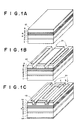
- a semiconductor laser device according to a first embodiment of the present invention will hereinafter be described along the fabrication process. Said fabrication process is shown in Figs. 1A-1C.
- an n-GaAs buffer layer 2 an n-Al 0.65 Ga 0.35 As lower cladding layer 3, an n- or i-In 0.5 Ga 0.5 P lower optical waveguide layer 4, an In 0.12 Ga 0.88 As 0.75 P 0.25 quantum well active layer 5, a p- or i-In 0.5 Ga 0.5 P upper optical waveguide layer 6, a p-Al 0.65 Ga 0.35 As first upper cladding layer 7, a p-or i-In 0.5 Ga 0.5 P etch-stopping layer 8, a p-Al 0.65 Ga 0.35 As second upper cladding layer 9, and a p-GaAs contact layer 10, are grown epitaxially upon a (1.0.0)-plane n-GaAs substrate 1 by organometallic vapor phase epitaxy.
- the first upper cladding layer 7 is grown to a thickness such that an index guide wave can reach a high output at the waveguide in the groove of the center portion of the resonator
- a photoresist film (not shown) is coated on the wafer, and a pre-exposure baking process (typically at 80 to 100°C) is performed in a hot plate for 1.
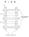
- the wafer coated with the photoresist film is irradiated with an exposure of 100 mJ through a mask in which grooves 21 of 10 ⁇ m in width are formed with a space of 50 ⁇ m (see Fig. 2)so that they are parallel to the original flat plane of the (1.0.0)-plane substrate 1 and perpendicular to the laser cleavage plane.
- the irradiated regions of the photoresist film are dissolved in a developing solution, and windows are formed in the photoresist film.
- the p-GaAs contact layer 10 and the p-Al 0.65 Ga 0.35 As second upper cladding layer 9 are etched to form the grooves 21 with a tartaric etchant.
- the etching is automatically stopped at the InGaP etch-stopping layer 8.
- a photomask to expose non-injection regions 31 is aligned with the wafer so that the non-injection regions 31 are evenly disposed on the end-face cleavage lines and the separation cleavage lines of the device.
- the wafer is irradiated with an exposure of 100 mJ.
- the irradiated regions of the photoresist film are dissolved in a developing solution, and the non-injection regions 31 are formed in the photoresist film.
- the wafer is immersed for 10 seconds in a mixed water solution with a 1:50 volume ratio of NH 3 :H 2 O 2 at room temperature, and portions of the p-GaAs contact layer 10 corresponding to the non-injection regions 31 are selectively etched.
- the p-GaAs contact layer 10 is etched, the side face of the p-GaAs contact layer 10 exposed to the groove 21 is situated inside the top edge of the groove 21.
- the photoresist film is dissolved in organic lye.
- a 150-nm SiO 2 insulating film 12 is formed by a plasma-assisted chemical vapor deposition (PCVD) apparatus. Since the side face of the p-GaAs contact layer 10 exposed to the groove 21 is situated inside the top edge of the groove 21, coverage by the insulating film 12 becomes satisfactory.
- a photoresist film is coated on the SiO 2 insulating film 12, and a photomask, having a window in a region 3 ⁇ m (indicated by a in the figure) away from the transverse edge of the 50- ⁇ m-wide ridge portion and 3 ⁇ m (indicated by b in the figure) away from the longitudinal edge of the ridge portion, is stacked on the wafer.
- the side face of the p-GaAs contact layer 10 exposed to the groove 21 is situated inside the top edge of the groove 21. Therefore, similarly, coverage by the p-electrode 13 (which is stacked on the SiO 2 insulating film 12) becomes satisfactory.
- the substrate 1 is polished and an n-electrode 14 is formed on the bottom surface of the substrate 1.
- the wafer is cleaved at both-end-face setting positions (end-face cleavage lines shown in Fig. 2) to form a plurality of laser array bars.
- the resonator end faces of each laser array bar are provided with a high reflective coating and a low reflective coating, respectively.
- the laser array bar is cleaved along the device-separation cleavage lines (see Fig. 2) into laser devices, and each laser device is bonded on a heat sink with an In (indium) soldering material so that the p-plane of the device contacts the heat sink.
- the semiconductor laser device of the first embodiment a portion of the contact layer 10 on the perimeter of the device has been removed.
- the insulating film 12 is peeled off as the laser array bar is cleaved. Even if the current conduction between the heat sink and the insulating film 12 occurs in the peeled region through the soldering material, when the p-plane of the device is bonded to the heat sink with the junction down, ohmic contact is not made and therefore no current flows, because the contact layer 10 has been removed.
- a n-type GaAs substrate has been employed.
- a p-type conductive substrate may be employed.
- the conductivity of each layer is reversed.
- a molecular beam epitaxial growth method employing solid matter or gas may be employed.
- the width (light-emitting width) of the ridge portion is not limited to 50 ⁇ m, but may be any width. Also, the width of the U-shaped groove 21 is not limited to 10 ⁇ m. For example, the U-shaped groove 21 may be a straight-walled groove so that the maximum width is obtained.
- the non-injection region i.e., a region from which the contact layer 10 is removed
- the non-injection region does not have to be formed along the perimeter of the device, as shown in the first embodiment. It may be formed only in a light-emitting region (ridge portion), or may be formed in one end face, not both end faces.
- the insulating film 12 may be formed by a deposition method other than a PCVD method.
- the material is not limited to SiO 2 . Any insulating material can be employed if it has processability. For instance, SiN may be employed. In the case of SiN, the film quality is finer and therefore leakage current due to defects can be reduced. As a result, an enhancement in throughput is expected.
- the p-electrode 13 has not been formed in the non-injection region. However, since the insulating film 12 is formed in the non-injection region, there is no possibility that current will be injected. Therefore, the p-electrode 13 may be formed on the insulating film 12.
- a semiconductor laser device according to a second embodiment of the present invention will hereinafter be described along the fabrication method.
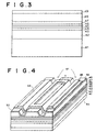
- a sectional view thereof up to the contact layer is shown in Fig. 3, and a perspective view thereof after electrode formation is shown in Fig. 4.
- the upper and lower optical waveguide layers 43, 47 are 0.4 ⁇ m in thickness.
- a photoresist film (not shown) is coated on the wafer, and a pre-exposure baking process (typically at 80 to 100°C) is performed in a hot plate for 1.
- Ultraviolet rays are irradiated to the photoresist film on the wafer with an exposure of 100 mJ through a mask such that grooves 61 of 10 ⁇ m in width are formed with a space of 50 ⁇ m so that they are parallel to the original flat plane of the (1.0.0)-plane substrate 41 and perpendicular to the laser cleavage plane.
- the irradiated regions of the photoresist film are dissolved in a developing solution, and windows are formed in the photoresist film.
- the p-GaAs contact layer 49 and the Ga 0.39 Al 0.61 As cladding layer 9 are etched to form the grooves 61 with a tartaric etchant.
- a photomask for exposing portions of the photoresist film near the device end faces which are to become current non-injection regions, is aligned with the wafer so that the non-injection regions are disposed on the device end-face cleavage lines (see Fig 2).
- the wafer is irradiated with an exposure of 100 mJ.
- the irradiated regions of the photoresist film are dissolved in a developing solution, and the non-injection regions are formed in the photoresist film.
- the wafer is immersed for 10 seconds in a mixed water solution with a 1:50 volume ratio of NH 3 :H 2 O 2 at room temperature, and portions of the p-GaAs contact layer 49 corresponding to the non-injection regions are selectively etched to form current non-injection portions.
- a 150-nm SiO 2 insulating film 52 is formed by plasma-assisted chemical vapor deposition (PCVD).
- PCVD plasma-assisted chemical vapor deposition
- a photoresist film is coated on the SiO 2 insulating film 52, and a photomask, having a window in a region 3 ⁇ m (indicated by a in Fig. 4) away from the transverse edge of the 50- ⁇ m-wide ridge portion and 3 ⁇ m (indicated by b in Fig. 4) away from the longitudinal edge of the ridge portion, is stacked on the wafer.
- a photomask having a window in a region 3 ⁇ m (indicated by a in Fig. 4) away from the transverse edge of the 50- ⁇ m-wide ridge portion and 3 ⁇ m (indicated by b in Fig. 4) away from the longitudinal edge of the ridge portion, is stacked on the wafer.
- ultraviolet rays are irradiated with an exposure of 100 mJ.
- the irradiated region of the photoresist film is dissolved in a developing solution to form the window.
- the photoresist film is dissolved in organic lye.
- a p-electrode 53 is formed in a region other than the non-injection regions.
- the substrate 41 is polished and an n-electrode 54 is formed on the bottom surface of the substrate 41.
- the thus-fabricated wafer is cleaved into laser array bars having a transverse length (resonator length) of 1.5 mm and a longitudinal length of 10 to 20 mm so that the (1.0.0) plane is exposed to the air.
- the optical resonator end faces of each laser array bar are exposed.
- One of the two end faces is coated with a film employing Al 2 O 3 so that it has a thickness equivalent to a reflection ratio of 6 ⁇ 1% (emission wavelength 809 nm).
- the other of the two end faces has a stacked structure of ⁇ /4 oxide (e.g., Al 2 O 3 /TiO 2 /(SiO 2 /TiO 2 ) 4 : Al 2 O 3 , TiO 2 , SiO 2 , TiO 2 , SiO 2 , TiO 2 , SiO 2 , TiO 2 , SiO 2 , and TiO 2 are stacked in the recited order from the cleavage plane), and the reflection ratio is 95% or greater.
- ⁇ /4 oxide e.g., Al 2 O 3 /TiO 2 /(SiO 2 /TiO 2 ) 4 : Al 2 O 3 , TiO 2 , SiO 2 , TiO 2 , SiO 2 , TiO 2 , SiO 2 , TiO 2 , SiO 2 , and TiO 2 are stacked in the recited order from the cleavage plane), and the reflection ratio is 95% or greater.
- the laser array bar with the reflection-ratio control layers is cleaved into semiconductor laser devices at intervals of 500 to 600 ⁇ m so that each laser device has a transverse length of 500 to 600 ⁇ m and a longitudinal length (resonator length) of 1.5 mm.
- the aforementioned semiconductor laser device is bonded on a heat sink.
- the entire surface (Cu) of the heat sink is plated with Ni (thickness 5 ⁇ m).
- Ni (50 to 150 nm), Pt (50 to 200 nm), and In (3.5 to 5.5 ⁇ m) are deposited in the recited order so that the area is at least 4 times the device area.
- This heat sink is heated in a temperature range of 180 to 220°C to melt In (indium), and the p-plane of the device is bonded on the melted In.
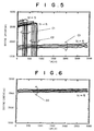
- the time-lapse reliability of the semiconductor laser device fabricated in the aforementioned manner was evaluated.
- the results of evaluation are shown in Figs. 5 and 6.
- the results are shown by C3 in Fig. 5.
- the same device was tested at an environmental temperature of 60°C with an output of 2.0 W.
- the results are shown by C2 in Fig. 5.
- a device, which has an end-face current non-injection structure without the tensile strain barrier layer of the aforementioned semiconductor laser device was tested at an environmental temperature of 60°C with an output of 2.0 W.
- the results are shown by C1 in Fig. 5.
- the aforementioned semiconductor laser device of the present invention provided with the tensile strain barrier layer and the end-face current non-injection region, was tested at an environmental temperature of 60°C with an output of 2.0 W. The results are shown by C4 in Fig. 6. For each level, five devices were tested.
- the device with the tensile strain barrier layer and without the end-face current non-injection structure operates for about 3000 hours with an output of 1.5 W. However, if the output is increased to 2.0 W, the operation of the device ceases to operate after approximately 600 to 800 hours, as shown by C2 in Fig. 5. In addition, as shown by C1, in the device with the end-face current non-injection structure and without the tensile strain barrier layer, the operation ceases betweenafter approximately 250 to 450 hours. Compared with these results, it is found, as shown by C4 in Fig. 6, that the device of the present invention with the tensile strain barrier layer and the end-face current non-injection structure operates for about 3000 hours with an output of 2.0 W.
- the step of forming grooves and the step of removing a portion of the contact layer to form a current non-injection region must be performed, and consequently, there is a problem that the steps will be troublesome and time-consuming.
- the photoresist material, applied by spin coating is formed thicker in the etching grooves than on the flat portions and is hardened by an NH 3 :H 2 O 2 mixed water solution that selectively etches the contact layer.
- the semiconductor laser device of the third embodiment as with the semiconductor laser device of the first embodiment, has a ridge structure in which grooves are formed in the p-type contact layer and the cladding layer underneath the contact layer. Therefore, a description will be made only of the layer structure.
- each cladding layer and each optical waveguide layer have composition ratios which have a lattice match with respect to the GaAs substrate, respectively.
- a p-InGaP etch-stopping layer with a thickness of 10 nm may be provided anywhere in the p-Ga 1-z1 Al z1 As cladding layer.
- the n-type GaAs substrate has been employed.
- a p-type conductive substrate may be employed.
- the conductivity of each layer is reversed.
- a molecular beam epitaxial growth method employing solid matter or gas may be employed.
- the width (light-emitting width) of the ridge portion is not limited to 50 ⁇ m, but may be any width. Also, the width of the U-shaped groove 61 is not limited to 10 ⁇ m. For example, the U-shaped groove 61 may be a straight-walled groove so that the maximum width is obtained.
- the area of the current non-injection region is between 5 ⁇ m and 50 ⁇ m from the cleavage plane. If the range is less than 5 ⁇ m, it is extremely difficult to form the current non-injection region because of spreading of current caused by the second conduction-type GaAs contact layer. As a result, end-face degradation occurs due to generation of heat. If it is greater than 50 ⁇ m, the current non-injection region absorbs light and increases light loss, resulting in a reduction in the light output.
- the non-injection region does not have to be formed along the perimeter of the device. It may be provided only on the light-emitting region (ridge portion), or may be provided on only one of the end-faces (light-exit end face), not both.
- the insulating film 52 may be formed by a deposition method other than a PCVD method.
- the material is not limited to SiO 2 . Any insulating material can be employed if it has processability.
- a solid-state laser apparatus with the semiconductor laser device of the first embodiment as its excitation light source will hereinafter be described with reference to Fig. 7.
- the solid-state laser apparatus is a solid-state laser apparatus making use of second harmonic generation.
- the high-output semiconductor laser device 71 of the first embodiment mounted on a heat sink 70 is used as an excitation light source.
- the solid-state laser apparatus further comprises a lens 72 for collecting excitation light emitted from the semiconductor laser device 71, a solid-state laser crystal 73 in which laser emission is performed by the collected excitation light, and an output mirror 74, consisting of a concave mirror, which forms a solid-state laser resonator along with the solid-state laser crystal 73.
- the solid-state laser crystal 73 has a coating 76 on the semiconductor laser device side.
- the coating 76 is highly reflective with respect to light emitted from the solid-state laser crystal 73 and is reflectionless with respect to light emitted from the semiconductor laser device 71.
- the solid-state laser resonator is formed by the output mirror 74, which consists of a concave mirror, and the coating 76.
- a KNbO3 non-linear crystal 75 for reducing the wavelength of the laser light emitted from the solid-state laser crystal 73 to one half and then generating a second harmonic.
- the solid-state laser crystal 73 may employ Nb:YVO 4 , etc.
- the nonlinear crystal 75 may employ KTP, etc.
- the temperatures of the semiconductor laser device 71, the solid-state laser crystal 73, and the non-linear crystal 75 are controlled by a Peltier element (not shown).
- APC automatic power control
- the semiconductor laser device of the present invention can be used as an array-type semiconductor laser device in addition to the excitation light source of the solid-state laser apparatus of the present invention, and can be mounted on an integrated circuit, etc.
- the semiconductor laser device and the solid-state laser apparatus of the present invention are capable of emitting laser light whose reliability is high from a low output to a high output. Because of high reliability, they can be used in array-type semiconductor lasers and integrated circuits. In addition, they are applicable as light sources in many areas of high-speed information and image processing, optical communication, optical measuring, medical treatment, and laser printing.
Landscapes
- Physics & Mathematics (AREA)
- Optics & Photonics (AREA)
- Condensed Matter Physics & Semiconductors (AREA)
- General Physics & Mathematics (AREA)
- Electromagnetism (AREA)
- Engineering & Computer Science (AREA)
- Chemical & Material Sciences (AREA)
- Nanotechnology (AREA)
- Life Sciences & Earth Sciences (AREA)
- Biophysics (AREA)
- Geometry (AREA)
- Crystallography & Structural Chemistry (AREA)
- Semiconductor Lasers (AREA)
Abstract
Description
Claims (17)
- A semiconductor laser device comprising:a substrate, a semiconductor layer including an active layer, a cladding layer, and a contact layer stacked in the recited order;two exposed portions having a depth at which said semiconductor layer is exposed continuously from one of two resonator end faces to the other; anda ridge portion, formed between said two exposed portions, which has a current injection window;
wherein in at least one of the resonator end faces of said ridge portion, a portion of said contact layer near said one resonator end face is removed;an insulating film is formed so that it covers a region, excluding said current injection window, of said contact layer, and portions of said cladding layer exposed by removing the portion of said contact layer near said one resonator end face; andan electrode is formed on at least a portion of said contact layer exposed to said current injection window. - The semiconductor laser device as set forth in claim 1, wherein the uppermost layer of said semiconductor layer in a stacking direction is an etch-stopping layer, said cladding layer is provided on said etch-stopping layer, and a layer exposed to the bottom portions of said two exposed portions is said etch-stopping layer.
- The semiconductor laser device as set forth in claim 1, wherein said cladding layer comprises AlGaAs and said contact layer comprises GaAs.
- The semiconductor laser device as set forth in claim 2, wherein said cladding layer comprises AlGaAs and said contact layer comprises GaAs.
- The semiconductor laser device as set forth in claim 2, wherein said etch-stopping layer comprises InGaP.
- The semiconductor laser device as set forth in claim 2, wherein said cladding layer comprises AlGaAs, said contact layer comprises GaAs, and said etch-stopping layer comprises InGaP.
- The semiconductor laser device as set forth in claim 2, wherein another cladding layer is provided underneath said etch-stopping layer, is the same in conductivity and nearly the same in refractive index as said cladding layer, and has a lattice match with respect to said substrate.
- The semiconductor laser device as set forth in claim 1, wherein a side face of said contact layer exposed to said exposed portion is situated inside an edge of a top surface of said cladding layer exposed to said exposed portion.
- The semiconductor laser device as set forth in claim 1, wherein the portion of said contact layer near said resonator end face, which is removed, is in a range between 5 µm and 50 µm, from said one resonator end face.
- A method of fabricating a semiconductor laser device, comprising the steps of:stacking a cladding layer and a contact layer on a semiconductor layer including an active layer, in the recited order;forming a photoresist film, which has two windows extending from one of two resonator end faces to the other, on said contact layer through a mask, and then etching said cladding layer and said contact layer to form two grooves, corresponding to said two windows, and a ridge portion between said two grooves;forming a window in at least a portion of said photoresist film near one of the two resonator end faces of said ridge portion through a mask, and then selectively etching and removing a portion of said contact layer which is near said one resonator end face; andlifting off and removing said photoresist film.
- The method as set forth in claim 10, wherein said cladding layer comprises AlGaAs, said contact layer comprises GaAs, and said contact layer is etched with an NH3:H2O2 mixed water solution.
- A semiconductor laser device comprising:two opposite resonator end faces where at least a first conduction type first cladding layer, a first conduction type or i-type first optical waveguide layer, an i-type Inx2Ga1- x2As1-y2Py2 first barrier layer having tensile strain (where x2/0.49≦y2≦0.3+(x2/0.49), and 0.8≦y2≦1.0), an i-type Inx3Ga1-x3As1-y3Py quantum well active layer (where 0.3≦x3≦0.2 and y3=x3/0.49), an i-type Inx2Ga1-x2As1-y2Py2 second barrier layer having tensile strain (where x2/0.49≦y2≦0.3+(x2/0.49), and 0.8≦y2≦1.0), a second conduction type or i-type second optical waveguide layer, a second conduction type second cladding layer, a second conduction type contact layer, are stacked on a first conduction type GaAs substrate in the recited order;wherein said first cladding layer and said second cladding layer comprise compositions which have a lattice match with respect to said GaAs substrate, respectively;said first optical waveguide layer and said second optical waveguide layer comprise compositions which have a lattice match with respect to said GaAs substrate, respectively;the total thickness of said first barrier layer and said second barrier layer is between 10 nm and 30 nm;said first barrier layer and said second barrier layer have tensile strains with respect to said GaAs substrate, respectively, and comprise a composition in which the product of a tensile strain quantity common to said two barrier layers and said total thickness is between 0.05 nm and 0.2 nm;said quantum well active layer comprises a composition which has a lattice match with respect to said GaAs substrate or composition which has a tensile strain of - 0.007 with respect to said substrate; anda current non-injection region is provided near at least one of said two opposite resonator end faces.
- The semiconductor laser device as set forth in claim 12, whereinsaid current non-injection region is formed by removing at least a portion of said contact layer that is near said one resonator end face;an insulating film is formed from the remaining contact layer on said second cladding layer to said second cladding layer exposed to said current non-injection region, a current injection window is formed by removing a portion of said insulating film to inject current; andan electrode is formed on a portion of said insulating film other than said current non-injection region so that it covers at least said current injection window.
- The semiconductor laser device as set forth in claim 12, wherein said contact layer comprises GaAs and said cladding layer has a composition that is not etched by an etchant for GaAs.
- The semiconductor laser device as set forth in claim 13, wherein said contact layer comprises GaAs and said cladding layer has a composition that is not etched by an etchant for GaAs.
- The semiconductor laser device as set forth in claim 12, wherein said current non-injection region is formed in a range between 5 µm and 50 µm, from said resonator end face.
- A solid-state laser apparatus comprising:wherein said excitation light source comprises the semiconductor laser device as set forth in claim 1 or 12.an excitation light source; anda solid-state laser crystal for emitting laser light by being excited with excitation light emitted from said excitation light source;
Priority Applications (1)
| Application Number | Priority Date | Filing Date | Title |
|---|---|---|---|
| EP05012544A EP1583187B1 (en) | 2000-10-12 | 2001-10-11 | Semiconductor laser device with a current non-injection region near a resonator end face |
Applications Claiming Priority (6)
| Application Number | Priority Date | Filing Date | Title |
|---|---|---|---|
| JP2000311405 | 2000-10-12 | ||
| JP2000311405 | 2000-10-12 | ||
| JP2000360432 | 2000-11-28 | ||
| JP2000360432A JP2002164618A (en) | 2000-11-28 | 2000-11-28 | Semiconductor laser device |
| JP2001038689A JP2002190644A (en) | 2000-10-12 | 2001-02-15 | Semiconductor laser element and method of manufacturing the same |
| JP2001038689 | 2001-02-15 |
Related Child Applications (1)
| Application Number | Title | Priority Date | Filing Date |
|---|---|---|---|
| EP05012544A Division EP1583187B1 (en) | 2000-10-12 | 2001-10-11 | Semiconductor laser device with a current non-injection region near a resonator end face |
Publications (3)
| Publication Number | Publication Date |
|---|---|
| EP1198042A2 true EP1198042A2 (en) | 2002-04-17 |
| EP1198042A3 EP1198042A3 (en) | 2004-04-28 |
| EP1198042B1 EP1198042B1 (en) | 2006-05-10 |
Family
ID=27344912
Family Applications (2)
| Application Number | Title | Priority Date | Filing Date |
|---|---|---|---|
| EP05012544A Expired - Lifetime EP1583187B1 (en) | 2000-10-12 | 2001-10-11 | Semiconductor laser device with a current non-injection region near a resonator end face |
| EP01124461A Expired - Lifetime EP1198042B1 (en) | 2000-10-12 | 2001-10-11 | Semiconductor laser device with a current non-injection region near a resonator end face, and fabrication method thereof |
Family Applications Before (1)
| Application Number | Title | Priority Date | Filing Date |
|---|---|---|---|
| EP05012544A Expired - Lifetime EP1583187B1 (en) | 2000-10-12 | 2001-10-11 | Semiconductor laser device with a current non-injection region near a resonator end face |
Country Status (3)
| Country | Link |
|---|---|
| US (2) | US6888866B2 (en) |
| EP (2) | EP1583187B1 (en) |
| DE (2) | DE60129261T2 (en) |
Cited By (3)
| Publication number | Priority date | Publication date | Assignee | Title |
|---|---|---|---|---|
| US6678303B2 (en) * | 2001-06-22 | 2004-01-13 | Fuji Photo Film Co., Ltd. | Semiconductor laser device in which end of electric-to-optical conversion layer protrudes outward from shortest current path between end facets of cladding layers |
| EP1840978A4 (en) * | 2005-01-17 | 2014-06-25 | Anritsu Corp | SEMICONDUCTOR OPTICAL ELEMENT HAVING OPTICAL LARGE SPECTRUM TRANSMISSION CHARACTERISTICS, METHOD FOR MANUFACTURING THE SAME, AND EXTERNAL RESONATOR TYPE SEMICONDUCTOR LASER |
| CN110764185A (en) * | 2019-10-12 | 2020-02-07 | 天津大学 | A kind of preparation method of low-loss lithium niobate thin film optical waveguide |
Families Citing this family (21)
| Publication number | Priority date | Publication date | Assignee | Title |
|---|---|---|---|---|
| JP4504610B2 (en) * | 2002-03-01 | 2010-07-14 | 株式会社日立製作所 | Ridge type semiconductor laser device |
| JP2003273464A (en) * | 2002-03-19 | 2003-09-26 | Mitsubishi Electric Corp | Ridge waveguide type semiconductor laser device |
| JP4480948B2 (en) * | 2002-07-15 | 2010-06-16 | 日本オプネクスト株式会社 | Semiconductor laser device and manufacturing method thereof |
| JP2004158615A (en) * | 2002-11-06 | 2004-06-03 | Mitsubishi Electric Corp | Semiconductor laser device |
| JP4472278B2 (en) * | 2003-06-26 | 2010-06-02 | 三菱電機株式会社 | Semiconductor laser element |
| JP2005033021A (en) * | 2003-07-04 | 2005-02-03 | Sumitomo Electric Ind Ltd | Semiconductor optical device and manufacturing method thereof |
| JP2005158800A (en) * | 2003-11-20 | 2005-06-16 | Sharp Corp | Manufacturing method of semiconductor device and semiconductor device manufactured by the manufacturing method |
| JP2006148032A (en) * | 2004-11-25 | 2006-06-08 | Toshiba Corp | Semiconductor laser device |
| CN105207053B (en) | 2005-02-18 | 2019-06-04 | 镁可微波技术有限公司 | High reliability etched facet photonic devices |
| JP2006303299A (en) * | 2005-04-22 | 2006-11-02 | Sharp Corp | Semiconductor laser |
| KR100764393B1 (en) * | 2006-02-22 | 2007-10-05 | 삼성전기주식회사 | Manufacturing method of high output array type semiconductor laser device |
| US20120223354A1 (en) * | 2009-10-18 | 2012-09-06 | Technion-Research & Development Foundation | Semiconductor two-photo device |
| US8571080B2 (en) * | 2009-12-02 | 2013-10-29 | Massachusetts Institute Of Technology | High efficiency slab-coupled optical waveguide laser and amplifier |
| RU2549553C2 (en) * | 2013-07-30 | 2015-04-27 | Общество с ограниченной ответственностью "Новолюм" | Injection laser |
| RU2557359C2 (en) * | 2013-10-09 | 2015-07-20 | Федеральное государственное бюджетное учреждение науки Физико-технический институт им. А.Ф. Иоффе Российской академии наук | Laser-thyristor |
| JP7121536B2 (en) * | 2018-05-18 | 2022-08-18 | 株式会社堀場製作所 | Semiconductor laser device manufacturing method, semiconductor laser device therefor, and gas analysis device |
| WO2020142292A1 (en) * | 2018-12-31 | 2020-07-09 | Nlight, Inc. | Method, system, apparatus for differential current injection |
| WO2020204053A1 (en) * | 2019-04-02 | 2020-10-08 | パナソニックセミコンダクターソリューションズ株式会社 | Semiconductor laser device |
| CN116746012A (en) * | 2021-01-29 | 2023-09-12 | 新唐科技日本株式会社 | Semiconductor laser components |
| CN113345808B (en) * | 2021-08-05 | 2021-10-29 | 度亘激光技术(苏州)有限公司 | A method of bonding a semiconductor device and a heat sink |
| CN117154533A (en) * | 2022-05-11 | 2023-12-01 | 武汉光迅科技股份有限公司 | An InP-based semiconductor laser chip and preparation method |
Family Cites Families (20)
| Publication number | Priority date | Publication date | Assignee | Title |
|---|---|---|---|---|
| JPS54115088A (en) * | 1978-02-28 | 1979-09-07 | Nec Corp | Double hetero junction laser element of stripe type |
| US4371966A (en) * | 1980-11-06 | 1983-02-01 | Xerox Corporation | Heterostructure lasers with combination active strip and passive waveguide strip |
| US4620308A (en) | 1985-10-30 | 1986-10-28 | Lectromelt Corporation | Arc furnace electrode control |
| JPS6338279A (en) | 1986-08-04 | 1988-02-18 | Sharp Corp | Manufacture of semiconductor device |
| JPH03222488A (en) * | 1990-01-29 | 1991-10-01 | Furukawa Electric Co Ltd:The | Semiconductor laser element and manufacture thereof |
| JPH05327112A (en) | 1992-05-20 | 1993-12-10 | Sanyo Electric Co Ltd | Manufacture of semiconductor laser |
| US5394421A (en) * | 1993-01-11 | 1995-02-28 | Rohm Co., Ltd. | Semiconductor laser device including a step electrode in a form of eaves |
| JPH09298340A (en) | 1996-04-30 | 1997-11-18 | Fuji Photo Film Co Ltd | Laser light emitting equipment using semiconductor laser |
| JPH10163563A (en) | 1996-11-29 | 1998-06-19 | Furukawa Electric Co Ltd:The | Semiconductor laser |
| JPH10233556A (en) * | 1997-02-20 | 1998-09-02 | Mitsubishi Electric Corp | Ridge type semiconductor laser diode and method of manufacturing the same |
| KR100243417B1 (en) * | 1997-09-29 | 2000-02-01 | 이계철 | High power semiconductor laser with Al double holding structure |
| JP3753216B2 (en) | 1997-11-25 | 2006-03-08 | 富士写真フイルム株式会社 | Semiconductor laser device |
| JP3317335B2 (en) * | 1998-02-10 | 2002-08-26 | 富士写真フイルム株式会社 | Semiconductor laser device |
| JPH11354880A (en) | 1998-06-03 | 1999-12-24 | Rohm Co Ltd | Semiconductor laser element and its manufacturing method |
| JP2000101198A (en) * | 1998-09-18 | 2000-04-07 | Fuji Photo Film Co Ltd | Semiconductor laser |
| US6400743B1 (en) * | 1999-08-05 | 2002-06-04 | Fuji Photo Film Co., Ltd. | High-power semiconductor laser device having current confinement structure and index-guided structure |
| JP2001053384A (en) * | 1999-08-05 | 2001-02-23 | Fuji Photo Film Co Ltd | Semiconductor laser device and method of manufacturing the same |
| DE60021505T2 (en) * | 1999-11-19 | 2006-06-01 | Fuji Photo Film Co. Ltd., Minamiashigara | High-power semiconductor laser with current limitation and index-guided structure |
| US6580738B2 (en) * | 1999-12-08 | 2003-06-17 | Fuji Photo Film Co., Ltd. | High-power semiconductor laser device in which near-edge portions of active layer are removed |
| JP2002141610A (en) * | 2000-10-31 | 2002-05-17 | Fuji Photo Film Co Ltd | Semiconductor laser element and its fabricating method |
-
2001
- 2001-10-11 EP EP05012544A patent/EP1583187B1/en not_active Expired - Lifetime
- 2001-10-11 US US09/973,814 patent/US6888866B2/en not_active Expired - Lifetime
- 2001-10-11 DE DE60129261T patent/DE60129261T2/en not_active Expired - Lifetime
- 2001-10-11 EP EP01124461A patent/EP1198042B1/en not_active Expired - Lifetime
- 2001-10-11 DE DE60119470T patent/DE60119470T2/en not_active Expired - Lifetime
-
2005
- 2005-03-11 US US11/076,918 patent/US20050164420A1/en not_active Abandoned
Cited By (4)
| Publication number | Priority date | Publication date | Assignee | Title |
|---|---|---|---|---|
| US6678303B2 (en) * | 2001-06-22 | 2004-01-13 | Fuji Photo Film Co., Ltd. | Semiconductor laser device in which end of electric-to-optical conversion layer protrudes outward from shortest current path between end facets of cladding layers |
| EP1840978A4 (en) * | 2005-01-17 | 2014-06-25 | Anritsu Corp | SEMICONDUCTOR OPTICAL ELEMENT HAVING OPTICAL LARGE SPECTRUM TRANSMISSION CHARACTERISTICS, METHOD FOR MANUFACTURING THE SAME, AND EXTERNAL RESONATOR TYPE SEMICONDUCTOR LASER |
| CN110764185A (en) * | 2019-10-12 | 2020-02-07 | 天津大学 | A kind of preparation method of low-loss lithium niobate thin film optical waveguide |
| CN110764185B (en) * | 2019-10-12 | 2021-01-01 | 天津大学 | A kind of preparation method of low-loss lithium niobate thin film optical waveguide |
Also Published As
| Publication number | Publication date |
|---|---|
| DE60119470D1 (en) | 2006-06-14 |
| US6888866B2 (en) | 2005-05-03 |
| DE60129261D1 (en) | 2007-08-16 |
| EP1583187B1 (en) | 2007-07-04 |
| US20020061044A1 (en) | 2002-05-23 |
| EP1198042B1 (en) | 2006-05-10 |
| DE60129261T2 (en) | 2008-05-08 |
| US20050164420A1 (en) | 2005-07-28 |
| EP1583187A1 (en) | 2005-10-05 |
| DE60119470T2 (en) | 2007-04-19 |
| EP1198042A3 (en) | 2004-04-28 |
Similar Documents
| Publication | Publication Date | Title |
|---|---|---|
| EP1198042B1 (en) | Semiconductor laser device with a current non-injection region near a resonator end face, and fabrication method thereof | |
| US5386428A (en) | Stacked active region laser array for multicolor emissions | |
| EP1437809B1 (en) | Compound semiconductor laser | |
| US20130301667A1 (en) | Semiconductor laser device and manufacturing method of the same | |
| US6744797B2 (en) | Semiconductor laser device | |
| EP1104057B1 (en) | High-power semiconductor laser device having current confinement structure and index-guided structure | |
| EP0789430B1 (en) | A method of producing a semiconductor laser device | |
| EP0939471A1 (en) | Vertical-cavity surface-emitting semiconductor laser | |
| US4769821A (en) | High power semiconductor laser by means of lattice mismatch stress | |
| US6541291B2 (en) | Semiconductor light emitting device in which near-edge portion is filled with doped regrowth layer, and dopant to regrowth layer is diffused into near-edge region of active layer | |
| US6567444B2 (en) | High-power semiconductor laser device in which near-edge portions of active layer are removed | |
| JP2005286192A (en) | Optical integrated device | |
| US20080298412A1 (en) | Semiconductor laser device and manufacturing method thereof | |
| US6621845B2 (en) | Semiconductor laser device which includes AlGaAs optical waveguide layer being formed over internal stripe groove and having controlled refractive index | |
| US6625190B1 (en) | Semiconductor laser device having thickened impurity-doped aluminum-free optical waveguide layers | |
| CN115411617B (en) | Vertical cavity surface emitting laser and preparation method thereof | |
| US6707834B2 (en) | Semiconductor laser device and process for producing the same | |
| JPH10261835A (en) | Semiconductor laser device and method of manufacturing the same | |
| JP4033930B2 (en) | Semiconductor laser | |
| CN115189225B (en) | A laser chip with improved reliability and its fabrication process | |
| EP0427003A1 (en) | Semiconductor light-emitting element and its manufacturing method | |
| JPH06252448A (en) | Semiconductor light emitting device and manufacture thereof | |
| JP2002190644A (en) | Semiconductor laser element and method of manufacturing the same | |
| KR101028262B1 (en) | Semiconductor laser diode and manufacturing method thereof | |
| JPH11284272A (en) | Semiconductor laser device and method of manufacturing the same |
Legal Events
| Date | Code | Title | Description |
|---|---|---|---|
| PUAI | Public reference made under article 153(3) epc to a published international application that has entered the european phase |
Free format text: ORIGINAL CODE: 0009012 |
|
| AK | Designated contracting states |
Kind code of ref document: A2 Designated state(s): AT BE CH CY DE DK ES FI FR GB GR IE IT LI LU MC NL PT SE TR |
|
| AX | Request for extension of the european patent |
Free format text: AL;LT;LV;MK;RO;SI |
|
| PUAL | Search report despatched |
Free format text: ORIGINAL CODE: 0009013 |
|
| AK | Designated contracting states |
Kind code of ref document: A3 Designated state(s): AT BE CH CY DE DK ES FI FR GB GR IE IT LI LU MC NL PT SE TR |
|
| AX | Request for extension of the european patent |
Extension state: AL LT LV MK RO SI |
|
| 17P | Request for examination filed |
Effective date: 20041020 |
|
| 17Q | First examination report despatched |
Effective date: 20041116 |
|
| AKX | Designation fees paid |
Designated state(s): CH DE FR GB LI |
|
| GRAP | Despatch of communication of intention to grant a patent |
Free format text: ORIGINAL CODE: EPIDOSNIGR1 |
|
| GRAS | Grant fee paid |
Free format text: ORIGINAL CODE: EPIDOSNIGR3 |
|
| GRAA | (expected) grant |
Free format text: ORIGINAL CODE: 0009210 |
|
| AK | Designated contracting states |
Kind code of ref document: B1 Designated state(s): CH DE FR GB LI |
|
| REG | Reference to a national code |
Ref country code: GB Ref legal event code: FG4D |
|
| REG | Reference to a national code |
Ref country code: CH Ref legal event code: EP |
|
| REF | Corresponds to: |
Ref document number: 60119470 Country of ref document: DE Date of ref document: 20060614 Kind code of ref document: P |
|
| REG | Reference to a national code |
Ref country code: CH Ref legal event code: NV Representative=s name: BOVARD AG PATENTANWAELTE |
|
| ET | Fr: translation filed | ||
| RAP2 | Party data changed (patent owner data changed or rights of a patent transferred) |
Owner name: FUJIFILM CORPORATION |
|
| PLBE | No opposition filed within time limit |
Free format text: ORIGINAL CODE: 0009261 |
|
| STAA | Information on the status of an ep patent application or granted ep patent |
Free format text: STATUS: NO OPPOSITION FILED WITHIN TIME LIMIT |
|
| REG | Reference to a national code |
Ref country code: GB Ref legal event code: 732E |
|
| 26N | No opposition filed |
Effective date: 20070213 |
|
| REG | Reference to a national code |
Ref country code: CH Ref legal event code: PUE Owner name: FUJIFILM CORPORATION Free format text: FUJI PHOTO FILM CO., LTD.#210 NAKANUMA,#MINAMI-ASHIGARA-SHI, KANAGAWA-KEN (JP) -TRANSFER TO- FUJIFILM CORPORATION#26-30, NISHIAZABU 2-CHOME MINATO-KU#TOKYO (JP) |
|
| REG | Reference to a national code |
Ref country code: FR Ref legal event code: CD Ref country code: FR Ref legal event code: TP |
|
| REG | Reference to a national code |
Ref country code: CH Ref legal event code: PFA Owner name: FUJIFILM CORPORATION Free format text: FUJIFILM CORPORATION#26-30, NISHIAZABU 2-CHOME MINATO-KU#TOKYO (JP) -TRANSFER TO- FUJIFILM CORPORATION#26-30, NISHIAZABU 2-CHOME MINATO-KU#TOKYO (JP) |
|
| REG | Reference to a national code |
Ref country code: CH Ref legal event code: PUE Owner name: NICHIA CORPORATION Free format text: FUJIFILM CORPORATION#26-30, NISHIAZABU 2-CHOME MINATO-KU#TOKYO (JP) -TRANSFER TO- NICHIA CORPORATION#491 OKA, KAMINAKA-CHO ANAN-SHI#TOKUSHIMA 774-8601 (JP) |
|
| REG | Reference to a national code |
Ref country code: DE Ref legal event code: R082 Ref document number: 60119470 Country of ref document: DE Representative=s name: KLUNKER, SCHMITT-NILSON, HIRSCH, DE |
|
| REG | Reference to a national code |
Ref country code: CH Ref legal event code: NV Representative=s name: BOVARD AG |
|
| REG | Reference to a national code |
Ref country code: DE Ref legal event code: R082 Ref document number: 60119470 Country of ref document: DE Representative=s name: KLUNKER, SCHMITT-NILSON, HIRSCH, DE Effective date: 20120521 Ref country code: DE Ref legal event code: R081 Ref document number: 60119470 Country of ref document: DE Owner name: NICHIA CORP., ANAN-SHI, JP Free format text: FORMER OWNER: FUJIFILM CORP., TOKIO/TOKYO, JP Effective date: 20120521 Ref country code: DE Ref legal event code: R082 Ref document number: 60119470 Country of ref document: DE Representative=s name: KLUNKER IP PATENTANWAELTE PARTG MBB, DE Effective date: 20120521 |
|
| REG | Reference to a national code |
Ref country code: GB Ref legal event code: 732E Free format text: REGISTERED BETWEEN 20120621 AND 20120627 |
|
| REG | Reference to a national code |
Ref country code: FR Ref legal event code: TP Owner name: NICHIA CORPORATION, JP Effective date: 20120806 |
|
| PGFP | Annual fee paid to national office [announced via postgrant information from national office to epo] |
Ref country code: FR Payment date: 20131009 Year of fee payment: 13 Ref country code: CH Payment date: 20131014 Year of fee payment: 13 |
|
| REG | Reference to a national code |
Ref country code: CH Ref legal event code: PL |
|
| PG25 | Lapsed in a contracting state [announced via postgrant information from national office to epo] |
Ref country code: LI Free format text: LAPSE BECAUSE OF NON-PAYMENT OF DUE FEES Effective date: 20141031 Ref country code: CH Free format text: LAPSE BECAUSE OF NON-PAYMENT OF DUE FEES Effective date: 20141031 |
|
| REG | Reference to a national code |
Ref country code: FR Ref legal event code: ST Effective date: 20150630 |
|
| PG25 | Lapsed in a contracting state [announced via postgrant information from national office to epo] |
Ref country code: FR Free format text: LAPSE BECAUSE OF NON-PAYMENT OF DUE FEES Effective date: 20141031 |
|
| REG | Reference to a national code |
Ref country code: DE Ref legal event code: R082 Ref document number: 60119470 Country of ref document: DE Representative=s name: KLUNKER IP PATENTANWAELTE PARTG MBB, DE |
|
| PGFP | Annual fee paid to national office [announced via postgrant information from national office to epo] |
Ref country code: DE Payment date: 20191001 Year of fee payment: 19 |
|
| PGFP | Annual fee paid to national office [announced via postgrant information from national office to epo] |
Ref country code: GB Payment date: 20191011 Year of fee payment: 19 |
|
| REG | Reference to a national code |
Ref country code: DE Ref legal event code: R119 Ref document number: 60119470 Country of ref document: DE |
|
| GBPC | Gb: european patent ceased through non-payment of renewal fee |
Effective date: 20201011 |
|
| PG25 | Lapsed in a contracting state [announced via postgrant information from national office to epo] |
Ref country code: DE Free format text: LAPSE BECAUSE OF NON-PAYMENT OF DUE FEES Effective date: 20210501 |
|
| PG25 | Lapsed in a contracting state [announced via postgrant information from national office to epo] |
Ref country code: GB Free format text: LAPSE BECAUSE OF NON-PAYMENT OF DUE FEES Effective date: 20201011 |