EP1195709A2 - IC contact unit and IC card reader - Google Patents
IC contact unit and IC card reader Download PDFInfo
- Publication number
- EP1195709A2 EP1195709A2 EP01308230A EP01308230A EP1195709A2 EP 1195709 A2 EP1195709 A2 EP 1195709A2 EP 01308230 A EP01308230 A EP 01308230A EP 01308230 A EP01308230 A EP 01308230A EP 1195709 A2 EP1195709 A2 EP 1195709A2
- Authority
- EP
- European Patent Office
- Prior art keywords
- card
- movable support
- contact
- contact unit
- actuator
- Prior art date
- Legal status (The legal status is an assumption and is not a legal conclusion. Google has not performed a legal analysis and makes no representation as to the accuracy of the status listed.)
- Granted
Links
Images





Classifications
-
- G—PHYSICS
- G06—COMPUTING OR CALCULATING; COUNTING
- G06K—GRAPHICAL DATA READING; PRESENTATION OF DATA; RECORD CARRIERS; HANDLING RECORD CARRIERS
- G06K13/00—Conveying record carriers from one station to another, e.g. from stack to punching mechanism
- G06K13/02—Conveying record carriers from one station to another, e.g. from stack to punching mechanism the record carrier having longitudinal dimension comparable with transverse dimension, e.g. punched card
- G06K13/08—Feeding or discharging cards
- G06K13/085—Feeding or discharging cards using an arrangement for locking the inserted card
-
- G—PHYSICS
- G06—COMPUTING OR CALCULATING; COUNTING
- G06K—GRAPHICAL DATA READING; PRESENTATION OF DATA; RECORD CARRIERS; HANDLING RECORD CARRIERS
- G06K13/00—Conveying record carriers from one station to another, e.g. from stack to punching mechanism
- G06K13/02—Conveying record carriers from one station to another, e.g. from stack to punching mechanism the record carrier having longitudinal dimension comparable with transverse dimension, e.g. punched card
- G06K13/08—Feeding or discharging cards
Definitions
- the present invention relates to an IC contact unit including a movable support provided with an IC contact point capable of coming in contact with a terminal of a magnetic IC card.
- an automatic transaction apparatus such as an automatic teller machine has a built-in IC card reader, and is structured such that customer data (fixed data) of an IC card is read by a magnetic head, and variable data such as transaction data is subjected to read/write processing by an IC contact unit.
- an IC contact unit in order to process the card data by bringing an IC contact point into contact with a terminal of the IC card, an IC contact unit has been used in which the IC card is transferred along a card transfer surface, the IC card is positioned and stopped at a predetermined position, a movable support provided with an IC contact point is moved by an actuator such as a solenoid, and the terminal at the side of the IC card and the IC contact point at the side of the movable support are brought into contact with each other.
- the foregoing IC card has a warp and a distortion, and in order to obtain excellent contact between the terminal and the contact point even if the IC card has the warp and distortion, a large solenoid is used in the conventional IC contact unit, and accordingly, there have been problems that realization of miniaturization and compactness of an apparatus is obstructed and consumed electric power required for driving the large solenoid becomes high.
- An object of the present invention is to provide an IC contact unit by which an actuator such as a solenoid is miniaturized by using transfer force of an IC card, and the whole apparatus can be made compact and consumed electric power can be reduced.
- Another object of the present invention is to provide an IC card reader including an IC contact unit in which a movable support can be driven by a small actuator.
- An IC contact unit of the present invention is an IC contact unit including a movable support provided with an IC contact point capable of coming in contact with a terminal of an IC card and is constructed such that a guide portion for guiding the movable support is provided in a unit main body, a guide member to be inserted in the guide portion is provided at the movable support, a pawl portion to be engaged with an end portion of the IC card is formed at the movable support, the pawl portion is projected to a card transfer surface by an actuator, and the movable support is moved by transfer force of the IC card.
- the guide portion provided in the unit main body of the above structure can be formed by a guide groove or a guide hole.
- the guide member at the side of the movable support of the above structure can be formed by a guide shaft or a guide pin.
- the actuator of the above structure can be constructed by a solenoid or other actuators.
- the pawl member is projected to the card transfer surface through the movable support by the actuator, and when the end portion of the IC card comes in contact with the pawl member, the movable support is moved by the card transfer force.
- the actuator since the movable support is moved by effectively using the transfer force of the IC card, the actuator may be a small one having a driving force of such a degree that the pawl member is projected to the card transfer surface, so that this actuator can be made small, and compactness of the whole apparatus and reduction of consumed electric power can be achieved.
- urging means for retreating the pawl member from the card transfer surface at an ordinary time is provided, and the pawl member is projected to the card transfer surface through the movable support at a driving time of the actuator.
- the urging means of the above structure can be formed of a mechanical urging member such as a coil spring.
- an IC card reader of the present invention includes the IC contact unit of the above structure, the movable support can be driven by a small actuator, and the degree of freedom in arrangement layout of the IC contact unit in the IC card reader is improved.
- FIG. 1 shows an IC card reader including an IC contact unit, and in FIG. 1, this IC card reader 11 is constructed such that transfer rollers 14, 14, 15, 15, 16, 16 are provided at upper and lower opposite positions of a card transfer line 13 formed in a card reader main body 12, and an IC card A is reversibly transferred along the card transfer line 13 from an exit/inlet portion 17 of the IC card reader 11.
- a press roller 18 and a transfer roller 19 are provided vertically to be opposite to each other between the transfer rollers 15 and 16, and a magnetic head unit 20 is provided at the side of the transfer roller 19, that is, at the lower side of the card transfer line 13.
- the magnetic head unit 20 is constructed such that a magnetic head 21 is included, and reading of magnetic information such as customer data to a magnetic recording medium of the IC card A is executed by this magnetic head 21.
- an IC contact unit 22 is provided between the press roller 18 and the transfer roller 16 at the upper portion of the card transfer line 13, and variable data such as transaction data to an IC chip of the IC card is subjected to read/write processing by this IC contact unit 22.
- the IC card A includes a terminal connected with the IC chip, since its structure is well known, the illustration is omitted.
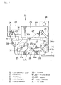
- the IC contact unit 22 is constructed as shown in FIGS. 2, 3 and 4.
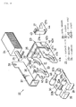
- this IC contact unit 22 includes a bracket 23 as a unit main body, a solenoid 24 as an actuator fixed to the bracket 23, an L-shaped arm 27 rotated and operated by a pin 26 attached to a plunger 25 of the solenoid 24, and a slider 30 as a movable support which is provided with, on its lower surface, an IC contact point 28 (see FIGS. 2 and 3) capable of coming in contact with a terminal of the IC card A, and in which a pawl member 29 is integrally or monolithically formed on the lower surface at the tip end side (left side of the drawing) in the card transfer direction.
- the bracket 23 includes a pair of side plates 32 and 33 for forming a slider arrangement space 31, a coupling plate 34 for mutually coupling both the side plates 32 and 33, a spring retainer 35 integrally and curvedly formed obliquely toward the front from the upper portion of the coupling plate 34, and a solenoid attachment plate 37 integrally provided to the one side plate 33 through a spacer 36.
- An attachment hole 38 used for attaching the IC contact unit 22 to the card reader main body 12 is formed in the attachment plate 37, and a hole portion 40 for disposing a support shaft 39 (see FIGS. 2 and 3) for support of the arm 27 is formed in a front end portion of the one side plate 33.
- guide holes 41 and 42 of the same shape are bored and formed at the opposite positions of the respective side plates 32 and 33.
- the front side guide hole 41 (left guide hole of FIG. 4) is formed to include a horizontal portion 41a, a slant portion 41b, and a vertical portion 41c
- the rear side guide hole 42 (right guide hole of FIG. 4) is formed to include a horizontal portion 42a and a slant portion 42b.
- the L-shaped arm 27 is an arm for depressing the slider 30, in which a vertical portion 27a and a horizontal portion 27b are integrally formed to be substantially L-shaped.
- a concave groove 43 (concave portion) loosely fitted to the pin 26 at the side of the plunger 25 is formed at the end portion of the vertical portion 27a, and a hole portion 44 in which the support shaft 39 is fitted, is formed at a corner portion of the vertical portion 27a and the horizontal portion 27b.
- shafts 45 and 46 are attached to a base portion 30a of the slider 30 in parallel with each other through a plurality of receiving portions 30b.
- the front and rear shafts 45 and 46 correspond to the guide holes 41 and 42 at the side of the bracket 23, and both end portions of the shafts 45 and 46 protruding outward from the receiving portions 30b become guide members movably inserted in the guide holes 41 and 42.
- FIG. 4 the respective components shown in the exploded perspective view are assembled as shown in FIGS. 2 and 3 and are arranged at a predetermined portion of the IC card reader 11.
- FIGS. 2 and 3 show a state at an ordinary time (normal time).
- the front and rear shafts 45 and 46 at the side of the slider 30 are movably inserted in the corresponding guide holes 41 and 42, and a coil spring 47 (return spring) as urging means for retreating the pawl member 29 upward from the card transfer line 13 at the ordinary time is stretched between the center of the front side shaft 45 in the longitudinal direction and the spring retainer 35.
- a coil spring 47 return spring
- the solenoid 24 moves the slider 30 downward at the time of attraction of the plunger 25 through the L-shaped arm 27, and projects the pawl portion 29 of the slider 30 to the card transfer line 13, and as shown in FIG. 1, when the end portion of the IC card A is engaged with the pawl portion 29, the slider 30 is moved by effectively using the transfer force of the IC card A.
- the pawl member 29 does not fall to the card transfer line 13, and it does not have an influence on the transfer of the IC card A.
- the magnetic head 21 executes reading of magnetic information such as customer data from the magnetic recording medium of the IC card A.
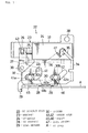
- the IC contact unit 22 is changed from the state shown in FIGS. 2 and 3 to the state shown in FIGS. 5 and 6.
- the slider 30 urged by the coil spring 47 is swung downward against the urging force with the rear side shaft 46 positioned at the upper end of the slant portion 42b of the guide hole 42 as a swing supporting point, and the pawl member 29 is projected to the card transfer line 13.
- the front side shaft 45 is displaced downward from the upper end of the vertical portion 41c of the guide hole 41 to the slant portion 41b as shown in FIGS. 5 and 6.
- the front side shaft 45 at the side of the slider 30 is moved from the slant portion 41b of the guide hole 41 to the horizontal portion 41a, and the rear side shaft 46 is also moved from the slant portion 42b of the guide hole 42 to the horizontal portion 42a, so that the IC contact point 28 of the lower surface of the slider 30 accurately comes in contact with the terminal provided in the IC card A.
- the IC contact unit 22 executes the read/write processing of variable data such as transaction data to the IC chip of the IC card A.
- the IC contact unit 22 of the embodiment is the IC contact unit including the movable support (see the slider 30) provided with the IC contact point 28 capable of coming in contact with the terminal of the IC card A and is constructed such that the guide portion (see the guide holes 41 and 42) for guiding the movable support (see the slider 30) swingably and movably in the front-back direction is provided in the unit main body (see the bracket 23), the guide member (see the shafts 45 and 46) to be inserted in the guide portion (see the guide holes 41 and 42) is provided at the movable support (see the slider 30), the pawl portion 29 to be engaged with the end portion of the IC card is formed at the movable support, the pawl portion 29 is projected to the card transfer surface (see the card transfer line 13) by the actuator (see the solenoid 24), and the movable support (see the slider 30) is moved by the transfer force of the IC card A.
- the pawl member 29 is projected to the card transfer surface (see the card transfer line 13) by the actuator (see the solenoid 24) through the movable support (see the slider 30), and when the end portion of the IC card A transferred on the card transfer surface (see the card transfer line 13) comes in contact with the pawl member 29, the movable support (see the slider 30) is moved by the card transfer force.
- the actuator may be a small one having a driving force of such a degree that the pawl member 29 is projected to the card transfer surface (see the card transfer line 13), so that the actuator (see the solenoid 24) can be miniaturized, and the whole apparatus can be made compact and consumed electric power can be reduced.
- positioning of the IC contact point 28 of the IC card A is carried out through the relation between the pawl member 29 and the guide portion (see the guide holes 41 and 42), high positioning accuracy can be ensured.
- the urging means for retreating the pawl member 29 from the card transfer surface (see the card transfer line 13) at the ordinary time (see FIGS. 2 and 3) is provided, and the pawl member 29 is projected to the card transfer surface (see the card transfer line 13) through the movable support (see the slider 30) at the time of driving of the actuator (see the solenoid 24).
- the projection timing of the pawl member 29 by the actuator can be freely and arbitrarily set.
- the IC card reader 11 of the embodiment includes the IC contact unit 22 of the above structure, the movable support (see the slider 30) can be driven by the small actuator (see the solenoid 24), and the degree of freedom in arrangement layout of the IC contact unit 22 in the IC card reader 11 is improved.
- the four guide holes 41, 41, 42, 42 in total are formed in the bracket 23 as the unit, and when both the end portions of the two shafts 45 and 46 at the side of the slider 30 are movably inserted in the corresponding portions of the guide holes 41 and 42, the stable movement of the slider 30 can be ensured.
- the movable support of the present invention corresponds to the slider 30 of the embodiment, and similarly in the following, the unit main body corresponds to the bracket 23, the guide portion at the side of the unit main body corresponds to the guide holes 41 and 42 at the side of the bracket 23, the guide member at the side of the movable support corresponds to the shafts 45 and 46 at the side of the slider 30, the actuator corresponds to the solenoid 24, the card transfer surface corresponds to the card transfer line 13, and the urging means corresponds to the coil spring 47 (return spring).
- the present invention is not limited only to the foregoing structure of the embodiment.
- the transfer force of the IC card is effectively used, there are effects that the actuator such as a solenoid can be made small, the whole apparatus can be made compact, and the consumed electric power can be reduced.
Landscapes
- Physics & Mathematics (AREA)
- General Physics & Mathematics (AREA)
- Engineering & Computer Science (AREA)
- Theoretical Computer Science (AREA)
- Credit Cards Or The Like (AREA)
- Conveying Record Carriers (AREA)
- General Electrical Machinery Utilizing Piezoelectricity, Electrostriction Or Magnetostriction (AREA)
- Coupling Device And Connection With Printed Circuit (AREA)
Abstract
Description
Claims (3)
- An IC contact unit comprising a movable support provided with an IC contact point capable of coming in contact with a terminal of an IC card, the IC contact unit comprising:wherein the pawl portion is projected to a card transfer surface by an actuator, and the movable support is moved by transfer force of the IC card.a guide portion, provided in a unit main body, for guiding the movable support;a guide member, provided at the movable support, to be inserted in the guide portion; anda pawl portion, formed at the movable support, to be engaged with an end portion of the IC card,
- An IC contact unit according to claim 1, further comprising urging means for retreating the pawl member from the card transfer surface at an ordinary time, wherein the pawl member is projected to the card transfer surface through the movable support at a driving time of the actuator.
- An IC card reader comprising an IC contact unit according to claim 1 or 2.
Applications Claiming Priority (2)
| Application Number | Priority Date | Filing Date | Title |
|---|---|---|---|
| JP2000305971 | 2000-10-05 | ||
| JP2000305971A JP3683489B2 (en) | 2000-10-05 | 2000-10-05 | IC contact unit and IC card reader |
Publications (3)
| Publication Number | Publication Date |
|---|---|
| EP1195709A2 true EP1195709A2 (en) | 2002-04-10 |
| EP1195709A3 EP1195709A3 (en) | 2002-10-02 |
| EP1195709B1 EP1195709B1 (en) | 2010-03-03 |
Family
ID=18786735
Family Applications (1)
| Application Number | Title | Priority Date | Filing Date |
|---|---|---|---|
| EP01308230A Expired - Lifetime EP1195709B1 (en) | 2000-10-05 | 2001-09-27 | IC contact unit and IC card reader |
Country Status (5)
| Country | Link |
|---|---|
| US (1) | US6779723B2 (en) |
| EP (1) | EP1195709B1 (en) |
| JP (1) | JP3683489B2 (en) |
| AT (1) | ATE459931T1 (en) |
| DE (1) | DE60141441D1 (en) |
Families Citing this family (2)
| Publication number | Priority date | Publication date | Assignee | Title |
|---|---|---|---|---|
| GB2391989B (en) * | 2001-04-12 | 2004-12-01 | Sankyo Seiki Seisakusho Kk | Card forcible ejection mechanism |
| CN107111731B (en) * | 2015-04-10 | 2019-11-29 | 日立欧姆龙金融系统有限公司 | IC contact unit, IC card processing device, and automatic transaction device |
Family Cites Families (12)
| Publication number | Priority date | Publication date | Assignee | Title |
|---|---|---|---|---|
| US3631535A (en) * | 1968-07-26 | 1971-12-28 | Credit Systems Inc | Credit card decoder |
| US4724310A (en) * | 1984-07-02 | 1988-02-09 | Tokyo Tatsuno Co., Ltd. | Device for inserting and holding an IC card as an external memory during reading and writing operations |
| FR2594988B1 (en) * | 1986-02-21 | 1989-11-24 | Radiotechnique Ind & Comm | APPARATUS FOR ESTABLISHING DATA TRANSFERS WITH A PORTABLE ELECTRONIC CARD |
| US4904852A (en) * | 1986-12-12 | 1990-02-27 | Omron Tateisi Electronics Co. | IC card reader |
| US4839509A (en) * | 1987-06-19 | 1989-06-13 | Diesel Kiki Co., Ltd. | Connector device for connecting IC card to reading and/or writing apparatus |
| ATE182999T1 (en) * | 1988-10-14 | 1999-08-15 | Omron Tateisi Electronics Co | CARD READER WITH LOCKING |
| AT394462B (en) * | 1990-06-01 | 1992-04-10 | Philips Nv | SCANNER DEVICE FOR A CHIP CARD |
| JP3209040B2 (en) * | 1995-05-31 | 2001-09-17 | 松下電器産業株式会社 | IC card device |
| DE69635742T2 (en) * | 1995-11-17 | 2006-09-14 | Kabushiki Kaisha Toshiba, Kawasaki | Device for card processing |
| US5917177A (en) | 1995-12-13 | 1999-06-29 | Sankyo Seiki Mfg. Co., Ltd. | IC card reader |
| US6149064A (en) * | 1998-03-06 | 2000-11-21 | Kabushiki Kaisha Sankyo Seiki Seisakusho | IC card reader |
| JP3362691B2 (en) * | 1999-03-08 | 2003-01-07 | 松下電器産業株式会社 | IC card reader |
-
2000
- 2000-10-05 JP JP2000305971A patent/JP3683489B2/en not_active Expired - Fee Related
-
2001
- 2001-09-27 AT AT01308230T patent/ATE459931T1/en not_active IP Right Cessation
- 2001-09-27 DE DE60141441T patent/DE60141441D1/en not_active Expired - Lifetime
- 2001-09-27 EP EP01308230A patent/EP1195709B1/en not_active Expired - Lifetime
- 2001-10-01 US US09/966,592 patent/US6779723B2/en not_active Expired - Lifetime
Also Published As
| Publication number | Publication date |
|---|---|
| US20020040931A1 (en) | 2002-04-11 |
| ATE459931T1 (en) | 2010-03-15 |
| DE60141441D1 (en) | 2010-04-15 |
| EP1195709B1 (en) | 2010-03-03 |
| JP2002117375A (en) | 2002-04-19 |
| US6779723B2 (en) | 2004-08-24 |
| EP1195709A3 (en) | 2002-10-02 |
| JP3683489B2 (en) | 2005-08-17 |
Similar Documents
| Publication | Publication Date | Title |
|---|---|---|
| US6761569B2 (en) | Card connector device | |
| EP0895178A2 (en) | Card connector | |
| JP2005071667A (en) | Memory card connector | |
| EP1195709B1 (en) | IC contact unit and IC card reader | |
| EP1195747B1 (en) | Support structure of a magnetic head and magnetic card reader | |
| US4232349A (en) | Mode switching mechanism for a cassette tape recorder | |
| JPH11509020A (en) | Card reader for two types of data cards | |
| US4437132A (en) | Flexible magnetic disk device | |
| EP0293888B1 (en) | Ic card reader | |
| JPH0743759B2 (en) | Punch movable magnetic card reader | |
| US6457648B1 (en) | Dual-interface card reading device | |
| CN221993974U (en) | IC card holder and POS machine | |
| JP2839946B2 (en) | Interlock mechanism of IC card reader / writer | |
| US4455951A (en) | Embroidery lace machine driven by electric signals | |
| JPH0720779Y2 (en) | Card reader / writer | |
| JP2002074282A (en) | Multi-card reader | |
| JPH11250195A (en) | Smart card reader | |
| JPH0521168Y2 (en) | ||
| JP3567201B2 (en) | IC card processing device | |
| JP2839947B2 (en) | Eject mechanism for IC card reader / writer | |
| KR100341046B1 (en) | Card processing apparatus | |
| WO2010084814A1 (en) | Connector for card | |
| JPH11191458A (en) | Memory card connector | |
| US20060158965A1 (en) | Gear train module and electronic device utilizing the same | |
| JPH0610825B2 (en) | Magnetic card reader / writer with punch unit |
Legal Events
| Date | Code | Title | Description |
|---|---|---|---|
| PUAI | Public reference made under article 153(3) epc to a published international application that has entered the european phase |
Free format text: ORIGINAL CODE: 0009012 |
|
| AK | Designated contracting states |
Kind code of ref document: A2 Designated state(s): AT BE CH CY DE DK ES FI FR GB GR IE IT LI LU MC NL PT SE TR |
|
| AX | Request for extension of the european patent |
Free format text: AL;LT;LV;MK;RO;SI |
|
| PUAL | Search report despatched |
Free format text: ORIGINAL CODE: 0009013 |
|
| AK | Designated contracting states |
Kind code of ref document: A3 Designated state(s): AT BE CH CY DE DK ES FI FR GB GR IE IT LI LU MC NL PT SE TR |
|
| AX | Request for extension of the european patent |
Free format text: AL;LT;LV;MK;RO;SI |
|
| 17P | Request for examination filed |
Effective date: 20021028 |
|
| AKX | Designation fees paid |
Designated state(s): AT BE CH CY DE DK ES FI FR GB GR IE IT LI LU MC NL PT SE TR |
|
| RAP1 | Party data changed (applicant data changed or rights of an application transferred) |
Owner name: HITACHI-OMRON TERMINAL SOLUTIONS, CORP. |
|
| 17Q | First examination report despatched |
Effective date: 20070919 |
|
| GRAP | Despatch of communication of intention to grant a patent |
Free format text: ORIGINAL CODE: EPIDOSNIGR1 |
|
| GRAS | Grant fee paid |
Free format text: ORIGINAL CODE: EPIDOSNIGR3 |
|
| GRAA | (expected) grant |
Free format text: ORIGINAL CODE: 0009210 |
|
| AK | Designated contracting states |
Kind code of ref document: B1 Designated state(s): AT BE CH CY DE DK ES FI FR GB GR IE IT LI LU MC NL PT SE TR |
|
| REG | Reference to a national code |
Ref country code: GB Ref legal event code: FG4D |
|
| REG | Reference to a national code |
Ref country code: CH Ref legal event code: EP |
|
| REG | Reference to a national code |
Ref country code: IE Ref legal event code: FG4D |
|
| REF | Corresponds to: |
Ref document number: 60141441 Country of ref document: DE Date of ref document: 20100415 Kind code of ref document: P |
|
| REG | Reference to a national code |
Ref country code: NL Ref legal event code: VDEP Effective date: 20100303 |
|
| PG25 | Lapsed in a contracting state [announced via postgrant information from national office to epo] |
Ref country code: FI Free format text: LAPSE BECAUSE OF FAILURE TO SUBMIT A TRANSLATION OF THE DESCRIPTION OR TO PAY THE FEE WITHIN THE PRESCRIBED TIME-LIMIT Effective date: 20100303 Ref country code: AT Free format text: LAPSE BECAUSE OF FAILURE TO SUBMIT A TRANSLATION OF THE DESCRIPTION OR TO PAY THE FEE WITHIN THE PRESCRIBED TIME-LIMIT Effective date: 20100303 |
|
| PG25 | Lapsed in a contracting state [announced via postgrant information from national office to epo] |
Ref country code: SE Free format text: LAPSE BECAUSE OF FAILURE TO SUBMIT A TRANSLATION OF THE DESCRIPTION OR TO PAY THE FEE WITHIN THE PRESCRIBED TIME-LIMIT Effective date: 20100303 Ref country code: ES Free format text: LAPSE BECAUSE OF FAILURE TO SUBMIT A TRANSLATION OF THE DESCRIPTION OR TO PAY THE FEE WITHIN THE PRESCRIBED TIME-LIMIT Effective date: 20100614 Ref country code: GR Free format text: LAPSE BECAUSE OF FAILURE TO SUBMIT A TRANSLATION OF THE DESCRIPTION OR TO PAY THE FEE WITHIN THE PRESCRIBED TIME-LIMIT Effective date: 20100604 Ref country code: NL Free format text: LAPSE BECAUSE OF FAILURE TO SUBMIT A TRANSLATION OF THE DESCRIPTION OR TO PAY THE FEE WITHIN THE PRESCRIBED TIME-LIMIT Effective date: 20100303 Ref country code: CY Free format text: LAPSE BECAUSE OF FAILURE TO SUBMIT A TRANSLATION OF THE DESCRIPTION OR TO PAY THE FEE WITHIN THE PRESCRIBED TIME-LIMIT Effective date: 20100303 Ref country code: BE Free format text: LAPSE BECAUSE OF FAILURE TO SUBMIT A TRANSLATION OF THE DESCRIPTION OR TO PAY THE FEE WITHIN THE PRESCRIBED TIME-LIMIT Effective date: 20100303 |
|
| PLBE | No opposition filed within time limit |
Free format text: ORIGINAL CODE: 0009261 |
|
| STAA | Information on the status of an ep patent application or granted ep patent |
Free format text: STATUS: NO OPPOSITION FILED WITHIN TIME LIMIT |
|
| PG25 | Lapsed in a contracting state [announced via postgrant information from national office to epo] |
Ref country code: DK Free format text: LAPSE BECAUSE OF FAILURE TO SUBMIT A TRANSLATION OF THE DESCRIPTION OR TO PAY THE FEE WITHIN THE PRESCRIBED TIME-LIMIT Effective date: 20100303 Ref country code: PT Free format text: LAPSE BECAUSE OF FAILURE TO SUBMIT A TRANSLATION OF THE DESCRIPTION OR TO PAY THE FEE WITHIN THE PRESCRIBED TIME-LIMIT Effective date: 20100705 |
|
| 26N | No opposition filed |
Effective date: 20101206 |
|
| PG25 | Lapsed in a contracting state [announced via postgrant information from national office to epo] |
Ref country code: IT Free format text: LAPSE BECAUSE OF FAILURE TO SUBMIT A TRANSLATION OF THE DESCRIPTION OR TO PAY THE FEE WITHIN THE PRESCRIBED TIME-LIMIT Effective date: 20100303 |
|
| PG25 | Lapsed in a contracting state [announced via postgrant information from national office to epo] |
Ref country code: MC Free format text: LAPSE BECAUSE OF NON-PAYMENT OF DUE FEES Effective date: 20100930 |
|
| REG | Reference to a national code |
Ref country code: CH Ref legal event code: PL |
|
| PG25 | Lapsed in a contracting state [announced via postgrant information from national office to epo] |
Ref country code: LI Free format text: LAPSE BECAUSE OF NON-PAYMENT OF DUE FEES Effective date: 20100930 Ref country code: IE Free format text: LAPSE BECAUSE OF NON-PAYMENT OF DUE FEES Effective date: 20100927 Ref country code: CH Free format text: LAPSE BECAUSE OF NON-PAYMENT OF DUE FEES Effective date: 20100930 |
|
| PG25 | Lapsed in a contracting state [announced via postgrant information from national office to epo] |
Ref country code: LU Free format text: LAPSE BECAUSE OF NON-PAYMENT OF DUE FEES Effective date: 20100927 |
|
| PG25 | Lapsed in a contracting state [announced via postgrant information from national office to epo] |
Ref country code: TR Free format text: LAPSE BECAUSE OF FAILURE TO SUBMIT A TRANSLATION OF THE DESCRIPTION OR TO PAY THE FEE WITHIN THE PRESCRIBED TIME-LIMIT Effective date: 20100303 |
|
| REG | Reference to a national code |
Ref country code: FR Ref legal event code: PLFP Year of fee payment: 16 |
|
| PGFP | Annual fee paid to national office [announced via postgrant information from national office to epo] |
Ref country code: GB Payment date: 20160921 Year of fee payment: 16 Ref country code: DE Payment date: 20160920 Year of fee payment: 16 |
|
| PGFP | Annual fee paid to national office [announced via postgrant information from national office to epo] |
Ref country code: FR Payment date: 20160816 Year of fee payment: 16 |
|
| REG | Reference to a national code |
Ref country code: DE Ref legal event code: R119 Ref document number: 60141441 Country of ref document: DE |
|
| GBPC | Gb: european patent ceased through non-payment of renewal fee |
Effective date: 20170927 |
|
| REG | Reference to a national code |
Ref country code: FR Ref legal event code: ST Effective date: 20180531 |
|
| PG25 | Lapsed in a contracting state [announced via postgrant information from national office to epo] |
Ref country code: DE Free format text: LAPSE BECAUSE OF NON-PAYMENT OF DUE FEES Effective date: 20180404 Ref country code: GB Free format text: LAPSE BECAUSE OF NON-PAYMENT OF DUE FEES Effective date: 20170927 |
|
| PG25 | Lapsed in a contracting state [announced via postgrant information from national office to epo] |
Ref country code: FR Free format text: LAPSE BECAUSE OF NON-PAYMENT OF DUE FEES Effective date: 20171002 |