EP1195603A2 - Electrophoretic device and method of manufacturing it - Google Patents
Electrophoretic device and method of manufacturing it Download PDFInfo
- Publication number
- EP1195603A2 EP1195603A2 EP01308454A EP01308454A EP1195603A2 EP 1195603 A2 EP1195603 A2 EP 1195603A2 EP 01308454 A EP01308454 A EP 01308454A EP 01308454 A EP01308454 A EP 01308454A EP 1195603 A2 EP1195603 A2 EP 1195603A2
- Authority
- EP
- European Patent Office
- Prior art keywords
- electrophoretic
- electrodes
- ferroelectric substance
- electrophoretic device
- manufacturing
- Prior art date
- Legal status (The legal status is an assumption and is not a legal conclusion. Google has not performed a legal analysis and makes no representation as to the accuracy of the status listed.)
- Granted
Links
Images





Classifications
-
- G—PHYSICS
- G02—OPTICS
- G02F—OPTICAL DEVICES OR ARRANGEMENTS FOR THE CONTROL OF LIGHT BY MODIFICATION OF THE OPTICAL PROPERTIES OF THE MEDIA OF THE ELEMENTS INVOLVED THEREIN; NON-LINEAR OPTICS; FREQUENCY-CHANGING OF LIGHT; OPTICAL LOGIC ELEMENTS; OPTICAL ANALOGUE/DIGITAL CONVERTERS
- G02F1/00—Devices or arrangements for the control of the intensity, colour, phase, polarisation or direction of light arriving from an independent light source, e.g. switching, gating or modulating; Non-linear optics
- G02F1/01—Devices or arrangements for the control of the intensity, colour, phase, polarisation or direction of light arriving from an independent light source, e.g. switching, gating or modulating; Non-linear optics for the control of the intensity, phase, polarisation or colour
- G02F1/165—Devices or arrangements for the control of the intensity, colour, phase, polarisation or direction of light arriving from an independent light source, e.g. switching, gating or modulating; Non-linear optics for the control of the intensity, phase, polarisation or colour based on translational movement of particles in a fluid under the influence of an applied field
- G02F1/166—Devices or arrangements for the control of the intensity, colour, phase, polarisation or direction of light arriving from an independent light source, e.g. switching, gating or modulating; Non-linear optics for the control of the intensity, phase, polarisation or colour based on translational movement of particles in a fluid under the influence of an applied field characterised by the electro-optical or magneto-optical effect
- G02F1/167—Devices or arrangements for the control of the intensity, colour, phase, polarisation or direction of light arriving from an independent light source, e.g. switching, gating or modulating; Non-linear optics for the control of the intensity, phase, polarisation or colour based on translational movement of particles in a fluid under the influence of an applied field characterised by the electro-optical or magneto-optical effect by electrophoresis
Definitions
- This invention relates to electrophoretic devices such as electrophoretic displays which contain electrophoretic dispersion liquids containing electrophoretic particles dispersed in a liquid phase dispersion medium, wherein the electrophoretic dispersion liquid is arranged between electrodes that are arranged opposite to each other and are electrified to attract the particles in different directions respectively.
- this invention also relates to methods of manufacturing the electrophoretic devices.
- FIG. 8A shows a structure of the disclosed electrophoretic display, wherein an electrode 3 is arranged on a substrate 1 while a transparent electrode 4 is arranged below a transparent substrate 2. The space between these electrodes 3 and 4 is filled with electrophoretic dispersion liquid 50. In addition, spacers 7 are provided to prevent bleeding of the electrophoretic dispersion liquid 50 from the electrophoretic display.
- FIG. 8A shows only a selected section ofthe electrophoretic display for one pixel.
- the electrophoretic dispersion liquid 50 contain electrophoretic particles 5 that are dispersed in liquid phase dispersion medium 6. Different colors are applied to the electrophoretic particles 5 and the liquid phase dispersion medium 6 respectively.
- the electrophoretic display is connected to two voltage sources 9a and 9b by way of a switch 8.
- the voltage sources 9a and 9b apply voltages between the electrodes 3 and 4 with opposite polarities. That is, the electrode 4 is directly connected with the negative terminal of the voltage source 9a and the positive terminal of the voltage source 9b, whereas the electrode 3 is connected with either the positive terminal of the voltage source 9a or the negative terminal of the voltage source 9b by way of the switch 8.
- the aforementioned connections allow alternation of the polarity of the voltage by switching the switch 8.
- the electrophoretic dispersion liquid 50 is adequately subjected to polarization to enable the desired images to be displayed by the electrophoretic display.
- the electrophoretic particles 5 move towards the transparent electrode 4, which is observed by a human observer. In this state, the human observer views the color of the electrophoretic particles 5 with his/her eyes.
- the electrophoretic particles 5 move towards the electrode 3, which is arranged opposite to the transparent electrode 4 being observed by the human observer. In this state, the human observer views the color of the liquid phase dispersion medium 6.
- the aforementioned structure of the electrophoretic display shown in FIG. 8A allows the human observer to view two colors, which can be displayed on the screen by switching the direction of the voltage applied between the electrodes 3 and 4. Therefore, the overall configuration of the electrophoretic display can be realized by providing the aforementioned structure for each pixel on the screen.
- Japanese Examined Patent Publication No. Sho 50-15115 teaches a technique for retaining the display contents. Specifically, it teaches the use of a specific dispersion medium that is solidified at normal temperatures and that can be softened by heat or a solvent. The aforementioned technique requires complicated steps in writing images, such as heating steps.
- Japanese Unexamined Utility-Model Publication No. Hei 2-51325 discloses another technique that uses liquid crystal for the dispersion medium.
- this technique is disadvantageous because only a limited range of materials can be used for the dispersion medium.
- U.S. Patent No. 5,961,804 discloses an electrophoretic display having the specific structure in which charged elements having the polarity opposite to that of the particles are restrained inside of microcapsules containing dispersion liquids.
- it is very difficult to carry out the charge restraining method, which complicates the manufacturing processes.
- it is disadvantageous because only a limited range of materials can be used for the microcapsules.
- Japanese Unexamined Patent Publication No. Hei 3-213827 discloses a technique for refreshing displayed images by periodically applying a drive voltage to the electrophoretic display. However, it is complicated in control and is disadvantageous because of the large consumption of electricity. For this reason, it is very difficult to apply the aforementioned technique to the electronic paper.
- This invention provides unique and easy-to-manufacture structures for electrophoretic devices such as electrophoretic displays, in which an electrophoretic dispersion liquid containing electrophoretic particles dispersed in the liquid phase dispersion medium is contained in a space between electrodes, at least one of which is composed of transparent materials.
- This invention is characterized by arranging ferroelectric substance layers between the electrodes, which are arranged opposite to each other. The provision of the ferroelectric substance layers, which are arranged between the electrodes, allows the polarized state of the electrophoretic dispersion liquid to be maintained for a long time. Thus, it is possible to improve the image retaining capability of the electrophoretic device.
- the ferroelectric substance layers are connected in series within the space formed between the electrodes. Therefore, it is possible to enlarge the overall effective area of the ferroelectric substance layers, which makes it effectively maintain the polarized state of the electrophoretic dispersion liquid. In addition, it is possible to simplify the structure of the electrophoretic device, which can be manufactured with ease.
- ferroelectric substance layers are arranged in parallel between the electrodes. In this case, it is possible to reduce the drive voltage applied between the electrodes because of the parallel arrangement of the ferroelectric substance layers between the electrodes.
- a switch enabling repetitive and reversible switching between the electrophoretic dispersion liquid and the ferroelectric substance layers to be electrically connected in series or in parallel.
- the ferroelectric substance layers and the electrophoretic dispersion liquid are electrically connected in parallel, it is possible to reduce the drive voltage, which is applied between the electrodes.
- the ferroelectric substance layers and the electrophoretic dispersion liquid are electrically connected in series, which makes it possible to effectively retain the polarized state of the electrophoretic dispersion liquid.
- ferroelectric substance layers are composed of organic polymer ferroelectric substances, it is possible to form the ferroelectric substance layers by prescribed printing and painting methods using an organic solvent solution, for example. This provides an easy way to manufacture the electrophoretic device.
- At least one of the electrodes is partitioned into a plurality of sections in relation to a plurality of pixels on the screen.
- the ferroelectric substance layers can be also partitioned into a plurality of sections in relation to the pixels respectively. These sections of the ferroelectric substance layers are not necessarily provided for all of the pixels on the screen. Hence, it is possible to provide them for desired locations of the pixels respectively. This enables different contents to be displayed with respect to the pixels respectively. Therefore, it is possible to display the desired images on the screen.
- the ferroelectric substance layer is formed by a prescribed method using an organic solvent solution for use in organic polymer ferroelectric substances and the like.
- the prescribed method it is possible to employ the inkjet printing method, screen process printing method, spin-coating method, roll-coating method, etc. These methods do not require the special equipment such as a vacuum chamber Hence, it is possible to manufacture the electrophoretic device at a relatively low cost.
- a first manufacturing method is to form the layer of the electrophoretic dispersion liquid after formation of the ferroelectric substance layers in accordance with a prescribed method.
- a parallel arrangement of the ferroelectric substance layers which create spaces for arranging microcapsules between the electrodes.
- a second manufacturing method is to form the ferroelectric substance layers after the formation of the layer of the electrophoretic dispersion liquid in accordance with a prescribed method.
- a serial arrangement of the ferroelectric substance layers within the space formed between the electrodes.
- FIG. 2 is a sectional view showing a structure of an electrophoretic device (namely, an electrophoretic display) in accordance with a first embodiment of the invention.
- the electrophoretic device is composed of a number of microcapsules 51 each encapsulating electrophoretic particles 5 and a liquid phase dispersion medium (namely, dispersion liquid) 6 as shown in FIG. 3.
- the microcapsules 51 are introduced into a binder and are colored in correspondence with the pixels.
- the dispersion liquid 6 also contain ions whose polarity is opposite to that of the electrophoretic particles 5.
- the electrophoretic particles 5 move towards on one electrode while the ions having the opposite polarity move towards another electrode.
- the dispersion liquid 6 is subjected to a polarization that allows the coexistence of electric dipoles.
- the present embodiment provides a ferroelectric substance layer 10, whereby the polarized state is maintained by using the ferroelectric substances' residual polarization characteristics.
- the display is maintained for a time even though the voltage application is terminated. Therefore, it is possible to provide the electronic paper whose display contents can be adequately updated or rewritten.
- the electronic paper is made using the conventional electrophoretic display, it is difficult to maintain display contents (e.g. , images) on the screen for a long time after the termination of the application of a voltage.
- FIG. 2 shows the series connection of ferroelectric substances, which are connected in series to form the ferroelectric substance layer 10 that is arranged between the electrode 3 and the transparent electrode 4.
- FIG. 2 shows an example of the structure in which the ferroelectric substance layer 10 corresponding to the series connection of ferroelectric substances is arranged below and in contact with the transparent electrode 4.
- the electrode 3 is divided into a number of pieces in correspondence with the pixels.
- the transparent electrode 4 is partitioned into a number of sections, which form the pixels on the screen.
- FIG. 1A Due to the aforementioned structure, it is possible to establish an in-series electric connection between the electrophoretic dispersion liquid 50 and the ferroelectric substance layer 10, which is shown in FIG. 1A.
- the electrophoretic dispersion liquid 50 has a resistance R EP and a capacitance C EP while the ferroelectric substance layer has a capacitance C FE .
- the structure of the electrophoretic device of FIG. 1A can be described by the equivalent circuit shown in FIG. 1B in which a parallel circuit consisting of a resistor R EP and a capacitor C EP is connected in series with a capacitor C FE .
- the voltage source 9a or 9b provides the application of a voltage V in , by which the electrophoretic dispersion liquid 50 bears partial voltage V EP while the ferroelectric substance layer 10 bears partial voltage V FE .
- V in V EP +V FE
- VDE/TrFE vinylidene/trifluoroethylene
- C FE :C EP 2:1, it is possible to determine a relationship of 'V in ⁇ 24V'.
- FIG. 4 shows another structure of the electrophoretic device, which provides a parallel connection of ferroelectric substances, which are connected in parallel to form a ferroelectric substance layer 10 that is arranged between the electrode 3 and the transparent electrode 4.
- the electrode 3 is partitioned into a number of sections to provide a number of pixels on the screen.
- the ferroclectrio substance layer 10 is also partitioned into a number of sections in correspondence with the pixels.
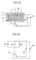
- FIG. 5A shows an internal configuration of the electrophoretic device that provides a parallel connection of ferroelectric substance layers 10, wherein the ferroelectric substance layers 10 are arranged vertically between the electrode 3 and the transparent electrode 4.
- the electrophoretic device of FIG. 5A can be described by the equivalent circuit of FIG. 5B, wherein all of the capacitor C EP , resistor R EP and capacitor C FE are connected in parallel.
- the voltage source 9a or 9b applies a voltage V in by which the electrophoretic dispersion liquid 50 bears partial voltage V EP while the ferroelectric substance layer 10 bears partial voltage V FE .
- the parallel circuit shown in FIG. 5B establishes the following relationship.
- the electrophoretic device can be partially modified to carry out switching between the serial connection and parallel connection for the electrophoretic dispersion liquid 50 and the ferroelectric substance layer 10.
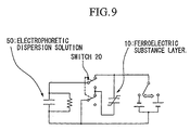
- FIG. 9 shows an equivalent circuit for the modified electrophoretic device, wherein a parallel circuit consisting of a resistance and a capacitance is the electrical equivalent of the electrophoretic dispersion liquid 50, while the variable capacitance is the electrical equivalent of the ferroelectric substance layer 10.
- a switch 20 is connected between the parallel circuit and the variable capacitance to provide the repetitive or reversible switching between a serial connection and a parallel connection.
- the electrophoretic dispersion liquid 50 and the ferroelectric substance layer 10 are electrically connected in parallel.
- the drive voltage can be reduced in the drive mode.
- the electrophoretic dispersion liquid 50 and the ferroelectric substance layer 10 are electrically connected in series. In the non-drive mode, it is possible to effectively maintain the polarized state of the electrophoretic dispersion liquid.
- the material for use in the ferroelectric substance connected in series or in parallel is selected from among inorganic dielectric materials, organic polymer dielectric materials and their complex materials. Specifically, it is necessary to select materials from among the aforementioned materials that solidify at normal temperatures and that have a sufficiently high Curie point.
- inorganic dielectric materials it is possible to use lead zirconate titanate (PZT), barium titanate (BaTiO 3 ), lead titanate, and the like.
- organic polymer dielectric materials it is possible to use polyvinylidene fluoride (PVDF), copolymers ofvinylidene (VDF) / trifluoethylene (TrFE), copolymers of vinylidene cyanide (VDCN) / vinyl acetate (VAc), and the like. It is also possible to use a complex material that is made by dispersing micro-powders of the aforementioned inorganic dielectric materials into a polymer matrix made of PVDF or rubber.
- PVDF polyvinylidene fluoride
- VDF copolymers ofvinylidene
- TrFE trifluoethylene
- VDCN vinylidene cyanide
- VAc vinyl acetate
- the electrophoretic device shown in FIG. 2 is constituted so as to provide ferroelectric substance layers in correspondence with the pixels. It is not always required to provide a ferroelectric substance layer for each pixel. Hence, it is possible to provide the ferroelectric substance layers for only selected pixels that have a reduced image maintaining capability. To realize functions of an electronic paper, it is necessary to write display data to electrodes, which are arranged in proximity to the end portions of the electronic paper. In this case, it can be assumed that pixels, which are far from the electrodes, may have a reduced image maintaining capability compared with other pixels. Therefore, the ferroelectric substance layers can be provided for these pixels.
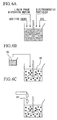
- FIG. 6A the liquid phase dispersion medium, electrophoretic particles, dye, and additive agent are put into a container and are stirred. Stirring provides the electrophoretic dispersion liquid 50.
- FIG. 6B the electrophoretic dispersion liquid 50 is put into a container in which it is stirred together with water and capsule wall materials 60. The stirred liquid is subjected to emulsification to form the capsule walls.
- FIG. 6C an emulsifier 61 is introduced into the container to harden the capsule walls.
- liquid phase dispersion medium it is possible to use water; alcohol solvents such as methanol, ethanol, isopropanol, butanol, octanol, and methyl cellusolve; esters such as ethyl acetate, and butyl acetate; ketones such as acetone, methyl ethyl ketone, methyl isobutyl ketone; aliphatic hydrocarbons such as pentane, hexane, and octane; alicyclic hydrocarbons such as cyclohexane, and methyl cyclohexane; aromatic hydrocarbons of the benzene family having long-chain alkyl groups such as benzene, toluene, xylene, hexylbenzene, heptylbenzene, octylbenzene, nonylbenzene, decylbenzene, undecylbenzene, dodecy
- Tn addition it is possible to use carboxylic acid or other oil materials.
- any of the oil materials can be independently used for the liquid phase dispersion medium.
- the electrophoretic particles can be organic or inorganic particles (or polymers or colloids) that tend to move due to potential differences in the dispersion medium under the influence of electrophoretic effects.
- the electrophoretic particles can be colored by using one pigment, or two or more pigments that have specific colors such as black, white, yellow, red, blue, and green.
- black pigments it is possible to use aniline black, and carbon black.
- white pigments it is possible to use titanium dioxide, zinc white, and antimony trioxide.
- azo pigments it is possible to use monoazo, disazo, and polyazo.
- As yellow pigments it is possible to use iso-indolynone, yellow lead, yellow iron oxide, cadmium yellow, titan yellow, and antimony.
- red pigments it is possible to use quinacrine red, and chrome bar million.
- blue pigments it is possible to use phthalocyanine blue, induslene blue, anthraquinone dye, ion blue, ultramarine blue, and cobalt blue.
- green pigments it is possible to use phthalocyanine green.
- additive materials or agents it is possible to add other materials or agents to the aforementioned pigments as necessary.
- additive materials or agents it is possible to use electrolytic elements, surface active agents, metal soap, resin, rubber, oil, varnish, charged control agents containing particles such as compounds, dispersing agents (such as titanium coupling agents, aluminum coupling agents, and silane coupling agents), lubricants, and stabilizing agents.
- the dispersion liquid that is composed as described above is subjected to sufficient admixture by an appropriate method, such as one using a ball mill, sand mill, and paint shaker. Then, the dispersion liquid is subjected to microencapsulating by an known microencapsulating method such as interfacial polymerization, an insolubilized reaction method, phase separation method, and interfacial precipitation.
- an appropriate method such as one using a ball mill, sand mill, and paint shaker.
- microencapsulating such as interfacial polymerization, an insolubilized reaction method, phase separation method, and interfacial precipitation.
- microcapsules 51 As the materials for use in formation of the microcapsules 51, it is preferable to use flexible materials such as compounds of Arabic rubber and gelatin, and urethane compounds. In order to demonstrate superior display properties, it is preferable that microcapsules 51 have an approximately uniform size. Microcapsules having an approximately uniform size can be produced by filtration or specific gravity difference separation. Normally, the size of the microcapsules ranges between 30 ⁇ m and 60 ⁇ m, for example.
- the microcapsules 51 are mixed together with the desired dielectric constant adjusting agent within the binder resin, so that a resin composition (e.g., emulsion or organic solvent solution) is produced.
- a resin composition e.g., emulsion or organic solvent solution
- the microcapsule layer is formed on the substrate by a known coating method such as the roll coater method, roll laminator method, screen process printing method, and spray method.
- the materials for use in the binder resin it is possible to use polyethylene, chlorinated polyethylene, copolymers of ethylene and vinyl acetate, copolymers of ethylene and ethyl acrylate, polypropylene, ABS resin, methyl methacrylate resins, vinyl chloride resins, copolymers of vinyl chloride and vinyl acetate, copolymers of vinyl chloride and vinylidene chloride, copolymers of vinyl chloride and acrylic ester, copolymers of vinyl chloride and methacrylic acid, copolymers of vinyl chloride and acrylonitrile, copolymers of ethylene, vinyl alcohol and vinyl chloride, copolymers of propylene and vinyl chloride, vinylidene chloride resin, vinyl acetate resin, polyvinyl alcohol, polyvinyl formal, thermoplastic resins such as cellulose resins, polyamidc resins, polyacetal, polycarbonate, polyethylene terephthalate, polybutylene terephtalate, polyphenylene
- dielectric constants of the electrophoretic solution and dispersed materials are set to approximately the same value with respect to the binder material.
- alcohols ketones, carboxylic acid, and the like to the binder resin composition, for example.
- the alcohols it is possible to use 1, 2-butanediol, 1, 4-butandiol, etc.
- a roll of transparent substrate material 71 on which the structure of the electrophoretic device is to be formed by the roll-to-roll method and inkjet manufacture method.
- the rolled transparent substrate material 71 it is possible to use a composition in which an ITO electrode film (where 'ITO' stands for 'Indium Tin Oxide') is formed on a heat-resistant film, for example. It is also possible to use a composition in which an ITO electrode film is formed on a PET substrate.
- the ITO electrode film is realized by the tin-doped indium oxide film.
- the electrode film by fluorine-doped tin oxide film (i.e., FTO film), antimony-doped zinc oxide film, indium-doped zinc oxide film, aluminum-doped zinc oxide film, and the like.
- FTO film fluorine-doped tin oxide film
- antimony-doped zinc oxide film indium-doped zinc oxide film
- aluminum-doped zinc oxide film and the like.
- the transparent substrate material 71 is output from a roller 70 and is subjected to painting with an organic polymer ferroelectric substance solution 73 by the inkjet printing method. That is, a nozzle 72 sprays the organic polymer ferroelectric substance solution 73 towards the ITO electrode film formed on the transparent substrate material 71.
- the organic polymer ferroelectric material it is necessary to use organic polymer ferroelectric substances having solvent solubility. For example, it is. possible to use a copolymer of VDF/TrFE.
- the organic polymer ferroelectric substance solution 73 sprayed on the ITO electrode film of the transparent substrate material 71 is subjected to annealing by hot air 74 to perform recrystallization.
- the temperature of the hot air 74 should be equal to the heat-resistant temperature of the heat-resistant film or PET, which is used for the rolled transparent substrate material 71, or less. That is, it is appropriate to set the temperature of the hot air 74 at 145°C or so.
- the conditions for film formation depend upon the dielectric constants of the dielectric substance layer, which are required for the electrophoretic device.
- the voltage applied to the dielectric substance layer and electrophoretic dispersion liquid increases or decreases in proportion to the inverse of the dielectric constant. Therefore, the film thickness should be determined in consideration of the dielectric constant. Preferably, the film thickness approximately ranges between 100 nm and 1 ⁇ m.
- microcapsule-dispersed liquid is produced by the foregoing steps shown in Figures 6A to 6C.
- the microcapsule-dispersed liquid is mixed with a water-soluble binder to produce the liquid 75, which is then coated to the layer of the 'annealed' organic polymer ferroelectric substance solution 73 formed on the ITO electrode film of the transparent substrate material 71 by means of a knife coater 76 and a roll 77.
- a water-soluble binder it is possible to use the silicone coating agent, for example.
- the layer of the 'coated' water-soluble binder on the transparent substrate material 71 is subjected to a drying operation by hot air 78.
- the temperature of the hot air 78 is set to 90°C approximately.
- the mixing ratio of binder in the liquid 75 and the coat thickness are determined in consideration of the thickness of the 'dried' microcapsule layer.
- the transparent substrate material 71 having the ITO electrode film, organic polymer dielectric substance layer, and microcapsule layer is laminated with a roll substrate material. 79 by means of rollers 80a and 80b. Finally, the 'laminated' substrate material is wound around a roller 81.
- the roll substrate material 79 has a laminated structure in which electrode patterns are formed on the plastic film made of PET or PI, for example.
- the coating process of the organic polymer ferroelectric substance solution 73 and the annealing process using hot air 74 are performed after the coating process of the liquid 75, in which the water-soluble binder is mixed with the microcapsule-dispersed liquid, and then the drying process using the hot air 78 is carried out.
- the ferroelectric substance layers are formed by the inkjet printing method.
- other known methods such as the screen process printing method, the offset printing method, spin-coating method, and roll-coating method, for example.
- electrophoretic devices such as electrophoretic displays without using special equipment such as vacuum chambers.
- the aforementioned electrophoretic devices can be driven by either the active method or passive method.
- the electrophoretic device of this invention is applicable to a variety of electronic devices having displays. Next, descriptions will be given with respect to examples of the electronic devices, each of which is able to use the electrophoretic device of this invention.
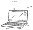
- FIG. 10 shows an external appearance of the personal computer 100, which basically comprises a main unit 102 providing a keyboard 103.
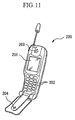
- FIG. 11 shows an external appearance ofthe cellular phone 200, which basically comprises numeric keys and function keys 202, an earpiece 203, and a mouthpiece 204.
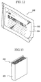
- FIG. 12 shows an external appearance of the electronic paper 300, which basically comprises a rewritable sheet 302 that has similar touch and flexibility of conventional papers.
- FIG. 13 shows an external appearance of an electronic notebook 400 in which a number of electronic papers 300 are bound together with a note cover 401.
- the note cover 401 provides a display data input device (not shown) that is used to input display data from the external device. In response to the display data, it is possible to change or update the display content with respect to each of the electronic papers 300 bound together with the note cover 401.
- a display unit 502 is fixed to a frame 501A of the display device 501 and is of a structure as being attachable to and detachable from the frame 501A.
- the display unit 502 is an extremely thin sheet-shaped or paper-shaped recording medium (namely, an electronic paper), and is held between two pairs of feed rollers 504 and 506, which are arranged at prescribed positions in side portions of the frame 501A.
- Approximately the center portion of the frame 501 A is made concave to form a rectangular pore 501C to which a transparent glass plate 507 is fitted.
- the frame 501A provides an insertion/removal slot 508 that allows insertion of the display unit 502 thereto and removal of the display unit 502 therefrom.
- a terminal unit 510 is provided at an end of the insertion direction of the display unit 502.
- the terminal unit 510 is electrically connected to a socket 512 in the frame 501A, by which it is connectable to a controller 504 provided in the other side portion of the frame 501A.
- This type of the detachable display unit 502 provides the portability for the user, and it is easily handled by the user but is not bulky. Therefore, the user is able to carry around only the display unit 502 displaying the map regarding the area of the user's destination.
- liquid crystal display television set videotape recorder of the viewfinder type or monitor type
- car navigation device pager
- electronic picket notebook electronic calculator
- word processor workstation
- television phone POS terminal
- other devices having touch panels This invention is applicable to displays for use in the aforementioned devices.
- this invention has a variety of technical features and effects, which will be described below.
Landscapes
- Physics & Mathematics (AREA)
- Nonlinear Science (AREA)
- Health & Medical Sciences (AREA)
- Life Sciences & Earth Sciences (AREA)
- Chemical & Material Sciences (AREA)
- Chemical Kinetics & Catalysis (AREA)
- Electrochemistry (AREA)
- Molecular Biology (AREA)
- General Physics & Mathematics (AREA)
- Optics & Photonics (AREA)
- Electrochromic Elements, Electrophoresis, Or Variable Reflection Or Absorption Elements (AREA)
Abstract
Description
Claims (23)
- An electrophoretic device comprising:a pair of electrodes (3, 4) that are arranged opposite to each other with a prescribed space therebetween, wherein at least one of the electrodes is formed of a transparent material;an electrophoretic dispersion liquid (50) containing electrophoretic particles (5) dispersed in a liquid phase dispersion medium (6), which occupies the space between the electrodes; andat least one ferroelectric substance layer (10) that is located at a prescribed position within the space between the electrodes.
- An electrophoretic device according to claim 1, wherein a plurality of ferroelectric substance layers are electrically connected in series and are linearly arranged in the space between the pair of electrodes.
- An electrophoretic device according to claim 1, wherein a plurality of ferroelectric substance layers are connected in parallel and are arranged with intervals therebetween in the space between the pair of electrodes.
- An electrophoretic device according to any one of claims 1 to 3, wherein the ferroelectric substance layer is composed of an organic polymer ferroelectric substance.
- An electrophoretic device according to any one of claims 1 to 3, wherein at least one of the electrodes is partitioned into a plurality of sections in correspondence with pixels.
- An electrophoretic device according to any one of claims 1 to 3, wherein at least one of the electrodes is partitioned into a plurality of sections in correspondence with pixels, and wherein the ferroelectric substance layer is correspondingly partitioned into a plurality of sections in correspondence with the pixels.
- An electrophoretic device according to any one of claims 1 to 3, wherein at least one of the electrodes is partitioned into a plurality of sections in correspondence with pixels, and wherein the ferroelectric substance layer is provided only for desired pixels.
- A method for manufacturing an electrophoretic device comprising the steps of:wherein the ferroelectric substance layer is formed using an organic solvent solution for the organic polymer ferroelectric substance in accordance with a prescribed method.arranging a pair of electrodes (3, 4) opposite to each other with a prescribed space therebetween, wherein at least one of the electrodes is formed of a transparent material;providing an electrophoretic dispersion liquid (50) containing electrophoretic particles (5) dispersed in an liquid phase dispersion medium (6) within the space between the electrodes; andforming at least one ferroelectric substance layer (10), which is composed of an organic polymer ferroelectric substance, at a prescribed position within the space between the electrodes,
- The method for manufacturing an electrophoretic device according to claim 8, wherein a plurality of ferroelectric substance layers are electrically connected in series and are linearly arranged in the space between the pair of electrodes.
- The method for manufacturing an electrophoretic device according to claim 8, wherein a plurality of ferroelectric substance layers are electrically connected in parallel and are arranged with intervals therebetween in the space between the pair of electrodes.
- The method for manufacturing an electrophoretic device according to any one of claims 8 to 10, wherein at least one of the electrodes is partitioned into a plurality of sections in correspondence with pixels.
- The method for manufacturing an electrophoretic device according to any one of claims 8 to 10, wherein at least one of the electrodes is partitioned into a plurality of sections in correspondence with pixels, and wherein the ferroelectric substance layer is correspondingly partitioned into a plurality of sections in correspondence with the pixels.
- The method for manufacturing an electrophoretic device according to any one of claims 8 to 10, wherein at least one of the electrodes is partitioned into a plurality of sections in correspondence with pixels, and wherein the ferroelectric substance layer is provided only for desired pixels.
- The method for manufacturing an electrophoretic device according to any one of claims 8 to 10, wherein the prescribed method is an inkjet printing method.
- The method for manufacturing an electrophoretic device according to any one of claims 8 to 10, wherein the prescribed method is a screen process printing method.
- The method for manufacturing an electrophoretic device according to any one of claims 8 to 10, wherein the prescribed method is an offset printing method.
- The method for manufacturing an electrophoretic device according to any one of claims 8 to 10, wherein the prescribed method is a spin coating method.
- The method for manufacturing an electrophoretic device according to any one of claims 8 to 10, wherein the prescribed method is a roll coating method.
- The method for manufacturing an electrophoretic device according to any one of claims 8 to 10, wherein a layer of the electrophoretic dispersion liquid is formed after formation of the ferroelectric substance layer by the prescribed method.
- The method for manufacturing an electrophoretic device according to any one of claims 8 to 10, wherein the ferroelectric substance layer is formed by the prescribed method after formation of a layer of the electrophoretic dispersion liquid.
- An electrophoretic device according to any one of claims 1 to 3 further comprising a switch for enabling repetitive and reversible switching between a parallel connection and a serial connection between a layer of the electrophoretic dispersion liquid and the ferroelectric substance layer.
- An electrophoretic device according to any one of claims 1 to 3, wherein the ferroelectric substance layer is composed of an inorganic dielectric material, which is selected from among lead zirconate titanate (PZT), barium titanate (BaTiO3), and lead titanate.
- An electrophoretic device according to any one of claims 1 to 3, wherein the ferroelectric substance layer is composed of an organic polymer dielectric material, which is selected from among polyvinylidene fluoride (PVDF), copolymers of vinylidene (VDF)/ trifluoethylene (TrFE), and copolymers of vinylidene cyanide (VDCN)/ vinyl acetate (VAc).
Applications Claiming Priority (2)
| Application Number | Priority Date | Filing Date | Title |
|---|---|---|---|
| JP2000304357 | 2000-10-04 | ||
| JP2000304357 | 2000-10-04 |
Publications (3)
| Publication Number | Publication Date |
|---|---|
| EP1195603A2 true EP1195603A2 (en) | 2002-04-10 |
| EP1195603A3 EP1195603A3 (en) | 2003-11-19 |
| EP1195603B1 EP1195603B1 (en) | 2006-06-07 |
Family
ID=18785417
Family Applications (1)
| Application Number | Title | Priority Date | Filing Date |
|---|---|---|---|
| EP01308454A Expired - Lifetime EP1195603B1 (en) | 2000-10-04 | 2001-10-03 | Electrophoretic device and method of manufacturing it |
Country Status (5)
| Country | Link |
|---|---|
| US (1) | US6724520B2 (en) |
| EP (1) | EP1195603B1 (en) |
| CN (1) | CN1193262C (en) |
| DE (1) | DE60120315T2 (en) |
| TW (1) | TW538265B (en) |
Cited By (19)
| Publication number | Priority date | Publication date | Assignee | Title |
|---|---|---|---|---|
| WO2002086613A3 (en) * | 2001-04-23 | 2003-12-11 | Sipix Imaging Inc | Microcup compositions having improved flexure resistance and release properties |
| WO2003102673A3 (en) * | 2002-05-29 | 2004-04-08 | Sipix Imaging Inc | Electrode and connecting designs for roll-to-roll format flexible display manufacturing |
| US6751008B2 (en) | 2000-03-03 | 2004-06-15 | Sipix Imaging, Inc. | Electrophoretic display and novel process for its manufacture |
| US6784953B2 (en) | 2001-01-11 | 2004-08-31 | Sipix Imaging, Inc. | Transmissive or reflective liquid crystal display and novel process for its manufacture |
| US6795229B2 (en) | 2001-08-28 | 2004-09-21 | Sipix Imaging, Inc. | Electrophoretic display with sub relief structure for high contrast ratio and improved shear and/or compression resistance |
| US6829078B2 (en) | 2000-03-03 | 2004-12-07 | Sipix Imaging Inc. | Electrophoretic display and novel process for its manufacture |
| US6831770B2 (en) | 2000-03-03 | 2004-12-14 | Sipix Imaging, Inc. | Electrophoretic display and novel process for its manufacture |
| US6833943B2 (en) | 2000-03-03 | 2004-12-21 | Sipix Imaging, Inc. | Electrophoretic display and novel process for its manufacture |
| US6850355B2 (en) | 2001-07-27 | 2005-02-01 | Sipix Imaging, Inc. | Electrophoretic display with color filters |
| US6865012B2 (en) | 2000-03-03 | 2005-03-08 | Sipix Imaging, Inc. | Electrophoretic display and novel process for its manufacture |
| US6906779B2 (en) | 2001-02-15 | 2005-06-14 | Sipix Imaging, Inc. | Process for roll-to-roll manufacture of a display by synchronized photolithographic exposure on a substrate web |
| US6933098B2 (en) | 2000-01-11 | 2005-08-23 | Sipix Imaging Inc. | Process for roll-to-roll manufacture of a display by synchronized photolithographic exposure on a substrate web |
| US6947202B2 (en) | 2000-03-03 | 2005-09-20 | Sipix Imaging, Inc. | Electrophoretic display with sub relief structure for high contrast ratio and improved shear and/or compression resistance |
| US6987605B2 (en) | 2000-03-03 | 2006-01-17 | Sipix Imaging, Inc. | Transflective electrophoretic display |
| US7141279B2 (en) | 2002-11-25 | 2006-11-28 | Sipix Imaging, Inc. | Transmissive or reflective liquid crystal display and novel process for its manufacture |
| US7158282B2 (en) | 2000-03-03 | 2007-01-02 | Sipix Imaging, Inc. | Electrophoretic display and novel process for its manufacture |
| CN100432818C (en) * | 2003-06-24 | 2008-11-12 | 精工爱普生株式会社 | Electrophoresis dispersion, electrophoresis display device, manufacturing method thereof and electronic machine |
| US7926929B2 (en) | 2007-01-24 | 2011-04-19 | Hewlett-Packard Development Company, L.P. | System and methods for producing composite colors having improved saturation using pigment-based inks on generic media |
| WO2011145901A3 (en) * | 2010-05-19 | 2012-02-23 | 서울시립대학교산학협력단 | Electronic paper and manufacturing method therefor |
Families Citing this family (36)
| Publication number | Priority date | Publication date | Assignee | Title |
|---|---|---|---|---|
| US6885495B2 (en) | 2000-03-03 | 2005-04-26 | Sipix Imaging Inc. | Electrophoretic display with in-plane switching |
| US7557981B2 (en) | 2000-03-03 | 2009-07-07 | Sipix Imaging, Inc. | Electrophoretic display and process for its manufacture |
| US7408696B2 (en) | 2000-03-03 | 2008-08-05 | Sipix Imaging, Inc. | Three-dimensional electrophoretic displays |
| US7715088B2 (en) | 2000-03-03 | 2010-05-11 | Sipix Imaging, Inc. | Electrophoretic display |
| US20070237962A1 (en) | 2000-03-03 | 2007-10-11 | Rong-Chang Liang | Semi-finished display panels |
| US7052571B2 (en) | 2000-03-03 | 2006-05-30 | Sipix Imaging, Inc. | Electrophoretic display and process for its manufacture |
| US7233429B2 (en) | 2000-03-03 | 2007-06-19 | Sipix Imaging, Inc. | Electrophoretic display |
| US8282762B2 (en) | 2001-01-11 | 2012-10-09 | Sipix Imaging, Inc. | Transmissive or reflective liquid crystal display and process for its manufacture |
| US8780038B2 (en) * | 2002-06-18 | 2014-07-15 | Bsh Bosch Und Siemens Hausgerate Gmbh | Refrigerator comprising a function display unit |
| TWI293715B (en) * | 2002-10-10 | 2008-02-21 | Sipix Imaging Inc | A method for inducing or enhancing the threshold of an electrophoretic display, an electrophoretic fluid and an electrophoretic display |
| AU2003260855A1 (en) * | 2002-10-16 | 2004-05-04 | Koninklijke Philips Electronics N.V. | A display apparatus with a display device and method of driving the display device |
| US8023071B2 (en) | 2002-11-25 | 2011-09-20 | Sipix Imaging, Inc. | Transmissive or reflective liquid crystal display |
| JP4149888B2 (en) * | 2003-09-30 | 2008-09-17 | 株式会社東芝 | Electrophoretic display device |
| JP4632018B2 (en) * | 2003-10-15 | 2011-02-16 | セイコーエプソン株式会社 | Ferroelectric film, method for manufacturing ferroelectric film, ferroelectric capacitor, and ferroelectric memory |
| JP4522101B2 (en) * | 2004-01-27 | 2010-08-11 | キヤノン株式会社 | Electrophoretic display device and driving method of electrophoretic display device |
| TW200611045A (en) * | 2004-09-17 | 2006-04-01 | Smart Displayer Technology Co Ltd | Flexible display device |
| JP4644472B2 (en) * | 2004-11-16 | 2011-03-02 | セイコーエプソン株式会社 | Manufacturing method of display device |
| JP4586711B2 (en) * | 2005-11-09 | 2010-11-24 | セイコーエプソン株式会社 | Method for manufacturing electrophoretic display sheet and method for manufacturing electrophoretic display device |
| JP5167624B2 (en) * | 2005-12-28 | 2013-03-21 | セイコーエプソン株式会社 | Electrophoretic display device and electronic apparatus |
| JP4586819B2 (en) * | 2007-04-24 | 2010-11-24 | セイコーエプソン株式会社 | Electrophoretic display device and electronic apparatus |
| US8182668B1 (en) | 2008-07-29 | 2012-05-22 | Technion Research And Development Foundation Ltd. | Method for producing a barium titanate layer by cathodic electrophoretic deposition from aqueous solution |
| KR20090086192A (en) * | 2009-07-22 | 2009-08-11 | 주식회사 나노브릭 | Display Method and Device Using Photonic Crystallinity |
| JP5471497B2 (en) * | 2009-07-30 | 2014-04-16 | セイコーエプソン株式会社 | Electrophoretic display body, electrophoretic display device, and electronic apparatus |
| EP2553522B1 (en) | 2010-04-02 | 2016-03-23 | E-Ink Corporation | Electrophoretic media |
| US8681417B2 (en) * | 2011-12-27 | 2014-03-25 | Visitret Displays Ou | Fast response electrophoretic display device |
| JP5516616B2 (en) | 2012-02-07 | 2014-06-11 | 日立化成株式会社 | Suspended particle device, light control device using the same, and driving method thereof |
| TWI582509B (en) * | 2012-03-26 | 2017-05-11 | 達意科技股份有限公司 | Electrophoretic display and structure thereof |
| CN102929065B (en) * | 2012-10-19 | 2016-05-25 | 京东方科技集团股份有限公司 | A kind of electronic paper printing device and Method of printing |
| TWI493410B (en) | 2013-10-08 | 2015-07-21 | E Ink Holdings Inc | Touch display device |
| WO2015069188A1 (en) * | 2013-11-06 | 2015-05-14 | National University Of Singapore | Electrochromic device with graphene/ferroelectric electrode |
| US10815584B2 (en) | 2013-11-15 | 2020-10-27 | National University Of Singapore | Ordered growth of large crystal graphene by laser-based localized heating for high throughput production |
| KR101832522B1 (en) * | 2013-11-29 | 2018-04-04 | 주식회사 엘지화학 | Composition for forming adhesive film, adhesive film before light curing for further processing, adhesive film and electronic paper display |
| US11848037B2 (en) | 2015-07-29 | 2023-12-19 | National University Of Singapore | Method of protecting a magnetic layer of a magnetic recording medium |
| CN110010080B (en) * | 2018-01-05 | 2020-11-17 | 元太科技工业股份有限公司 | Electrophoretic display and driving method thereof |
| CN112859475A (en) * | 2021-02-24 | 2021-05-28 | 京东方科技集团股份有限公司 | Reflective display panel, display device and working method thereof |
| CN115219580B (en) * | 2021-04-15 | 2024-04-02 | 川奇光电科技(扬州)有限公司 | Detection method of electrophoresis display layer |
Family Cites Families (8)
| Publication number | Priority date | Publication date | Assignee | Title |
|---|---|---|---|---|
| JPS5015115A (en) | 1973-06-13 | 1975-02-18 | ||
| JPH078109B2 (en) | 1988-08-12 | 1995-01-30 | 関西電力株式会社 | Method of simulating automatic voltage regulator for generator |
| JP2854065B2 (en) | 1990-01-18 | 1999-02-03 | エヌオーケー株式会社 | Driving device for electrophoretic display panel |
| JP3991367B2 (en) | 1995-12-28 | 2007-10-17 | セイコーエプソン株式会社 | Electrophoresis device |
| JPH10149118A (en) | 1996-11-21 | 1998-06-02 | Nok Corp | Electrophoresis display device |
| US5961804A (en) | 1997-03-18 | 1999-10-05 | Massachusetts Institute Of Technology | Microencapsulated electrophoretic display |
| JP3527074B2 (en) * | 1997-10-08 | 2004-05-17 | シャープ株式会社 | Display device manufacturing method |
| JP2000258805A (en) * | 1999-01-08 | 2000-09-22 | Canon Inc | Electrophoretic display |
-
2001
- 2001-10-03 EP EP01308454A patent/EP1195603B1/en not_active Expired - Lifetime
- 2001-10-03 DE DE60120315T patent/DE60120315T2/en not_active Expired - Lifetime
- 2001-10-03 US US09/970,450 patent/US6724520B2/en not_active Expired - Fee Related
- 2001-10-03 TW TW090124430A patent/TW538265B/en not_active IP Right Cessation
- 2001-10-04 CN CNB011372389A patent/CN1193262C/en not_active Expired - Fee Related
Cited By (27)
| Publication number | Priority date | Publication date | Assignee | Title |
|---|---|---|---|---|
| US6933098B2 (en) | 2000-01-11 | 2005-08-23 | Sipix Imaging Inc. | Process for roll-to-roll manufacture of a display by synchronized photolithographic exposure on a substrate web |
| US6987605B2 (en) | 2000-03-03 | 2006-01-17 | Sipix Imaging, Inc. | Transflective electrophoretic display |
| US6859302B2 (en) | 2000-03-03 | 2005-02-22 | Sipix Imaging, Inc. | Electrophoretic display and novel process for its manufacture |
| US7158282B2 (en) | 2000-03-03 | 2007-01-02 | Sipix Imaging, Inc. | Electrophoretic display and novel process for its manufacture |
| US6865012B2 (en) | 2000-03-03 | 2005-03-08 | Sipix Imaging, Inc. | Electrophoretic display and novel process for its manufacture |
| US6947202B2 (en) | 2000-03-03 | 2005-09-20 | Sipix Imaging, Inc. | Electrophoretic display with sub relief structure for high contrast ratio and improved shear and/or compression resistance |
| US6751008B2 (en) | 2000-03-03 | 2004-06-15 | Sipix Imaging, Inc. | Electrophoretic display and novel process for its manufacture |
| US6829078B2 (en) | 2000-03-03 | 2004-12-07 | Sipix Imaging Inc. | Electrophoretic display and novel process for its manufacture |
| US6831770B2 (en) | 2000-03-03 | 2004-12-14 | Sipix Imaging, Inc. | Electrophoretic display and novel process for its manufacture |
| US6867898B2 (en) | 2000-03-03 | 2005-03-15 | Sipix Imaging Inc. | Electrophoretic display and novel process for its manufacture |
| US6833943B2 (en) | 2000-03-03 | 2004-12-21 | Sipix Imaging, Inc. | Electrophoretic display and novel process for its manufacture |
| US6795138B2 (en) | 2001-01-11 | 2004-09-21 | Sipix Imaging, Inc. | Transmissive or reflective liquid crystal display and novel process for its manufacture |
| US7095477B2 (en) | 2001-01-11 | 2006-08-22 | Sipix Imaging, Inc. | Transmissive or reflective liquid crystal display and process for its manufacture |
| US6784953B2 (en) | 2001-01-11 | 2004-08-31 | Sipix Imaging, Inc. | Transmissive or reflective liquid crystal display and novel process for its manufacture |
| US6906779B2 (en) | 2001-02-15 | 2005-06-14 | Sipix Imaging, Inc. | Process for roll-to-roll manufacture of a display by synchronized photolithographic exposure on a substrate web |
| US6833177B2 (en) | 2001-04-23 | 2004-12-21 | Sipix Imaging, Inc. | Microcup compositions having improved flexure resistance and release properties |
| WO2002086613A3 (en) * | 2001-04-23 | 2003-12-11 | Sipix Imaging Inc | Microcup compositions having improved flexure resistance and release properties |
| US6753067B2 (en) | 2001-04-23 | 2004-06-22 | Sipix Imaging, Inc. | Microcup compositions having improved flexure resistance and release properties |
| US6850355B2 (en) | 2001-07-27 | 2005-02-01 | Sipix Imaging, Inc. | Electrophoretic display with color filters |
| US6795229B2 (en) | 2001-08-28 | 2004-09-21 | Sipix Imaging, Inc. | Electrophoretic display with sub relief structure for high contrast ratio and improved shear and/or compression resistance |
| US8162212B2 (en) | 2002-05-29 | 2012-04-24 | Sipix Imaging, Inc. | Price tag system |
| WO2003102673A3 (en) * | 2002-05-29 | 2004-04-08 | Sipix Imaging Inc | Electrode and connecting designs for roll-to-roll format flexible display manufacturing |
| US7327346B2 (en) | 2002-05-29 | 2008-02-05 | Sipix Imaging, Inc. | Electrode and connecting designs for roll-to-roll format flexible display manufacturing |
| US7141279B2 (en) | 2002-11-25 | 2006-11-28 | Sipix Imaging, Inc. | Transmissive or reflective liquid crystal display and novel process for its manufacture |
| CN100432818C (en) * | 2003-06-24 | 2008-11-12 | 精工爱普生株式会社 | Electrophoresis dispersion, electrophoresis display device, manufacturing method thereof and electronic machine |
| US7926929B2 (en) | 2007-01-24 | 2011-04-19 | Hewlett-Packard Development Company, L.P. | System and methods for producing composite colors having improved saturation using pigment-based inks on generic media |
| WO2011145901A3 (en) * | 2010-05-19 | 2012-02-23 | 서울시립대학교산학협력단 | Electronic paper and manufacturing method therefor |
Also Published As
| Publication number | Publication date |
|---|---|
| EP1195603A3 (en) | 2003-11-19 |
| CN1354385A (en) | 2002-06-19 |
| TW538265B (en) | 2003-06-21 |
| EP1195603B1 (en) | 2006-06-07 |
| DE60120315T2 (en) | 2007-05-16 |
| DE60120315D1 (en) | 2006-07-20 |
| US6724520B2 (en) | 2004-04-20 |
| CN1193262C (en) | 2005-03-16 |
| US20020063673A1 (en) | 2002-05-30 |
Similar Documents
| Publication | Publication Date | Title |
|---|---|---|
| EP1195603B1 (en) | Electrophoretic device and method of manufacturing it | |
| CN100476560C (en) | Electrophoretic device, method of driving electrophoretic device, and electronic apparatus | |
| JP4211312B2 (en) | Electrophoresis device, electrophoretic device driving method, electrophoretic device driving circuit, and electronic apparatus | |
| TWI251710B (en) | Electrophoretic dispersion, electrophoresis display device, method for manufacturing electrophoresis display device, and electronic appliance | |
| JP5505130B2 (en) | Display device and electronic device | |
| US7202992B2 (en) | Electrophoretic device having an opening | |
| CN108473799B (en) | Branched polyol additives for electrophoretic media | |
| JP4007119B2 (en) | Method for manufacturing electrophoresis apparatus | |
| KR20250044477A (en) | Four particle electrophoretic medium providing fast, high-contrast optical state switching | |
| JP5464264B2 (en) | Electrophoretic display device and electronic apparatus | |
| JP2007086529A (en) | Electrophoresis device, electronic apparatus, and method for driving electrophoresis device | |
| US7256765B2 (en) | Electrophoretic device, method for driving the same, and electronic apparatus | |
| JP2005148711A (en) | Display device, display device driving method, and electronic apparatus | |
| WO2024044119A1 (en) | Transitional driving modes for impulse balancing when switching between global color mode and direct update mode for electrophoretic displays | |
| JP3975712B2 (en) | Electrophoretic display device | |
| JP4917913B2 (en) | Electrophoretic display device, electrophoretic display device manufacturing method, and electronic apparatus | |
| JP2005084267A (en) | Electrophoretic display device manufacturing method, electrophoretic display device, and electronic apparatus | |
| JP2005241916A (en) | Electrophoretic display device | |
| KR20250149747A (en) | Color electrophoretic medium having a four-pigment particle system addressable by a waveform having four voltage levels | |
| HK40126614A (en) | Color electrophoretic medium having four pigment particle system addressable by waveforms having four voltage levels | |
| HK1093782B (en) | Electrophoretic device, method of driving electrophoretic device, and electronic apparatus |
Legal Events
| Date | Code | Title | Description |
|---|---|---|---|
| PUAI | Public reference made under article 153(3) epc to a published international application that has entered the european phase |
Free format text: ORIGINAL CODE: 0009012 |
|
| AK | Designated contracting states |
Kind code of ref document: A2 Designated state(s): AT BE CH CY DE DK ES FI FR GB GR IE IT LI LU MC NL PT SE TR |
|
| AX | Request for extension of the european patent |
Free format text: AL;LT;LV;MK;RO;SI |
|
| PUAL | Search report despatched |
Free format text: ORIGINAL CODE: 0009013 |
|
| AK | Designated contracting states |
Kind code of ref document: A3 Designated state(s): AT BE CH CY DE DK ES FI FR GB GR IE IT LI LU MC NL PT SE TR |
|
| AX | Request for extension of the european patent |
Extension state: AL LT LV MK RO SI |
|
| RIC1 | Information provided on ipc code assigned before grant |
Ipc: 7G 01N 27/447 A Ipc: 7G 02F 1/167 B |
|
| 17P | Request for examination filed |
Effective date: 20040506 |
|
| AKX | Designation fees paid |
Designated state(s): DE FR NL |
|
| 17Q | First examination report despatched |
Effective date: 20050311 |
|
| GRAP | Despatch of communication of intention to grant a patent |
Free format text: ORIGINAL CODE: EPIDOSNIGR1 |
|
| GRAS | Grant fee paid |
Free format text: ORIGINAL CODE: EPIDOSNIGR3 |
|
| GRAA | (expected) grant |
Free format text: ORIGINAL CODE: 0009210 |
|
| AK | Designated contracting states |
Kind code of ref document: B1 Designated state(s): DE FR NL |
|
| REF | Corresponds to: |
Ref document number: 60120315 Country of ref document: DE Date of ref document: 20060720 Kind code of ref document: P |
|
| ET | Fr: translation filed | ||
| PLBE | No opposition filed within time limit |
Free format text: ORIGINAL CODE: 0009261 |
|
| STAA | Information on the status of an ep patent application or granted ep patent |
Free format text: STATUS: NO OPPOSITION FILED WITHIN TIME LIMIT |
|
| 26N | No opposition filed |
Effective date: 20070308 |
|
| PGFP | Annual fee paid to national office [announced via postgrant information from national office to epo] |
Ref country code: NL Payment date: 20140910 Year of fee payment: 14 |
|
| PGFP | Annual fee paid to national office [announced via postgrant information from national office to epo] |
Ref country code: FR Payment date: 20141008 Year of fee payment: 14 Ref country code: DE Payment date: 20140930 Year of fee payment: 14 |
|
| REG | Reference to a national code |
Ref country code: DE Ref legal event code: R119 Ref document number: 60120315 Country of ref document: DE |
|
| REG | Reference to a national code |
Ref country code: NL Ref legal event code: MM Effective date: 20151101 |
|
| PG25 | Lapsed in a contracting state [announced via postgrant information from national office to epo] |
Ref country code: DE Free format text: LAPSE BECAUSE OF NON-PAYMENT OF DUE FEES Effective date: 20160503 |
|
| REG | Reference to a national code |
Ref country code: FR Ref legal event code: ST Effective date: 20160630 |
|
| PG25 | Lapsed in a contracting state [announced via postgrant information from national office to epo] |
Ref country code: FR Free format text: LAPSE BECAUSE OF NON-PAYMENT OF DUE FEES Effective date: 20151102 Ref country code: NL Free format text: LAPSE BECAUSE OF NON-PAYMENT OF DUE FEES Effective date: 20151101 |