EP1194804B1 - LASER generating system - Google Patents
LASER generating system Download PDFInfo
- Publication number
- EP1194804B1 EP1194804B1 EP00940330A EP00940330A EP1194804B1 EP 1194804 B1 EP1194804 B1 EP 1194804B1 EP 00940330 A EP00940330 A EP 00940330A EP 00940330 A EP00940330 A EP 00940330A EP 1194804 B1 EP1194804 B1 EP 1194804B1
- Authority
- EP
- European Patent Office
- Prior art keywords
- optical
- laser
- generating system
- laser generating
- imaging
- Prior art date
- Legal status (The legal status is an assumption and is not a legal conclusion. Google has not performed a legal analysis and makes no representation as to the accuracy of the status listed.)
- Expired - Lifetime
Links
Images


Classifications
-
- H—ELECTRICITY
- H01—ELECTRIC ELEMENTS
- H01S—DEVICES USING THE PROCESS OF LIGHT AMPLIFICATION BY STIMULATED EMISSION OF RADIATION [LASER] TO AMPLIFY OR GENERATE LIGHT; DEVICES USING STIMULATED EMISSION OF ELECTROMAGNETIC RADIATION IN WAVE RANGES OTHER THAN OPTICAL
- H01S3/00—Lasers, i.e. devices using stimulated emission of electromagnetic radiation in the infrared, visible or ultraviolet wave range
- H01S3/05—Construction or shape of optical resonators; Accommodation of active medium therein; Shape of active medium
- H01S3/08—Construction or shape of optical resonators or components thereof
-
- G—PHYSICS
- G02—OPTICS
- G02B—OPTICAL ELEMENTS, SYSTEMS OR APPARATUS
- G02B26/00—Optical devices or arrangements for the control of light using movable or deformable optical elements
- G02B26/08—Optical devices or arrangements for the control of light using movable or deformable optical elements for controlling the direction of light
- G02B26/0816—Optical devices or arrangements for the control of light using movable or deformable optical elements for controlling the direction of light by means of one or more reflecting elements
-
- G—PHYSICS
- G02—OPTICS
- G02F—OPTICAL DEVICES OR ARRANGEMENTS FOR THE CONTROL OF LIGHT BY MODIFICATION OF THE OPTICAL PROPERTIES OF THE MEDIA OF THE ELEMENTS INVOLVED THEREIN; NON-LINEAR OPTICS; FREQUENCY-CHANGING OF LIGHT; OPTICAL LOGIC ELEMENTS; OPTICAL ANALOGUE/DIGITAL CONVERTERS
- G02F1/00—Devices or arrangements for the control of the intensity, colour, phase, polarisation or direction of light arriving from an independent light source, e.g. switching, gating or modulating; Non-linear optics
- G02F1/35—Non-linear optics
- G02F1/3525—Optical damage
-
- H—ELECTRICITY
- H01—ELECTRIC ELEMENTS
- H01S—DEVICES USING THE PROCESS OF LIGHT AMPLIFICATION BY STIMULATED EMISSION OF RADIATION [LASER] TO AMPLIFY OR GENERATE LIGHT; DEVICES USING STIMULATED EMISSION OF ELECTROMAGNETIC RADIATION IN WAVE RANGES OTHER THAN OPTICAL
- H01S3/00—Lasers, i.e. devices using stimulated emission of electromagnetic radiation in the infrared, visible or ultraviolet wave range
- H01S3/05—Construction or shape of optical resonators; Accommodation of active medium therein; Shape of active medium
- H01S3/08—Construction or shape of optical resonators or components thereof
- H01S3/081—Construction or shape of optical resonators or components thereof comprising three or more reflectors
-
- H—ELECTRICITY
- H01—ELECTRIC ELEMENTS
- H01S—DEVICES USING THE PROCESS OF LIGHT AMPLIFICATION BY STIMULATED EMISSION OF RADIATION [LASER] TO AMPLIFY OR GENERATE LIGHT; DEVICES USING STIMULATED EMISSION OF ELECTROMAGNETIC RADIATION IN WAVE RANGES OTHER THAN OPTICAL
- H01S3/00—Lasers, i.e. devices using stimulated emission of electromagnetic radiation in the infrared, visible or ultraviolet wave range
- H01S3/10—Controlling the intensity, frequency, phase, polarisation or direction of the emitted radiation, e.g. switching, gating, modulating or demodulating
- H01S3/11—Mode locking; Q-switching; Other giant-pulse techniques, e.g. cavity dumping
- H01S3/1106—Mode locking
- H01S3/1112—Passive mode locking
- H01S3/1115—Passive mode locking using intracavity saturable absorbers
- H01S3/1118—Semiconductor saturable absorbers, e.g. semiconductor saturable absorber mirrors [SESAMs]; Solid-state saturable absorbers, e.g. carbon nanotube [CNT] based
Definitions
- This invention relates to the field of lasers and optics where the laser beam passes through or is reflected from the surface of an optical material which has limited durability under light exposure.
- this invention relates to adjustable optical means.
- Solid state optical materials such as for example the solid state laser materials or non-linear optical materials
- Solid state optical materials are usually interesting for several reasons. They can, for instance, come in small sizes, can withstand high intensities on a spot, can be manufactured in high quantities, and are easy to handle because they are solid (in comparison to, for example, liquid dyes or gases). However, in some cases these materials do not live for extended times when being exposed to a certain light intensity. This can occur, for example, when a nonlinear crystal is used for frequency-converting the laser light, whereby the laser beam is usually focused onto a small spot or has high peak powers. Similarly, semiconductors may show long-term degradation effects which can limit the time of use of semiconductor materials when exposed to a certain intensity on a spot.
- the goal of this invention is to use up all or a substantial fraction of the available material and not only the material at a certain spot in the material. Instead of moving the material transversely with regard to the incident light beam and thereby moving the light spot to another position inside the material, a very simple technique to move the spot on the material is described herein; this technique allows the use of different spots on the material.
- adjustable optical means As for the adjustable optical means, the goal is to make simple, easy-to-manufacture, and easy-to-use adjustable optical means. Of special interest are adjustable optical means with laser mirrors which are cost-effective, use a minimum of adjusters while still allowing for a certain degree of adjustability.
- Nonlinear optics Many nonlinear optical crystals that are used for frequency conversion have limited usability when being exposed to light of a certain intensity.
- KTP crystal potassium titanyl phosphate
- KTiOPO4, KTP crystal potassium titanyl phosphate
- grey tracking the well-known crystal potassium titanyl phosphate
- many Neodymium-based laser sources that are converted into the green by second harmonic generation use KTP as the doubling crystal, both as intra cavity or as extra cavity, and have shown limited long-term operation due to the KTP crystal degradation properties under light exposure.
- Long-term degradation is often also reported for nonlinear crystals which are used to convert (laser) light into the ultra violet.
- beta-barium borate known as BBO, is well known for this application but has shown long-term degradation effects over a time duration in the order of 100 or 1000 hours.
- the problem was solved by transversely moving the crystal with respect to the incident beam, which results in a different spot being "used up".
- the disadvantage is that usually the crystal has to be moved while keeping its angle orientation constant at very high precision to ensure optimum frequency conversion efficiency. This must often be done by using relatively expensive translation stages.
- Semiconductor materials and surfaces Semiconductors usually have lower optical damage thresholds than other solid state optical materials such as laser crystals or optical glass. Also well known is the limited life time of laser diodes which is due to both bulk material and surface degradation, again showing that the issue of long-term degradation becomes apparent in semiconductors. Semiconductor materials are also used for ultra short pulse generation from lasers, particularly solid state lasers. Such devices are for example the SESAMs (semiconductor saturable absorber mirrors), which were demonstrated to generate pulses at various wavelengths in a variety of laser systems. In some publications, it is pointed out that their life time is limited and optical degradation occurs on the spot being exposed to the laser beam.
- Linear and other optical materials Aside from the materials listed above, similar degradation effects are also apparent in any kind of optical materials, depending on the type of material, the incident intensity and/or the peak intensity, the temperature of the material, the incident light wavelength, etc. For example, ultra violet wavelengths tend to damage many optical materials over time if reaching a certain intensity. Also in these cases, the solution that has so far been presented has usually been the replacement of the material after usage or the transverse movement.
- Mirror holders and optical holders The mirror holders used most commonly still need, for each adjustable axis, one adjustment screw. In addition, one set screw is necessary to hold the adjusted mirror in place. Furthermore, such standard mirror holders have to be fixed onto the optical platform or onto a post with a fixing screw. Mirror holders of this type can be found in the repertoire of most opto-mechanical components vendors. However, the number of screws required to give the freedom to make all the adjustments necessary, results in increased costs, more complicated assembly procedures, and higher risks of failure during long-term operation. Therefore an adjustable optical means with a mirror holder would be required using a minimum of screws and adjusters allowing an adjustment within a certain range before all screws are locked in place.
- the invention relates to the field of lasers and optics where the laser beam passes through or is reflected from the surface of a material which has limited durability under light exposure.
- the invention describes a simple technique by way of which the spot is moved across the material, thereby enhancing the lifetime of the laser or optical system since more than one sole spot of the same material is used. This technique may be used in combination with material being used inside a laser cavity as well as outside a laser cavity, or in general in any application where high intensity light is exposed to a part of an optical material.
- this invention relates to adjustable optical means with optical components.
- An adjustable optical means is described, which is both simple and stable.
- a minimum of screws is used: for example one set screw and one fixing screw but no adjustment screw.
- the adjustable optical means allows adjusting both the vertical and the horizontal angle of the optical component within a certain range.
- the adjustable optical means relies on a double-V-groove supporting technique, which holds the optical component in place in a pre-determined way, unaffected from machining tolerances.
- Scheme I Scheme I of this invention is shown in figure 1.
- a reflective optical material 1 is used which is exposed to incident light being imaged or focused through a lens 2. If an incident beam 3 is collimated before reaching the lens 2, the lens 2 will focus the incident beam approximately onto a spot 4 on the optical material 1 (depending on the degree of collimation), the optical material 1 being positioned approximately at a distance corresponding to the focal length f away from the lens 2. If a reflective mirror M1 is put before the lens 2 at a distance corresponding to about the focal length f of the lens, then the spot 4 on the optical (laser) material 1 can be shifted simply by adjusting the angle of the reflecting mirror M1.
- the beam propagation axis 5 after the lens 2 (before the optical material 1) does not change its angle at all. Thereby, any change of the angle of the mirror M1 will result in a direct change of the position of the light spot 4 on the optical material 1 without affecting the relative position of the beam propagation axis 5. It becomes evident that the mechanical tolerances for the mirror M1 are uncritical as the relative position of the beam propagation axis 5 remains constant.
- the scheme shown in Figure 1 can for example be used inside a laser resonator, i.e. intra cavity.
- the scheme of Figure 1 can be one end of the cavity, in which case the optical material 1 preferably is adjusted such that it reflects the beam back (back reflected beam 6) onto itself, corresponding to the lasing condition.
- the propagation axis does not necessarily have to be perpendicular to the reflecting surface of the optical material.
- the scheme of Figure 1 may be used inside a laser resonator in connection with a semiconductor saturable absorber mirror (SESAM) as optical material (see “Semiconductor Saturable Absorber Mirrors (SESAMs) for Femtosecond to Nanosecond Pulse Generation in Solid-State Lasers", U. Keller, K. Weingarten, F. X. Kärtner, D. Kopf, B. Braun, I. Jung, R. Fluck, C. Hönninger, N. Matuschek, J. Aus der Au, IEEE Journal of Selected Topics in Quantum Electronics, Vol. 2, No. 3, pp. 435 ff (1996)).
- SESAM semiconductor saturable absorber mirror
- any degradation effect on one spot after some time can be circumvented by tilting the angle of the mirror M1 and thereby moving to another spot.
- This adjustment of the mirror M1 does not or does not substantially affect the laser alignment, since the lasing condition is still fulfilled (back reflection onto itself). Therefore, the mirror M1 has the specific property of not affecting the laser alignment, but only the position of the spot on the optical material or the SESAM. Given a sufficiently large SESAM area, this can result in a substantial enhancement of the SESAM and thus of the lifetime of the laser system.
- FIG 2a there is shown a way to use the scheme described in Figure 1 for frequency conversion in combination with a nonlinear crystal 1a, as an example for the optical material, positioned close to the focus f of the lens 2 the incident beam 3 is focused at.
- the incident beam 3 passes through the nonlinear crystal 1a and is reflected back onto itself, for example by a reflective surface 7 which can be positioned on the back side of the nonlinear crystal 1 a (as in the figure 2a) or which can be positioned apart (not shown).
- the orientation of the nonlinear crystal 1a, its cut and length can be determined by standard rules well known in the nonlinear optics literature.
- the beam parameters at the crystal can be determined using calculation formulas that are standard and which are useful to determine the parameters of the crystal for obtaining an optimum frequency conversion, as described in the nonlinear optics literature.
- the frequency-converted beam 8 propagates back after having passed the mirror M1 again along the same axis as the incident beam 3.Then the two beams may be separated from each other by using, for example, a dichroic mirror 9, or a polarizing beam splitter.
- this scheme has the advantage that regardless of the tilt of the mirror M1 and therefore regardless of the position of the spot 4 being used on the optical material 1, 1a, the back-reflected beam 6 (or the frequency-converted beam 8 respectively) remains on the axis and does, on the whole, not change its properties, as for instance its ray profile. If, however, the two beams are chosen not to be on the same axis, there may be used other means to separate them from each other, such as for example a mirror edge.
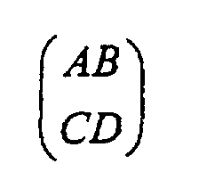
- FIG. 2b A generalized setup is shown in Figure 2b, where the single lens 2 of Figure 2a is replaced by a general optical imaging system described by an ABCD-matrix (see Siegman, "Lasers", University Science Books, pages 581 ff).
- the ABCD-matrix formulism is known both in the ray optics and paraxial optics and is used to calculate the imaging of rays as well as of paraxial beams.
- the ABCD matrix is used for imaging rays through the optical system.
- the ABCD-matrix formulism allows to image any optical ray (r, r') where r denotes the offset from the optical axis and r' the angle of the beam.
- the optical ray After having passed the optical system described by the ABCD-matrix , ( see also Fig.1) the optical ray changes its offset and angle as calculated by simple matrix calculations:
- the ABCD matrix is used for calculating the size of the laser spot 4b at the position of a first crystal 1 b.
- the laser beam incident on the angle-adjustable mirror M1 can be described in generalized parameters (p, q) instead of the parameters (r, r').
- Figure 2b alpha, beta and gamma show different possible schemes obtained following the guidelines given above.
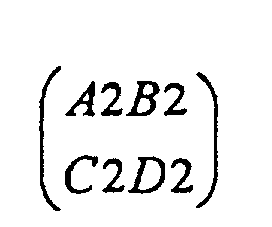
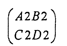
- Figure 2b beta an example is shown how two crystals in series can be illuminated by the laser beam which first passes the angle-adjustable mirror, then a first optical system described by then the first crystal 1b, followed by a second optical imaging system and then the second crystal 1c.
- Figure 2b gamma shows a simple embodiment using two lenses for the second optical imaging system
- first lens 10a is positioned at a distance L1, corresponding to its focal length, from the first crystal 1b, and the second lens 10b separated from the first lens by a distance corresponding to the sum of the focal length of the first and the second lens L1, L2, and the second crystal 1b positioned in a distance corresponding to the focal length L2 of the second lens 10b.
- L1 11 mm
- f1 11 mm
- f2 8mm
- L3 8mm.
- the laser beam properties at the second crystal 10b may also be obtained by using the same matrix for the calculation of those parameters.
- the setup of Figure 2b gamma with the above parameters can be used, for example, to generate ultraviolet laser light from pulsed infrared laser light.
- non-critically phase-matched LBO can be used as the first crystal 10a, and critically phase-matched LBO as the second crystal 10b.
- any walk-off is neglected that might occur inside the optical material between the fundamental (i.e. incident) and the frequency-converted beam, which results in the two beams being on the same axis.
- the same scheme can be used if (even strong) walk-off will result.
- the frequency-converted beam 8 and the fundamental (incident) beam 3 will still be on axis.
- the frequency-converted beam 8 travels along a different axis inside the nonlinear optical material 1a. All beams, however, will exit the material on parallel axes, as shown in Figure 3.
- the back-travelling beams 8 and 3 are combined finally in the same axis when exiting the front side of the nonlinear optical material 1a.
- the same considerations apply when the reflecting surface 7a is directly attached to the back side of the nonlinear optical material 1a, perpendicular to the axis of the incident beam 3. These considerations also apply for any kind of birefringent optical material and are not necessarily limited to nonlinear optical materials.
- the lens 3 can also be replaced by a reflective mirror with corresponding focal length.
- the lens or reflective focusing mirror does not have to be spherical, as would be most common in many applications. But it could also be a cylindrical lens or a cylindrical focusing mirror, in which case all considerations above only apply in one transverse direction.
- the lens does not have to be a plano-concave lens, as depicted in all figures for simplicity, but it could be any kind of focusing means. For example, achromatic lenses, doubletts, cylindrical lenses, parabolic mirrors, and many more would apply.
- Figure 4 shows the technical drawing of one possible setup of a simple and stable adjustable optical means, that needs only two screws.
- the adjustable optical means is machined out of a solid aluminum block. Other materials may also be suitable. The machining may be done from three sides.
- the adjustable optical means shown in Figure 4 is designed for holding an optical component 12 or a laser mirror with 12.7 mm diameter and 9.5 mm length. It is to be understood that the adjustable optical means can be made substantially smaller or larger.
- a first hole H1 holding for example the laser mirror has a diameter somewhat larger than 12.7 mm, for example 13.5 mm, except for the elevated section on which the mirror is going to sit on.
- a second hole H2, which is perpendicular to the first hole H1 divides this elevated section into four touching surfaces 11.
- the optical component when put into the hole H1, will rest on these four defined touching surfaces 11 in a definite way. Theses surfaces may be shaped differently, as for instance as point surfaces or in the form of a V-groove (Fig.4d).
- the optical component 12 may be chosen such as to have one or both of its surfaces 14 wedged (dotted line in Fig.4b). Then the rotation of the optical component 12 around its axis, as indicated in Figure 4b with the circled arrow to the right, results in a fine change of the vertical angle of the wedged surface 14. This is the way to have to achieve a fine tuning of the vertical angle on the wedged surfaces before a set screw 13a on the top of the adjustable optical means will be fixed. Once the vertical angle and the set screw 13a are fixed, the adjustable optical means can still be horizontally rotated and adjusted, and will finally be fixed to an optical platform or post (not shown) by a second screw 13b.
- the optical component 12 can, for example, be a laser mirror where the wedged surface is coated with a reflective coating for the wavelength of interest. Also, the optical component could be used in transmission rather than in reflection, in which case the surface angle can again be pre-tuned due to a wedge. Any other optical materials can be used similarly.
- FIG. 5 Another setup for an adjustable optical means is shown in Figure 5. Only the first hole H1 for holding an optical component is provided and the touching surfaces are made as two parallel sections 11b for supporting the optical component 12.
- Such a type of an adjustable optical means has the advantage of being particularly simple to manufacture. It can be manufactured by machining from two sides only.
- Figure 6 shows a third alternative for an adjustable optical means where the first hole H1' is made as a simple hole only with no supporting section protruding like in the previous two embodiments.
- This first hole H1' can then be made such that the optical component 12 will fit in tightly, with the set screw 13a holding the component in place.
- glue may be used instead or in addition to the set screw 13a. If only glue is used, this results in an adjustable optical means with a mirror which will require one single screw only for mounting the adjustable optical means onto the optical platform. Before the glue will be dry, it will still be possible to adjust the angle of the wedged surface vertically by rotating the optical component around its axis.
- This invention can be used in laser or optical systems.
- this invention may be a simple solution as to how to increase the overall lifetime of the laser or optical system.
- the beam diameter may be in the order of 100 micro meters.
- the overall area of the SESAM can be much larger than the size of the laser spot. Given a SESAM size of for example 5mm x 5mm, this will result in approximately 625 spots that can be used over the SESAM surface. This will result in 625.000 hours of operation provided that each spot will endure about 1.000 hours of operation.
- this invention may be used to search for a good spot or avoid bad spots by tilting M1 until the desired spot quality is reached.
- UV ultra violet light
- BBO can be used as the optical material in the configuration of Figure 2a.
- M1 is made reflective for both the incident green light and the back-reflected frequency-doubled ultra-violet light.
- the lens is made transmissive for both wavelengths.
- the walk-off apparent in BBO is compensated according to the scheme of figure 3.
- the dichroic mirror can be used to separate the two wavelengths.
- M1 can be made high transmissive for the UV and reflective for the incident wavelength, in which case M1 would act as the dichroic mirror. However, any tilt of M1 would then result in a change of the UV output direction.
- a cylindrical lens or a cylindrical mirror or any other focusing means that only acts in one transverse direction, this would generate an asymmetric beam inside the optical material.
- This can result in a number of advantages:
- the different beam properties in the two transverse directions can each separately be well matched to the requirements for optimum frequency conversion according to standard nonlinear optics formulas.
- the angle acceptance for frequency conversion in an optical material may be higher in the vertical transverse direction than in the horizontal direction, in which case a stronger focusing condition is preferably used in the vertical direction.
- walk-off may occur predominantly in one transverse direction, in which case the focusing condition can also be matched to the walk-off angle.
- An asymmetric beam inside a vertically squeezed nonlinear optical crystal can result in a one-dimensional heat flow which can increase the thermal load the crystal can take in comparison to radial cooling.
- the adjustable optical means described in this invention may be used in combination with the first objective of the invention.
- it may be used as adjustable optical means for the optical material in a setup such as described in Figures 1 to 3.
Landscapes
- Physics & Mathematics (AREA)
- Optics & Photonics (AREA)
- Electromagnetism (AREA)
- General Physics & Mathematics (AREA)
- Engineering & Computer Science (AREA)
- Plasma & Fusion (AREA)
- Optical Modulation, Optical Deflection, Nonlinear Optics, Optical Demodulation, Optical Logic Elements (AREA)
- Lasers (AREA)
- Mounting And Adjusting Of Optical Elements (AREA)
Abstract
Description




Alternatively, glue may be used instead or in addition to the
Claims (15)
- Laser generating system for using degradable optical materials comprisinga laser setup for generating a laser beam (3),an optical material (1a), which has limited durability under light exposure,an optical system with imaging means for imaging said laser beam (3) onto said optical material (1a), which imaging means compriseat least an optical imaging system (2) for focusing said laser beam onto the optical material (1a) andat least an optical means (M1) for changing the angle of the propagation axis of said laser beam (3),whereby said optical imaging system is positioned between said optical means (M1) and said optical material (1a), and is described by awhereby D is substantially zero.

- Laser generating system according to claim 1 characterized in that said optical material is a nonlinear optical material.
- Laser generating system according to claim 1 or 2 characterized in that said laser beam (3) is reflected back onto itself after passing said optical material (1a).
- Laser generating system according to claim 3 characterized in that said laser beam (3) is reflected back onto itself by a reflective surface (7a) on the back side of said optical material (1a).
- Laser generating system according to any one of the preceding claims comprising a dichroic mirror (9) or a polarizing beam splitter.
- Laser generating system according to one of the preceding claims, wherein said optical material (1,1b) isa semiconductor saturable absorber; ora nonlinear optical crystal used for frequency conversion such as second harmonic, third harmonic, multiple harmonic generation or optical parametric oscillation or amplification; orlithium borate (LBO), beta-barium borate (BBO), potassium titanyl phosphate (KTP), cesium lithium borate (CLBO) or periodically poled lithium niobate (PPLN).
- Laser generating system according to any one of the preceding claims, wherein said optical means (M1) is a part of a resonator of said laser setup
- Laser generating system according to claim 7, comprising an optical system.
- Laser generating system according to claim 8 comprising an optical system includingsecond imaging means for imaging said laser beam (3) onto a second optical material (1c) whereby the second imaging means compriseat least a second optical imaging system (2) for focusing said laser beam (3) onto the second optical material (1c) andat least a second optical means for changing the relative position of the propagation axis of the laser beam (3), whereby said second optical imaging system is positioned between said second optical means and said second optical material (1c), and is described by awhereby C is substantially zero.

- Laser generating system according to one of the claims 8 or 9, wherein said second optical material (1c) isa semiconductor saturable absorber; ora nonlinear optical crystal used for frequency conversion such as second harmonic, third harmonic, multiple harmonic generation or optical parametric oscillation or amplification; orlithium borate (LBO), beta-barium borate (BBO), potassium titanyl phosphate (KTP), cesium lithium borate (CLBO) or periodically poled lithium niobate (PPLN).
- Laser generating system according to any one of the claims 1 through 10, comprising adjustable optical means for an optical system includingan optical component (12) with one or two wedged surfaces (14) anda holder for said optical component (12) comprisingwherein said optical component (12) is rotatable around its axis in said recess.means for supporting said optical component (12) which supporting means comprise four defined touching surfaces (11);one recess for inserting said optical component (12);one fixing means for fixing said optical component (12) in the recess;
- Laser generating system according to claim 11, wherein the defined touching surfaces (11) are shaped in the form of V-grooves.
- Laser generating system according to claim 11 or 12, wherein said optical component (12) and said recess are substantially cylindrical.
- Laser generating system according to any one of the claims 11 through 13, wherein said optical component (12) is a laser mirror or a nonlinear material.
- Laser generating system according to any one of the claims 11 through 14, wherein said fixing means is a screw (13a)
Applications Claiming Priority (3)
| Application Number | Priority Date | Filing Date | Title |
|---|---|---|---|
| US13889599P | 1999-06-11 | 1999-06-11 | |
| US138895P | 1999-06-11 | ||
| PCT/EP2000/005203 WO2000077890A2 (en) | 1999-06-11 | 2000-06-07 | Optical system for lasers |
Publications (2)
| Publication Number | Publication Date |
|---|---|
| EP1194804A2 EP1194804A2 (en) | 2002-04-10 |
| EP1194804B1 true EP1194804B1 (en) | 2003-07-30 |
Family
ID=22484144
Family Applications (1)
| Application Number | Title | Priority Date | Filing Date |
|---|---|---|---|
| EP00940330A Expired - Lifetime EP1194804B1 (en) | 1999-06-11 | 2000-06-07 | LASER generating system |
Country Status (4)
| Country | Link |
|---|---|
| EP (1) | EP1194804B1 (en) |
| AT (1) | ATE246367T1 (en) |
| DE (1) | DE60004237T2 (en) |
| WO (1) | WO2000077890A2 (en) |
Cited By (8)
| Publication number | Priority date | Publication date | Assignee | Title |
|---|---|---|---|---|
| US8929406B2 (en) | 2013-01-24 | 2015-01-06 | Kla-Tencor Corporation | 193NM laser and inspection system |
| US9042006B2 (en) | 2012-09-11 | 2015-05-26 | Kla-Tencor Corporation | Solid state illumination source and inspection system |
| US9413134B2 (en) | 2011-07-22 | 2016-08-09 | Kla-Tencor Corporation | Multi-stage ramp-up annealing for frequency-conversion crystals |
| US9419407B2 (en) | 2014-09-25 | 2016-08-16 | Kla-Tencor Corporation | Laser assembly and inspection system using monolithic bandwidth narrowing apparatus |
| US9529182B2 (en) | 2013-02-13 | 2016-12-27 | KLA—Tencor Corporation | 193nm laser and inspection system |
| US9608399B2 (en) | 2013-03-18 | 2017-03-28 | Kla-Tencor Corporation | 193 nm laser and an inspection system using a 193 nm laser |
| US9748729B2 (en) | 2014-10-03 | 2017-08-29 | Kla-Tencor Corporation | 183NM laser and inspection system |
| US9804101B2 (en) | 2014-03-20 | 2017-10-31 | Kla-Tencor Corporation | System and method for reducing the bandwidth of a laser and an inspection system and method using a laser |
Families Citing this family (4)
| Publication number | Priority date | Publication date | Assignee | Title |
|---|---|---|---|---|
| EP1386196A1 (en) | 2001-05-08 | 2004-02-04 | Spectra Physics Lasers, Inc. | Algorithm for enhancing the lifetime of critical components in a laser system |
| FR2938935B1 (en) * | 2008-11-21 | 2011-05-06 | Eolite Systems | DEVICE FOR EXTENDING THE LIFETIME OF A NON-LINEAR OPTICAL SYSTEM SUBJECTED TO RADIATION OF AN INTENSE LASER BEAM AND NON-LINEAR OPTICAL SOURCE COMPRISING SAID DEVICE |
| US8976343B2 (en) | 2012-06-21 | 2015-03-10 | Kla-Tencor Corporation | Laser crystal degradation compensation |
| US10175555B2 (en) | 2017-01-03 | 2019-01-08 | KLA—Tencor Corporation | 183 nm CW laser and inspection system |
Family Cites Families (9)
| Publication number | Priority date | Publication date | Assignee | Title |
|---|---|---|---|---|
| US3432771A (en) * | 1964-12-18 | 1969-03-11 | Ibm | Optical scanning techniques employing an optical cavity including two reflectors and a focussing objective |
| FR2659258B1 (en) * | 1990-03-06 | 1994-10-21 | Peugeot | DEVICE FOR ADJUSTING ORIENTATION, PARTICULARLY FOR ADJUSTING THE POSITION OF A LASER BEAM. |
| IL111124A (en) * | 1994-10-02 | 1996-07-23 | Univ Ramot | Positioning devices and a method and positioning device for aligning an optical fiber with an optical beam |
| DE19515321A1 (en) * | 1995-04-20 | 1996-10-24 | Gos Ges Zur Foerderung Angewan | Tunable, adjustable stable laser light source with spectrally filtered output |
| GB2305232B (en) * | 1995-09-15 | 2000-04-19 | Pilkington Perkin Elmer Ltd | Adjustment arrangement |
| US5737132A (en) * | 1996-05-06 | 1998-04-07 | New Focus, Inc. | Flip-type mirror mount |
| US5825562A (en) * | 1997-08-18 | 1998-10-20 | Novatec Corporation | Method of continuous motion for prolong usage of optical elements under the irradiation of intensive laser beams |
| US5852519A (en) * | 1997-09-05 | 1998-12-22 | New Focus, Inc. | Positionable multi-optic holder |
| US6034804A (en) * | 1998-03-31 | 2000-03-07 | The United States Of America As Represented By The Secretary Of The Navy | Rapid, high-resolution scanning of flat and curved regions for gated optical imaging |
-
2000
- 2000-06-07 DE DE60004237T patent/DE60004237T2/en not_active Expired - Lifetime
- 2000-06-07 WO PCT/EP2000/005203 patent/WO2000077890A2/en not_active Ceased
- 2000-06-07 AT AT00940330T patent/ATE246367T1/en not_active IP Right Cessation
- 2000-06-07 EP EP00940330A patent/EP1194804B1/en not_active Expired - Lifetime
Cited By (9)
| Publication number | Priority date | Publication date | Assignee | Title |
|---|---|---|---|---|
| US9413134B2 (en) | 2011-07-22 | 2016-08-09 | Kla-Tencor Corporation | Multi-stage ramp-up annealing for frequency-conversion crystals |
| US9042006B2 (en) | 2012-09-11 | 2015-05-26 | Kla-Tencor Corporation | Solid state illumination source and inspection system |
| US8929406B2 (en) | 2013-01-24 | 2015-01-06 | Kla-Tencor Corporation | 193NM laser and inspection system |
| US9318869B2 (en) | 2013-01-24 | 2016-04-19 | Kla-Tencor Corporation | 193nm laser and inspection system |
| US9529182B2 (en) | 2013-02-13 | 2016-12-27 | KLA—Tencor Corporation | 193nm laser and inspection system |
| US9608399B2 (en) | 2013-03-18 | 2017-03-28 | Kla-Tencor Corporation | 193 nm laser and an inspection system using a 193 nm laser |
| US9804101B2 (en) | 2014-03-20 | 2017-10-31 | Kla-Tencor Corporation | System and method for reducing the bandwidth of a laser and an inspection system and method using a laser |
| US9419407B2 (en) | 2014-09-25 | 2016-08-16 | Kla-Tencor Corporation | Laser assembly and inspection system using monolithic bandwidth narrowing apparatus |
| US9748729B2 (en) | 2014-10-03 | 2017-08-29 | Kla-Tencor Corporation | 183NM laser and inspection system |
Also Published As
| Publication number | Publication date |
|---|---|
| DE60004237D1 (en) | 2003-09-04 |
| EP1194804A2 (en) | 2002-04-10 |
| WO2000077890A2 (en) | 2000-12-21 |
| WO2000077890A3 (en) | 2001-12-06 |
| DE60004237T2 (en) | 2004-04-15 |
| ATE246367T1 (en) | 2003-08-15 |
Similar Documents
| Publication | Publication Date | Title |
|---|---|---|
| US6888855B1 (en) | Optical system for lasers | |
| US6317449B1 (en) | Method and device for resonance enhancement, in particular for tunable frequency conversion of laser radiation | |
| JP5898957B2 (en) | Device for extending the lifetime of a nonlinear optical system exposed to radiation of an intense laser beam and a nonlinear light source comprising said device | |
| US5365366A (en) | Synchronously pumped sub-picosecond optical parametric oscillator | |
| JP6453844B2 (en) | High-efficiency single-pass harmonic generator for circular output beams | |
| US6714567B2 (en) | Laser light generating apparatus and optical apparatus using the same | |
| US8339697B2 (en) | Wavelength conversion laser light source and image display device | |
| KR101633154B1 (en) | Arrangement and method for the frequency conversion of laser radiation | |
| JP6640733B2 (en) | Mid-infrared Kerr-lens mode-locked laser with polycrystalline TM: II-VI material for normal incidence mounting and method for controlling parameters of polycrystalline TM: II-VI kerr-lens mode-locked laser | |
| JPH0242778A (en) | Laser resonator | |
| JP6991995B2 (en) | High efficiency laser system for 3rd harmonic generation | |
| EP1194804A2 (en) | Optical system for lasers | |
| US5068546A (en) | Solid state laser operating with frequency doubling and stabilized by an external resonator | |
| CA2391806A1 (en) | Device for the frequency conversion of a fundamental laser frequency to other frequencies | |
| WO2017004528A1 (en) | Power-scalable nonlinear optical wavelength converter | |
| JPH01286477A (en) | Annular resonant type laser device | |
| JP2023502411A (en) | Frequency converter for optimizing laser harmonic properties | |
| JP2001077449A (en) | Mode-locked solid-state laser | |
| US9543732B2 (en) | Laser wavelength conversion apparatus | |
| US6101022A (en) | High beam quality optical parametric oscillator | |
| US11563305B2 (en) | Resonantly enhanced frequency conversion with adaptive thermal-lensing compensation | |
| US6282227B1 (en) | Diode-pumped double frequency solid-state laser | |
| JP2002055368A (en) | Wavelength conversion laser device | |
| JP2000164950A (en) | Laser, laser cutter, and laser wavelength conversion method | |
| CN1115759C (en) | Laser frequency multiplier |
Legal Events
| Date | Code | Title | Description |
|---|---|---|---|
| PUAI | Public reference made under article 153(3) epc to a published international application that has entered the european phase |
Free format text: ORIGINAL CODE: 0009012 |
|
| 17P | Request for examination filed |
Effective date: 20011208 |
|
| AK | Designated contracting states |
Kind code of ref document: A2 Designated state(s): AT CH DE FR GB LI Kind code of ref document: A2 Designated state(s): AT BE CH CY DE DK ES FI FR GB GR IE IT LI LU MC NL PT SE |
|
| 17Q | First examination report despatched |
Effective date: 20020412 |
|
| RTI1 | Title (correction) |
Free format text: LASER GENERATING SYSTEM |
|
| GRAH | Despatch of communication of intention to grant a patent |
Free format text: ORIGINAL CODE: EPIDOS IGRA |
|
| RTI1 | Title (correction) |
Free format text: LASER GENERATING SYSTEM |
|
| GRAH | Despatch of communication of intention to grant a patent |
Free format text: ORIGINAL CODE: EPIDOS IGRA |
|
| GRAA | (expected) grant |
Free format text: ORIGINAL CODE: 0009210 |
|
| AK | Designated contracting states |
Designated state(s): AT CH DE FR GB LI |
|
| PG25 | Lapsed in a contracting state [announced via postgrant information from national office to epo] |
Ref country code: LI Free format text: LAPSE BECAUSE OF FAILURE TO SUBMIT A TRANSLATION OF THE DESCRIPTION OR TO PAY THE FEE WITHIN THE PRESCRIBED TIME-LIMIT Effective date: 20030730 Ref country code: AT Free format text: LAPSE BECAUSE OF FAILURE TO SUBMIT A TRANSLATION OF THE DESCRIPTION OR TO PAY THE FEE WITHIN THE PRESCRIBED TIME-LIMIT Effective date: 20030730 Ref country code: CH Free format text: LAPSE BECAUSE OF FAILURE TO SUBMIT A TRANSLATION OF THE DESCRIPTION OR TO PAY THE FEE WITHIN THE PRESCRIBED TIME-LIMIT Effective date: 20030730 |
|
| REG | Reference to a national code |
Ref country code: GB Ref legal event code: FG4D |
|
| REG | Reference to a national code |
Ref country code: CH Ref legal event code: EP |
|
| REG | Reference to a national code |
Ref country code: IE Ref legal event code: FG4D |
|
| REF | Corresponds to: |
Ref document number: 60004237 Country of ref document: DE Date of ref document: 20030904 Kind code of ref document: P |
|
| REG | Reference to a national code |
Ref country code: CH Ref legal event code: PL |
|
| ET | Fr: translation filed | ||
| PLBE | No opposition filed within time limit |
Free format text: ORIGINAL CODE: 0009261 |
|
| STAA | Information on the status of an ep patent application or granted ep patent |
Free format text: STATUS: NO OPPOSITION FILED WITHIN TIME LIMIT |
|
| 26N | No opposition filed |
Effective date: 20040504 |
|
| REG | Reference to a national code |
Ref country code: IE Ref legal event code: MM4A |
|
| REG | Reference to a national code |
Ref country code: DE Ref legal event code: R082 Ref document number: 60004237 Country of ref document: DE Representative=s name: KAMINSKI HARMANN PATENTANWAELTE EST., LI |
|
| REG | Reference to a national code |
Ref country code: GB Ref legal event code: 732E Free format text: REGISTERED BETWEEN 20110908 AND 20110914 |
|
| REG | Reference to a national code |
Ref country code: DE Ref legal event code: R081 Ref document number: 60004237 Country of ref document: DE Owner name: HIGH Q LASER GMBH, AT Free format text: FORMER OWNER: KOPF, DANIEL DR., ROETHIS, AT Effective date: 20110826 Ref country code: DE Ref legal event code: R082 Ref document number: 60004237 Country of ref document: DE Representative=s name: KAMINSKI HARMANN PATENTANWAELTE AG, LI Effective date: 20110826 Ref country code: DE Ref legal event code: R081 Ref document number: 60004237 Country of ref document: DE Owner name: HIGH Q LASER GMBH, AT Free format text: FORMER OWNER: DANIEL DR. KOPF, ROETHIS, AT Effective date: 20110826 |
|
| REG | Reference to a national code |
Ref country code: FR Ref legal event code: TP Owner name: HIGH Q TECHNOLOGIES GMBH, AT Effective date: 20110927 |
|
| REG | Reference to a national code |
Ref country code: DE Ref legal event code: R082 Ref document number: 60004237 Country of ref document: DE Representative=s name: KAMINSKI HARMANN PATENTANWAELTE AG, LI |
|
| REG | Reference to a national code |
Ref country code: DE Ref legal event code: R081 Ref document number: 60004237 Country of ref document: DE Owner name: HIGH Q LASER GMBH, AT Free format text: FORMER OWNER: HIGH Q TECHNOLOGIES GMBH, RANKWEIL, AT Effective date: 20120612 Ref country code: DE Ref legal event code: R082 Ref document number: 60004237 Country of ref document: DE Representative=s name: KAMINSKI HARMANN PATENTANWAELTE AG, LI Effective date: 20120612 |
|
| REG | Reference to a national code |
Ref country code: FR Ref legal event code: CD Owner name: HIGH Q LASER GMBH, AT Effective date: 20120906 |
|
| REG | Reference to a national code |
Ref country code: FR Ref legal event code: PLFP Year of fee payment: 16 |
|
| PGFP | Annual fee paid to national office [announced via postgrant information from national office to epo] |
Ref country code: GB Payment date: 20150622 Year of fee payment: 16 |
|
| PGFP | Annual fee paid to national office [announced via postgrant information from national office to epo] |
Ref country code: FR Payment date: 20150622 Year of fee payment: 16 |
|
| PGFP | Annual fee paid to national office [announced via postgrant information from national office to epo] |
Ref country code: DE Payment date: 20150630 Year of fee payment: 16 |
|
| REG | Reference to a national code |
Ref country code: DE Ref legal event code: R119 Ref document number: 60004237 Country of ref document: DE |
|
| GBPC | Gb: european patent ceased through non-payment of renewal fee |
Effective date: 20160607 |
|
| REG | Reference to a national code |
Ref country code: FR Ref legal event code: ST Effective date: 20170228 |
|
| PG25 | Lapsed in a contracting state [announced via postgrant information from national office to epo] |
Ref country code: FR Free format text: LAPSE BECAUSE OF NON-PAYMENT OF DUE FEES Effective date: 20160630 Ref country code: DE Free format text: LAPSE BECAUSE OF NON-PAYMENT OF DUE FEES Effective date: 20170103 |
|
| PG25 | Lapsed in a contracting state [announced via postgrant information from national office to epo] |
Ref country code: GB Free format text: LAPSE BECAUSE OF NON-PAYMENT OF DUE FEES Effective date: 20160607 |