EP1193764A1 - Integrated photodetector - Google Patents

Integrated photodetector Download PDF

Info

Publication number
EP1193764A1
EP1193764A1 EP01308358A EP01308358A EP1193764A1 EP 1193764 A1 EP1193764 A1 EP 1193764A1 EP 01308358 A EP01308358 A EP 01308358A EP 01308358 A EP01308358 A EP 01308358A EP 1193764 A1 EP1193764 A1 EP 1193764A1
Authority
EP
European Patent Office
Prior art keywords
photodetector
layer
silicon nitride
chip
emitter
Prior art date
Legal status (The legal status is an assumption and is not a legal conclusion. Google has not performed a legal analysis and makes no representation as to the accuracy of the status listed.)
Withdrawn
Application number
EP01308358A
Other languages
German (de)
French (fr)
Inventor
Danielle A. Thomas
Gilles E. Thomas
Current Assignee (The listed assignees may be inaccurate. Google has not performed a legal analysis and makes no representation or warranty as to the accuracy of the list.)
STMicroelectronics lnc USA
Original Assignee
STMicroelectronics lnc USA
SGS Thomson Microelectronics Inc
Priority date (The priority date is an assumption and is not a legal conclusion. Google has not performed a legal analysis and makes no representation as to the accuracy of the date listed.)
Filing date
Publication date
Application filed by STMicroelectronics lnc USA, SGS Thomson Microelectronics Inc filed Critical STMicroelectronics lnc USA
Publication of EP1193764A1 publication Critical patent/EP1193764A1/en
Withdrawn legal-status Critical Current

Links

Images

Classifications

    • HELECTRICITY
    • H10SEMICONDUCTOR DEVICES; ELECTRIC SOLID-STATE DEVICES NOT OTHERWISE PROVIDED FOR
    • H10FINORGANIC SEMICONDUCTOR DEVICES SENSITIVE TO INFRARED RADIATION, LIGHT, ELECTROMAGNETIC RADIATION OF SHORTER WAVELENGTH OR CORPUSCULAR RADIATION
    • H10F39/00Integrated devices, or assemblies of multiple devices, comprising at least one element covered by group H10F30/00, e.g. radiation detectors comprising photodiode arrays
    • H10F39/80Constructional details of image sensors
    • H10F39/805Coatings
    • HELECTRICITY
    • H10SEMICONDUCTOR DEVICES; ELECTRIC SOLID-STATE DEVICES NOT OTHERWISE PROVIDED FOR
    • H10FINORGANIC SEMICONDUCTOR DEVICES SENSITIVE TO INFRARED RADIATION, LIGHT, ELECTROMAGNETIC RADIATION OF SHORTER WAVELENGTH OR CORPUSCULAR RADIATION
    • H10F39/00Integrated devices, or assemblies of multiple devices, comprising at least one element covered by group H10F30/00, e.g. radiation detectors comprising photodiode arrays
    • H10F39/80Constructional details of image sensors
    • H10F39/803Pixels having integrated switching, control, storage or amplification elements

Definitions

  • the present invention generally relates to semiconductor photodetectors, and more particularly to an integrated circuit device that includes a photodetector and a process for its fabrication.
  • BiCMOS complementary metal-oxide-semiconductor FETs
  • MOSFETs field-effect transistors
  • BiCMOS complementary metal-oxide-semiconductor FETs
  • Advanced BiCMOS processes provide IC devices that operate at high frequencies suitable for high performance electronic products.
  • the incorporation of a photodetector onto a single semiconductor chip may involve modification of an existing process technology that is semiconductor chip may involve modification of an existing process technology that is compatible with the end-use application. It would be desirable, therefore, to facilitate such a process modification in a way that does not significantly change the structures and functions of basic circuit elements (transistors and capacitors), while minimizing any increase in the number and complexity of process operations.
  • a photodetector is integrated with high speed bipolar transistors and other semiconductor elements on a single chip, using advanced BiCMOS process technology.
  • the photodetector comprises a thin, light-transmissive layer disposed above a diode having a PN junction lying generally parallel to the light-transmissive layer.
  • the diode is physically isolated from other circuit elements on the same chip, and is electrically interconnected with the chip circuitry using conductive interconnects.
  • the material that forms the light-transmissive layer extends laterally over regions of the chip that include these other circuit elements, which primarily include different types of bipolar transistors.
  • the fabrication process accommodates inclusion of the photodetector structure with a minimum of photolithographic operations by incorporating the laterally extending portions of the light-transmissive layer into the structures of various transistors on the chip without degrading their characteristics.
  • FIG. 1 is a schematic vertical cross-section (not necessarily through a single plane) of a portion of a device embodying the present invention, showing part of a semiconductor chip broken away at its left and right edges from the complete chip;
  • FIG. 2A is an enlarged left-hand portion of FIG. 1 that includes a poly-emitter vertical NPN transistor;
  • FIG. 2B is an enlarged center portion of FIG. 1 that includes a vertical PNP transistor
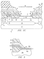
  • FIG. 2C is an enlarged right-hand portion of FIG. 1 that includes a photodetector
  • FIG. 3 is a greatly enlarged portion of FIG. 2C showing additional details of a light-transmissive layer that defines part of the disclosed photodetector.
  • FIG. 1 shows two of many possible transistors that can be fabricated on the chip 10 together with the photodetector integrated thereon.
  • the portion labeled “poly-emitter vertical NPN transistor” is shown in the enlarged view of FIG. 2A
  • the portion labeled "vertical PNP transistor” is shown in the enlarged view of FIG. 2B
  • the portion labeled "photodetector” is shown in the enlarged view of FIG. 2C.
  • the chip 10 is fabricated on a substrate 12, which preferably is lightly doped P-type silicon having a resistivity of 10 to 20 ohm-cm.
  • a substrate 12 which preferably is lightly doped P-type silicon having a resistivity of 10 to 20 ohm-cm.
  • Various buried layers are formed in the substrate 12 using conventional processing techniques, including N - buried layer 14, P + buried layers 16, and N + buried layers 18.
  • a lightly doped N-type epitaxial layer 20 is formed on the substrate 12 using a conventional epitaxial deposition process.
  • Various conventional ion implantation operations are then performed to selectively dope regions within the epitaxial layer 20. These doped regions include - field implants 22 (some of which are labeled in FIGS. 2A, 2B and 2C), P - wells 24a, 24b, and 24c, and P field implants 26.
  • Oxide isolation regions are then formed, preferably using a patterned nitride layer (not shown) to selectively grow thermal oxide to a thickness of about 6000 ⁇ . This produces a patterned field oxide layer 28. Further ion implantation operations are then performed to produce N + sinkers 30, N + contact regions 32, P + contact regions 34, P - base implant 36 (FIG. 2A), and N - base implant 38 (FIG. 2B).
  • a clean-up sequence follows that includes formation of a new, extremely thin, thermal oxide layer (not shown) in the active areas, preferably to a thickness of about 65 ⁇ .
  • an oxide layer 40a is deposited, preferably to a thickness of about 350 ⁇ . This deposition is preferably performed at about 670 ° C using TEOS (tetra-ethyl-ortho-silicate) as the source material in accordance with well-known process techniques.
  • TEOS tetra-ethyl-ortho-silicate
  • a silicon nitride (Si 3 N 4 ) layer 40b is deposited in a conventional manner to a preferred thickness of about 500 ⁇ . It will be appreciated that this layer will serve as an anti-reflective film in the completed device.
  • an additional TEOS deposition is performed to form oxide layer 40c to a preferred thickness of about 650 ⁇ .
  • Layers 40a, 40b and 40c are not shown separately in FIGS. 1, 2A, 2B and 2C because they are too thin to illustrate without great distortion. Where all three layers are present, they are referred to herein as a composite insulating layer and are designated collectively by reference numeral 40. In FIG. 3, it is shown that oxide layer 40c terminates just to the right of the edge of the field oxide layer 28, so that only layers 40a and 40b extend out over P - well 24c. Layers 40a and 40b are collectively referred to herein as light-transmissive layer 41, which is an important structural feature of the photodetector element the operation of which is described below.
  • an opening is dry cut therethrough over emitter region 36.
  • a phosphorus implantation preferably at a dose of 2.0 x 10 12 atoms/cm 2 at an energy of 240 KeV.
  • the SIC region contributes to the speed of the poly-emitter vertical NPN transistor, which has a frequency response preferably greater than 9 gigahertz.
  • polysilicon polycrystalline silicon
  • the polysilicon layer is implanted with arsenic. This ion implantation procedure not only dopes the polysilicon but also dopes a portion of the underlying silicon producing emitter contact region 44.
  • the polysilicon layer is then selectively etched to leave poly emitter 46 in place over the emitter contact region 44. It will be appreciated that the resulting structural features also contribute to high speed transistor response.
  • a glass deposition follows to form BPSG layer 48 using well-known process steps. Contact openings are then made by selective etching followed by metal deposition and patterning to form base, emitter, collector, and source contacts (labeled B, E, C and S in FIGs. 2A and 2B), and a photodetector contact (labeled P in FIG. 2C).
  • an interlevel dielectric (ILD) layer 50 is formed using conventional oxide deposition and spin-on-glass (SOG) planarization techniques. This produces a relatively flat surface atop ILD layer 50.
  • a second metal deposition and patterning sequence is performed to form metal screen plate 52. This is followed by a conventional oxide passivation deposition to produce PSG layer 54.
  • an optional polymide layer 56 is formed atop the device, which can serve to reduce the stress on the chip 10 during the subsequent packaging operation.
  • an opening or window 58 is formed down to light-transmissive layer 41 by a sequence of selective etching steps, removing portions of layers 56, 54, 50, 48. Also, as shown specifically in FIG. 3, oxide layer 40c is removed to expose nitride layer 40b, which is the top layer of light-transmissive layer 41.
  • the window 58 is rectangular in top view, having length to width ratio of 1.5, which improves the optical sensitivity.
  • the chip 10 is then packaged in a protective housing by bonding the substrate 12 to an electrode (not shown) and encapsulating the chip 10 in an IC package (not shown), which will include a transparent resin portion (not shown) over the window 58.
  • the chip 10 may include many transistors and other IC elements (capacitors and resistors) of which only two transistors are shown, together with the integrated photodetector.
  • the composite insulating layer 40 can be used as an interlevel dielectric between first and second level polysilicon layers to form a switch-mode capacitor.
  • the poly-emitter vertical NPN transistor (FIG. 2A) and the vertical PNP transistor (FIG. 2B) each operate in a well-known manner.
  • the most basic IC device with an integrated photodetector according to the invention only bipolar transistors may need to be fabricated with only slight modification to an existing BiCMOS process technology.
  • the photodetector (FIG. 2C) also operates in a well-known manner.
  • P-type region 24c and the underlying portion of the N-type epitaxial layer 20 form a PN junction or diode 60 that produces current when energized by photons passing through the light-transmissive layer.
  • Light generates electron-hole pairs inside the space-charge region of the PN junction 60.
  • positive current flows from photodetector contact P through regions 32, 30, 18 and 20 to the PN junction 60.
  • the metal contact P serves as the current drain for the diode 60.
  • the composite insulating layer 40 forms part of the transistor structures as well as contributing its lower two layers 40a and 40b (FIG. 3) to the photodetector.
  • the overall thickness and dielectric properties of the composite insulating layer 40 are chosen to provide a suitable parasitic capacitance between the edges of the poly-emitter 46 and the base region 36 of the NPN transistor (FIG. 2A).
  • the thicknesses of layers 40a and 40b of light-transmissive layer 41 (FIGS. 2C and 3) are also selected so that light-transmissive layer 41 is anti-reflective to light wavelengths the in the 650 to 750 nanometer range.
  • silicon nitride as an anti-reflective film of a photodetector is known in the art as disclosed, for example, in U.S. Patent No. 5,177,581.
  • the present invention achieves a substantial improvement in performance over such prior art devices.

Landscapes

  • Solid State Image Pick-Up Elements (AREA)
  • Light Receiving Elements (AREA)
  • Bipolar Transistors (AREA)
  • Bipolar Integrated Circuits (AREA)

Abstract

A photodetector is integrated on a single semiconductor chip with bipolar transistors including a high speed poly-emitter vertical NPN transistor. The photodetector includes a silicon nitride layer serving as an anti-reflective film. The silicon nitride layer and oxide layers on opposite sides thereof insulate edges of a polysilicon emitter from the underlying transistor regions, minimizing the parasitic capacitance between the NPN transistor's emitter and achieving a high frequency response.

Description

The present invention generally relates to semiconductor photodetectors, and more particularly to an integrated circuit device that includes a photodetector and a process for its fabrication.
Semiconductor photodetectors are well known in the art. U.S. Patent Nos. 4,670,765 and 5,177,581 disclose examples. Often such photodetectors are integrated with other circuit elements on the same semiconductor chip. U.S. Patent Nos. 5,049,733 and 5,105,090 disclose examples. Another example that is compatible with a more advanced fabrication process is disclosed in U.S. Patent No. 5,994,162. These five patents are incorporated by reference herein as background technology.
Semiconductor manufacturers have developed complex process technologies that permit fabrication of high circuit densities on a single silicon chip. Many such technologies have the flexibility of forming either bipolar transistors or field-effect transistors (FETs), or more typically, both types of transistors on the same chip. When both complementary forms of metal-oxide-semiconductor FETs (both N-channel and P-channel MOSFETs) are formed with bipolar transistors on the same chip, the generic process technology is referred to as BiCMOS. Advanced BiCMOS processes provide IC devices that operate at high frequencies suitable for high performance electronic products. The incorporation of a photodetector onto a single semiconductor chip may involve modification of an existing process technology that is semiconductor chip may involve modification of an existing process technology that is compatible with the end-use application. It would be desirable, therefore, to facilitate such a process modification in a way that does not significantly change the structures and functions of basic circuit elements (transistors and capacitors), while minimizing any increase in the number and complexity of process operations.
In accordance with a principal object of the invention, a photodetector is integrated with high speed bipolar transistors and other semiconductor elements on a single chip, using advanced BiCMOS process technology. The photodetector comprises a thin, light-transmissive layer disposed above a diode having a PN junction lying generally parallel to the light-transmissive layer. The diode is physically isolated from other circuit elements on the same chip, and is electrically interconnected with the chip circuitry using conductive interconnects. The material that forms the light-transmissive layer extends laterally over regions of the chip that include these other circuit elements, which primarily include different types of bipolar transistors. The fabrication process accommodates inclusion of the photodetector structure with a minimum of photolithographic operations by incorporating the laterally extending portions of the light-transmissive layer into the structures of various transistors on the chip without degrading their characteristics.
The novel features believed characteristic of the invention are set forth in the appended claims. The nature of the invention, however, as well as its essential features and advantages, may be understood more fully upon consideration of an illustrative embodiment, when read in conjunction with the accompanying drawings, wherein:
FIG. 1 is a schematic vertical cross-section (not necessarily through a single plane) of a portion of a device embodying the present invention, showing part of a semiconductor chip broken away at its left and right edges from the complete chip;
FIG. 2A is an enlarged left-hand portion of FIG. 1 that includes a poly-emitter vertical NPN transistor;
FIG. 2B is an enlarged center portion of FIG. 1 that includes a vertical PNP transistor;
FIG. 2C is an enlarged right-hand portion of FIG. 1 that includes a photodetector; and
FIG. 3 is a greatly enlarged portion of FIG. 2C showing additional details of a light-transmissive layer that defines part of the disclosed photodetector.
Referring initially to FIG. 1, FIG. 2A, FIG. 2B and FIG. 2C, a portion of a semiconductor chip is illustrated and designated generally by reference numeral 10. For clarity, some of the numerals used in FIGS 2A, 2B and 2C are not included in FIG. 1. FIG. 1 shows two of many possible transistors that can be fabricated on the chip 10 together with the photodetector integrated thereon. The portion labeled "poly-emitter vertical NPN transistor" is shown in the enlarged view of FIG. 2A, the portion labeled "vertical PNP transistor" is shown in the enlarged view of FIG. 2B, and the portion labeled "photodetector" is shown in the enlarged view of FIG. 2C.
The chip 10 is fabricated on a substrate 12, which preferably is lightly doped P-type silicon having a resistivity of 10 to 20 ohm-cm. Various buried layers are formed in the substrate 12 using conventional processing techniques, including N-buried layer 14, P+ buried layers 16, and N+ buried layers 18.
A lightly doped N-type epitaxial layer 20 is formed on the substrate 12 using a conventional epitaxial deposition process. Various conventional ion implantation operations are then performed to selectively dope regions within the epitaxial layer 20. These doped regions include- field implants 22 (some of which are labeled in FIGS. 2A, 2B and 2C), P- wells 24a, 24b, and 24c, and P field implants 26.
Oxide isolation regions are then formed, preferably using a patterned nitride layer (not shown) to selectively grow thermal oxide to a thickness of about 6000Å. This produces a patterned field oxide layer 28. Further ion implantation operations are then performed to produce N+ sinkers 30, N+ contact regions 32, P+ contact regions 34, P- base implant 36 (FIG. 2A), and N- base implant 38 (FIG. 2B). Preferably, a clean-up sequence follows that includes formation of a new, extremely thin, thermal oxide layer (not shown) in the active areas, preferably to a thickness of about 65Å.
Now referring to FIG. 3, an important feature of the invention will be described. First, an oxide layer 40a is deposited, preferably to a thickness of about 350Å. This deposition is preferably performed at about 670 ° C using TEOS (tetra-ethyl-ortho-silicate) as the source material in accordance with well-known process techniques. Next, a silicon nitride (Si3N4) layer 40b is deposited in a conventional manner to a preferred thickness of about 500Å. It will be appreciated that this layer will serve as an anti-reflective film in the completed device. Next, an additional TEOS deposition is performed to form oxide layer 40c to a preferred thickness of about 650Å.
Layers 40a, 40b and 40c are not shown separately in FIGS. 1, 2A, 2B and 2C because they are too thin to illustrate without great distortion. Where all three layers are present, they are referred to herein as a composite insulating layer and are designated collectively by reference numeral 40. In FIG. 3, it is shown that oxide layer 40c terminates just to the right of the edge of the field oxide layer 28, so that only layers 40a and 40b extend out over P- well 24c. Layers 40a and 40b are collectively referred to herein as light-transmissive layer 41, which is an important structural feature of the photodetector element the operation of which is described below.
Referring again to FIG. 2A, after composite insulating layer 40 has been formed, an opening is dry cut therethrough over emitter region 36. This is followed by a phosphorus implantation preferably at a dose of 2.0 x 10¹² atoms/cm2 at an energy of 240 KeV. This forms selectively implanted collector (SIC) region 42. The SIC region contributes to the speed of the poly-emitter vertical NPN transistor, which has a frequency response preferably greater than 9 gigahertz.
Then, after a clean-up operation, a deposition of polycrystalline silicon (more simply referred to as polysilicon) is performed. The polysilicon layer is implanted with arsenic. This ion implantation procedure not only dopes the polysilicon but also dopes a portion of the underlying silicon producing emitter contact region 44. The polysilicon layer is then selectively etched to leave poly emitter 46 in place over the emitter contact region 44. It will be appreciated that the resulting structural features also contribute to high speed transistor response.
A glass deposition follows to form BPSG layer 48 using well-known process steps. Contact openings are then made by selective etching followed by metal deposition and patterning to form base, emitter, collector, and source contacts (labeled B, E, C and S in FIGs. 2A and 2B), and a photodetector contact (labeled P in FIG. 2C).
Referring again to FIG. 1, an interlevel dielectric (ILD) layer 50 is formed using conventional oxide deposition and spin-on-glass (SOG) planarization techniques. This produces a relatively flat surface atop ILD layer 50. A second metal deposition and patterning sequence is performed to form metal screen plate 52. This is followed by a conventional oxide passivation deposition to produce PSG layer 54. Then, an optional polymide layer 56 is formed atop the device, which can serve to reduce the stress on the chip 10 during the subsequent packaging operation.
Referring again to FIG. 2C, an opening or window 58 is formed down to light-transmissive layer 41 by a sequence of selective etching steps, removing portions of layers 56, 54, 50, 48. Also, as shown specifically in FIG. 3, oxide layer 40c is removed to expose nitride layer 40b, which is the top layer of light-transmissive layer 41. Preferably, the window 58 is rectangular in top view, having length to width ratio of 1.5, which improves the optical sensitivity.
The chip 10 is then packaged in a protective housing by bonding the substrate 12 to an electrode (not shown) and encapsulating the chip 10 in an IC package (not shown), which will include a transparent resin portion (not shown) over the window 58. The chip 10 may include many transistors and other IC elements (capacitors and resistors) of which only two transistors are shown, together with the integrated photodetector. In a modified form of the invention in which the chip 10 includes MOS-gated elements, the composite insulating layer 40 can be used as an interlevel dielectric between first and second level polysilicon layers to form a switch-mode capacitor.
Those skilled in the art will understand without further elaboration how the illustrated structures function. The poly-emitter vertical NPN transistor (FIG. 2A) and the vertical PNP transistor (FIG. 2B) each operate in a well-known manner. For the most basic IC device with an integrated photodetector according to the invention, only bipolar transistors may need to be fabricated with only slight modification to an existing BiCMOS process technology.
The photodetector (FIG. 2C) also operates in a well-known manner. P-type region 24c and the underlying portion of the N-type epitaxial layer 20 form a PN junction or diode 60 that produces current when energized by photons passing through the light-transmissive layer. Light generates electron-hole pairs inside the space-charge region of the PN junction 60. As a result, positive current flows from photodetector contact P through regions 32, 30, 18 and 20 to the PN junction 60. In effect, the metal contact P serves as the current drain for the diode 60.
In accordance with an important feature of the invention, the composite insulating layer 40 forms part of the transistor structures as well as contributing its lower two layers 40a and 40b (FIG. 3) to the photodetector. The overall thickness and dielectric properties of the composite insulating layer 40 are chosen to provide a suitable parasitic capacitance between the edges of the poly-emitter 46 and the base region 36 of the NPN transistor (FIG. 2A). The thicknesses of layers 40a and 40b of light-transmissive layer 41 (FIGS. 2C and 3) are also selected so that light-transmissive layer 41 is anti-reflective to light wavelengths the in the 650 to 750 nanometer range. The use of silicon nitride as an anti-reflective film of a photodetector is known in the art as disclosed, for example, in U.S. Patent No. 5,177,581. The present invention achieves a substantial improvement in performance over such prior art devices.
Although a preferred embodiment of the invention has been described in detail, it is to be understood that various changes, substitutions and alterations can be made therein without departing from the spirit and scope of the invention as set forth in the appended claims.

Claims (5)

  1. An integrated circuit device formed on a single semiconductor chip, comprising:
    a substrate;
    at least one transistor supported by the substrate; and
    a photodetector supported by the substrate laterally spaced from said transistor, said photodetector having a PN junction and a hght-transmissive layer formed above the PN junction, said light-transmissive layer including an anti-reflective silicon nitride film, said silicon nitride film extending laterally to regions of the chip removed from the photodetector and forming part of an insulating layer lying over at least a portion of said transistor.
  2. An integrated circuit device formed on a single semiconductor chip, comprising:
    a plurality of transistors including at least one poly-emitter vertical NPN transistor and at least one vertical PNP transistor, said NPN transistor having base, emitter and collector regions, the emitter region including a heavily doped region formed at an upper surface of an epitaxial layer of the chip and a heavily doped polysilicon portion in contact with the heavily doped region; and
    a photodetector having a PN junction formed in the epitaxial layer and a light-transmissive layer formed thereabove on the upper surface of the epitaxial layer, said light-transmissive layer including an anti-reflective silicon nitride film, said silicon nitride film extending laterally to regions of the chip removed from the photodetector and forming part of an insulating layer lying over portions of said NPN transistor.
  3. The integrated circuit device of Claim 2 wherein said polysilicon emitter portion of said NPN transistor includes shoulder portions overlying said insulating layer, wherein the parasitic capacitance between the base and the emitter regions of said NPN transistor is determined in part by the thickness and dielectric properties of said silicon nitride film.
  4. The integrated circuit device of Claim 3 wherein said insulating layer includes said silicon nitride layer and two silicon dioxide layers on opposite sides thereof.
  5. A method of manufacturing an integrated circuit device on a single semiconductor chip, comprising:
    providing a substrate of a first conductivity type;
    forming an epitaxial layer of a second conductivity type on the substrate; and
    forming transistors and a photodetector at laterally spaced locations on the chip;
       wherein a silicon nitride layer is formed as an anti-reflective film in the structure of the photodetector, said silicon nitride layer extending laterally from said photodetector to regions of the chip that include said transistors and performing an insulating function within the structures of said transistors.
EP01308358A 2000-10-02 2001-10-01 Integrated photodetector Withdrawn EP1193764A1 (en)

Applications Claiming Priority (4)

Application Number Priority Date Filing Date Title
US67726800A 2000-10-02 2000-10-02
US677268 2000-10-02
US838909 2001-04-20
US09/838,909 US6559488B1 (en) 2000-10-02 2001-04-20 Integrated photodetector

Publications (1)

Publication Number Publication Date
EP1193764A1 true EP1193764A1 (en) 2002-04-03

Family

ID=27101754

Family Applications (1)

Application Number Title Priority Date Filing Date
EP01308358A Withdrawn EP1193764A1 (en) 2000-10-02 2001-10-01 Integrated photodetector

Country Status (3)

Country Link
US (2) US6559488B1 (en)
EP (1) EP1193764A1 (en)
JP (1) JP2002198503A (en)

Cited By (1)

* Cited by examiner, † Cited by third party
Publication number Priority date Publication date Assignee Title
WO2007147790A1 (en) * 2006-06-17 2007-12-27 X-Fab Semiconductor Foundries Ag Method for the selective antireflection coating of a semiconductor interface by a particular process implementation

Families Citing this family (13)

* Cited by examiner, † Cited by third party
Publication number Priority date Publication date Assignee Title
JP2002151729A (en) * 2000-11-13 2002-05-24 Sony Corp Semiconductor device and manufacturing method thereof
EP1544966B1 (en) * 2003-12-16 2006-11-29 Matsushita Electric Industrial Co., Ltd. Optical semiconductor device and method for fabricating the same
US7211829B2 (en) * 2004-03-01 2007-05-01 Matsushita Electric Industrial Co., Ltd Semiconductor photodetector device
KR100628238B1 (en) * 2004-12-30 2006-09-26 동부일렉트로닉스 주식회사 CMOS image sensor and its manufacturing method
DE102005007358B4 (en) * 2005-02-17 2008-05-08 Austriamicrosystems Ag Photosensitive component
US7189957B2 (en) * 2005-02-25 2007-03-13 Taiwan Semiconductor Manufacturing Company, Ltd. Methods to improve photonic performances of photo-sensitive integrated circuits
DE102007057089B4 (en) * 2006-12-22 2010-04-29 Lg Display Co., Ltd. Liquid crystal display with photosensor and manufacturing method thereof
US7709370B2 (en) * 2007-09-20 2010-05-04 International Business Machines Corporation Spin-on antireflective coating for integration of patternable dielectric materials and interconnect structures
US8618663B2 (en) 2007-09-20 2013-12-31 International Business Machines Corporation Patternable dielectric film structure with improved lithography and method of fabricating same
US8084862B2 (en) * 2007-09-20 2011-12-27 International Business Machines Corporation Interconnect structures with patternable low-k dielectrics and method of fabricating same
JP2010010472A (en) * 2008-06-27 2010-01-14 Sanyo Electric Co Ltd Semiconductor device, and method of manufacturing the same
IT1392502B1 (en) * 2008-12-31 2012-03-09 St Microelectronics Srl SENSOR INCLUDING AT LEAST ONE DOUBLE-JOINT VERTICAL PHOTODIOD INTEGRATED ON A SEMICONDUCTIVE SUBSTRATE AND ITS INTEGRATION PROCESS
US9524994B2 (en) * 2015-04-14 2016-12-20 Semiconductor Components Industries, Llc Image sensor pixels with multiple compartments

Citations (4)

* Cited by examiner, † Cited by third party
Publication number Priority date Publication date Assignee Title
US4148048A (en) * 1977-01-24 1979-04-03 Hitachi, Ltd. Solid-state imaging device
US4606115A (en) * 1985-05-14 1986-08-19 Motorola, Inc. Method of manufacturing optically sensitive semiconductor devices including anti-reflective coatings
US5994162A (en) * 1998-02-05 1999-11-30 International Business Machines Corporation Integrated circuit-compatible photo detector device and fabrication process
EP0987767A2 (en) * 1998-09-18 2000-03-22 Capella MicroSystems, Inc. An improved photodetector and device employing the photodetector for converting an optical signal into an electrical signal

Family Cites Families (7)

* Cited by examiner, † Cited by third party
Publication number Priority date Publication date Assignee Title
US4670765A (en) 1984-04-02 1987-06-02 Sharp Kabushiki Kaisha Semiconductor photodetector element
JPH0748559B2 (en) 1988-11-30 1995-05-24 シャープ株式会社 Semiconductor device
JPH0785310B2 (en) 1989-04-07 1995-09-13 シャープ株式会社 Photodetector with built-in signal processing circuit
JP2878376B2 (en) * 1990-02-28 1999-04-05 キヤノン株式会社 Photoelectric conversion device
JP2678400B2 (en) 1990-11-14 1997-11-17 シャープ株式会社 Photodetector with built-in circuit
JP3170463B2 (en) * 1996-09-30 2001-05-28 シャープ株式会社 Photodetector with built-in circuit
WO1999039391A1 (en) * 1998-01-30 1999-08-05 Hamamatsu Photonics K.K. LIGHT-RECEIVING SEMICONDUCTOR DEVICE WITH BUIT-IN BiCMOS AND AVALANCHE PHOTODIODE

Patent Citations (4)

* Cited by examiner, † Cited by third party
Publication number Priority date Publication date Assignee Title
US4148048A (en) * 1977-01-24 1979-04-03 Hitachi, Ltd. Solid-state imaging device
US4606115A (en) * 1985-05-14 1986-08-19 Motorola, Inc. Method of manufacturing optically sensitive semiconductor devices including anti-reflective coatings
US5994162A (en) * 1998-02-05 1999-11-30 International Business Machines Corporation Integrated circuit-compatible photo detector device and fabrication process
EP0987767A2 (en) * 1998-09-18 2000-03-22 Capella MicroSystems, Inc. An improved photodetector and device employing the photodetector for converting an optical signal into an electrical signal

Cited By (1)

* Cited by examiner, † Cited by third party
Publication number Priority date Publication date Assignee Title
WO2007147790A1 (en) * 2006-06-17 2007-12-27 X-Fab Semiconductor Foundries Ag Method for the selective antireflection coating of a semiconductor interface by a particular process implementation

Also Published As

Publication number Publication date
US6559488B1 (en) 2003-05-06
JP2002198503A (en) 2002-07-12
US6803249B2 (en) 2004-10-12
US20030143786A1 (en) 2003-07-31

Similar Documents

Publication Publication Date Title
US6191457B1 (en) Integrated circuit structure having a bipolar transistor with a thick base oxide and a field effect transistor with a thin gate oxide
JP5281620B2 (en) Method of manufacturing integrated circuit structure with pin diode
US6559488B1 (en) Integrated photodetector
US6743652B2 (en) Method for making an integrated circuit device including photodiodes
US7732835B2 (en) Vertical P-N junction device and method of forming same
US6051456A (en) Semiconductor component and method of manufacture
US6580109B1 (en) Integrated circuit device including two types of photodiodes
US7192826B2 (en) Semiconductor device and process for fabrication thereof
US6576506B2 (en) Electrostatic discharge protection in double diffused MOS transistors
US5087954A (en) Mos-type integrated circuit
CN113451426A (en) Photodetector with adjacent anode-cathode pairs
US6809396B2 (en) Integrated circuit with a high speed narrow base width vertical PNP transistor
JPWO2002056381A1 (en) Semiconductor device and manufacturing method thereof
KR100486112B1 (en) Method for fabricating a BiCMOS transistor
JP3099917B2 (en) Field effect transistor
KR100731087B1 (en) Bi-SMOS device and its manufacturing method
JP3247106B2 (en) Manufacturing method and structure of integrated circuit
KR100342870B1 (en) Method for forming multiplex semiconductor device
EP1061572A1 (en) Intergrated stucture for radio frequency applications
KR20030045941A (en) Bipolar device and method of fabricating the same
JP2002319698A (en) Semiconductor device and manufacturing method thereof
WO1996024161A1 (en) Electronic device and process for making same
JP2003264272A (en) Optical semiconductor integrated circuit device and method of manufacturing the same
JPH04151871A (en) Semiconductor device
KR20030047513A (en) Bipolar device and method of fabricating the same

Legal Events

Date Code Title Description
PUAI Public reference made under article 153(3) epc to a published international application that has entered the european phase

Free format text: ORIGINAL CODE: 0009012

AK Designated contracting states

Kind code of ref document: A1

Designated state(s): AT BE CH CY DE DK ES FI FR GB GR IE IT LI LU MC NL PT SE TR

Kind code of ref document: A1

Designated state(s): DE FR GB IT

AX Request for extension of the european patent

Free format text: AL;LT;LV;MK;RO;SI

17P Request for examination filed

Effective date: 20020927

AKX Designation fees paid

Free format text: DE FR GB IT

STAA Information on the status of an ep patent application or granted ep patent

Free format text: STATUS: THE APPLICATION IS DEEMED TO BE WITHDRAWN

18D Application deemed to be withdrawn

Effective date: 20070501