EP1193638A2 - IC card connector - Google Patents
IC card connector Download PDFInfo
- Publication number
- EP1193638A2 EP1193638A2 EP01123463A EP01123463A EP1193638A2 EP 1193638 A2 EP1193638 A2 EP 1193638A2 EP 01123463 A EP01123463 A EP 01123463A EP 01123463 A EP01123463 A EP 01123463A EP 1193638 A2 EP1193638 A2 EP 1193638A2
- Authority
- EP
- European Patent Office
- Prior art keywords
- contact
- card
- parts
- connector terminals
- contact terminal
- Prior art date
- Legal status (The legal status is an assumption and is not a legal conclusion. Google has not performed a legal analysis and makes no representation as to the accuracy of the status listed.)
- Withdrawn
Links
Images


Classifications
-
- H—ELECTRICITY
- H01—ELECTRIC ELEMENTS
- H01R—ELECTRICALLY-CONDUCTIVE CONNECTIONS; STRUCTURAL ASSOCIATIONS OF A PLURALITY OF MUTUALLY-INSULATED ELECTRICAL CONNECTING ELEMENTS; COUPLING DEVICES; CURRENT COLLECTORS
- H01R12/00—Structural associations of a plurality of mutually-insulated electrical connecting elements, specially adapted for printed circuits, e.g. printed circuit boards [PCB], flat or ribbon cables, or like generally planar structures, e.g. terminal strips, terminal blocks; Coupling devices specially adapted for printed circuits, flat or ribbon cables, or like generally planar structures; Terminals specially adapted for contact with, or insertion into, printed circuits, flat or ribbon cables, or like generally planar structures
- H01R12/70—Coupling devices
- H01R12/71—Coupling devices for rigid printing circuits or like structures
-
- G—PHYSICS
- G06—COMPUTING OR CALCULATING; COUNTING
- G06K—GRAPHICAL DATA READING; PRESENTATION OF DATA; RECORD CARRIERS; HANDLING RECORD CARRIERS
- G06K7/00—Methods or arrangements for sensing record carriers, e.g. for reading patterns
- G06K7/0013—Methods or arrangements for sensing record carriers, e.g. for reading patterns by galvanic contacts, e.g. card connectors for ISO-7816 compliant smart cards or memory cards, e.g. SD card readers
- G06K7/0021—Methods or arrangements for sensing record carriers, e.g. for reading patterns by galvanic contacts, e.g. card connectors for ISO-7816 compliant smart cards or memory cards, e.g. SD card readers for reading/sensing record carriers having surface contacts
Definitions
- the present invention relates to the construction of a card connector used with an IC card used as a storage medium of a personal computer or the like, and used with a compact flash (CF) card used in electronic equipment such as digital cameras.
- CF compact flash
- An IC card connector is generally used as an additional recording apparatus of personal computers and the like.
- the IC card is widely used as a storage medium of the IC card connector.
- the IC card is mounted in the IC card connector to perform writing and reading of necessary information.
- Well-known IC card connectors have a locking mechanism that locks an IC card in a mounting position when it is inserted, and performs unlocking to eject it from the mounting position when it is ejected.
- the locking mechanism comprises a heart-shaped lock cam provided in a frame having an IC card housing recess, and a lock pin engaged in the lock cam at one end thereof and rotatably supported by a sliding member at another end thereof, wherein the sliding member is moved in an insertion direction as an IC card is inserted, whereby one end part of the lock pin slides in the lock cam to perform locking and unlocking.
- the lock pin slides within the lock cam and the IC card is temporarily subjected to overstroke, then locked in a mounting position.
- the IC card locked in the mounting position is temporarily pressed (overstroke) in the insertion direction, whereby the lock pin is disengaged from a lock part of the lock cam and the IC card is ejected in an ejection direction by the energizing force of a coil spring energizing the sliding member in the ejection direction.
- contact positions of contact parts of the connector terminals with the contact terminal parts when the IC card is in the mounting position are set on the rear end side of the contact terminal parts, when the IC card temporarily moves in the card insertion direction (toward the depth), since the contact parts of the connector terminals will come off the contact terminal parts, usually, contact positions of contact parts with the contact terminal parts when the IC card is in the mounting position are preferably set on the tip side of the contact terminal parts so that the contact between the contact terminal parts and the contact parts does not become unstable.
- contact positions of contact parts of the connector terminals with the contact terminal parts when the IC card is in the mounting position must be set on the rear end side of the contact terminal parts, posing the problem that contact positions of contact parts of the connector terminals with the contact terminal parts when the IC card is in the mounting position cannot be set on the tip side of the contact terminal parts.
- the present invention has been made to solve the above-described problems and provides a card connector capable of preventing contact parts of connector terminals from coming off card contact terminal parts due to overstroke after the contact parts contact the card contact terminal parts when the card is mounted.
- a card connector that comprises a housing in which a card at one end of which plural contact terminal parts are juxtaposed is mounted, and plural connector terminals, placed at one end of a card housing recess of the housing, having contact parts connected with the contact terminal parts as the card is inserted, wherein the housing is disposed with a first contact part and a second contact part which are different from each other in placement position in a card insertion direction, correspondingly to at least one of the contact terminal parts, and wherein when the card is inserted or ejected, as long as the card is further subjected to overstroke in the insertion direction from a card mounting position, at least one of the first contact part and the second contact part is formed so as to always contact the one contact terminal part.
- the card connector wherein the first contact part and the second contact part are formed by dividing a tip of one of the plural connector terminals.
- the card connector wherein the first contact part is formed longer in the card insertion direction than the second contact part and placed on the card insertion port side, and wherein when the distance between the first contact part and the second contact part is A, the distance from a contact position of the first contact part with the contact terminal part to the card insertion port side edge of the contact terminal part is B when the card is in a mounting position, the length of the contact terminal part in a card insertion direction is L, and an overstroke amount of the card is S, a relation of L > A > S - B is satisfied among them.
- the card connector wherein the first contact part and the second contact part are formed by dividing a tip of one of the plural connector terminals to two branches.
- the card connector wherein the connector terminals having the first and second contact parts are ground or power connector terminals.
- FIGS. 1 to 10 one embodiment of the present invention is shown in FIGS. 1 to 10;
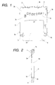
- FIG. 1 is a plan view of a card connector;
- FIG. 2 is a side view of the same;
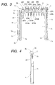
- FIG. 3 is a plan view of a housing;
- FIG. 4 is a side view of the same;
- FIG. 5 is a plan view of an IC card;
- FIG. 6 illustrates the states of contact between contact terminal parts and contact parts of connector terminals when an IC card is mounted;
- FIG. 7 illustrates the state of contact between contact terminal parts and contact parts at the time of overstroke;
- FIG. 8 illustrates the states of contact between contact terminal parts and contact parts of connector terminals when another IC card is mounted;
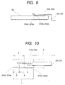
- FIG. 9 illustrates the state of contact between contact terminal parts and contact parts at the time of overstroke; and
- FIG. 10 is a simple relationship diagram showing the state of contact between contact terminal parts, and first and second contact parts of connector terminals when an IC card is mounted, and at the time of overstroke
- a housing 1 is made of an insulating material such as synthetic resin and formed into a substantial U character shape.
- a header part 1a in which plural connector terminals 2 made of a conductive metallic material are juxtaposed is provided, and at both ends of the header part 1a, guide frames 1b for guiding insertion of an IC card 4 described later are formed in opposed relation to each other.
- a portion surrounded by the header part 1a and the guide frames 1b forms a housing part 1c of the IC card 4 described later, and the connector terminals 2 juxtaposed in the header part 1a are formed projectingly to the housing part 1c.
- the plural connector terminals 2 each are formed of a flat base 2a, and a connection strip 2b and a contact strip 2c which are formed bent to a substantial Z shape in a direction facing each other from the base 2a.
- the connector terminals 2 are secured with the bases 2a engaged in the engagement slots 1d provided in the header part 1a of the housing 1, and the connection strips 2b formed at one end of the bases 2a are disposed projectingly outward from the bottom of an outside face of the header part 1a.
- the connection strips 2b are soldered with circuit patterns on external circuit boards of electronic equipment to transmit signals.
- the contact strips 2c formed at another end of the bases 2a are disposed projectingly to the housing part 1c of the IC card 4 from an upper face of an inner side of the header part 1a. At the tip of the contact strips 2c, a contact part 2d connected to contact terminal parts 5 of the IC card 4 described later is formed.
- the plural contact strips 2c are juxtaposed at intervals corresponding to the intervals of contact terminal parts 5 of the IC card 4 described later; in this case, as shown in FIG. 3, two contact strips 208c and 209c are formed at a somewhat short interval.
- the fourth and fifth contact strips 204c and 205c from the left are divided to two branches at the tips thereof at which first contact part 204da or 205da, and second contact part 204db or 205db are respectively formed.
- the first contact part 204da or 205da, and the second contact part 204db or 205db are formed so as to be placed differently from each other in an IC card insertion direction; as shown in FIG.
- the first contact part 204da and 205da are formed forwarder (toward an insertion port) in an IC card insertion direction than the second contact parts 204db and 205db.
- the contact strips 204c and 205c are disposed so that the fork-tailed first contact part 204da or 205da and second contact part 204db or 205db correspond to one contact terminal part 5 of the IC card 4.
- the first contact part 204da or 205da, and the second contact part 204db or 205db are provided in the connector terminals 204 and 205, respectively.
- the connector terminals 204 and 205 serve as ground or power connector terminals.
- the contact strips 204c and 205c of the ground or power connector terminals 204 and 205 are different in length from contact strips 202c and 203c of other connector terminals 202 and 203 for signal lines, and the contact strips 204c and 205c of the ground or power connector terminals 204 and 205 are formed longer in an IC card 4 insertion direction than the contact strips 202c and 203c of the connector terminals 202 and 203 for signal lines.
- the first contact parts 204da and 205da of the ground or power connector terminals 204 and 205, and the contact parts 202d and 203d of the connector terminals 202 and 203 for signal lines are formed so as to be placed differently from each other in an IC card 4 insertion direction so that, when the IC card 4 is mounted, the contact terminal parts 5 of the IC card 4 are connected with the first contact parts 204da and 205da of the ground or power connector terminals 204 and 205, then with the contact parts 202d and 203d of the connector terminals 202 and 203 for signal lines.
- the first contact part 204da or 205da, and the second contact part 204db or 205db of the ground or power connector terminals 204 and 205 are disposed, and the first and second contact parts are placed differently from each other in an IC card insertion direction.
- first contact part 204da or 205da, and the second contact part 204db or 205db are formed by dividing the respective tips of the connector terminals 204 and 205 to two branches, contact pressure on the contact parts can be equated, stabilizing contact.
- the connector terminals 204 and 205 are ground or power connector terminals, which must contact earliest the contact terminal part 5 during sequence operation. Therefore, by forming the tips of the connector terminals 204 and 205 so as to fork into two branches, when the IC card is in a mounting position, the first contact parts 204da and 205da can be effectively placed on the rear end side of the contact terminal part 5.
- the first contact parts 204da and 205da can be placed on the rear end side of the contact terminal part 5, they can be adequately distant from the contact parts 202d and 203d of other connector terminals 202 and 203 for signal lines to be subjected to sequence operation.
- the guide frames 1b each are provided with a guide groove 1e for guiding a side face of an IC card 4 described later to the housing part 1c when it is inserted.
- One of the guide frames 1b is provided with a heart-shaped lock cam 1g having a locking part 1f for locking a not-shown sliding member for guiding the IC card 4 in a housing position of IC card 4, and a spring housing part lh for housing a coil spring (not shown), which is an energizing member for energizing the sliding member in an ejection direction.
- Another guide frame 1b is provided with a switch housing part 1i for housing a not-shown write protect switch (detection switch for inhibiting writing) .
- a cover member 3 is made of a conductive metallic material and formed into a substantial U shape, and is formed of a flat upper plate 3a and opposing side plates 3b.
- the upper plate 3a is provided with plural window holes 3c corresponding to the contact strips 2c, and has an opening 3d provided in an IC card 4 insertion side.
- the side plates 3b are provided with a ground terminal 3e, which is connected to a ground pattern of a circuit board of electronic equipment not shown to shield the IC card 4 and card connectors.
- the cover member 3 is engaged in the housing 1 so as to cover the header part 1a and the connector terminals 2 of the housing 1.
- the IC card 4 internally houses an integrated circuit (IC) and is widely used as a recording medium.
- IC integrated circuit
- the plural contact terminal parts 5 include contact terminal parts 5a for signal lines used to transmit data, and contact terminal parts 5b for ground and power use; in this case, usually, one of the contact terminal parts 5a for signal lines is shared with a contact terminal for detecting a card.
- the second contact terminal part 5 from the left is a contact terminal part 502a for signal line which is shared with a contact terminal for detecting a card
- the fourth and fifth contact terminal parts 5 from the left are contact terminal parts 504b and 505b for ground or power use.
- the IC card 4 is provided with an inclined notch 4a at a corner of the area in which the contact terminal parts 5 are formed. By engaging a not-shown sliding member in the notch 4a, the sliding member can move in an insertion direction as the IC card 4 is inserted.
- a concave groove 4b which is an identification part indicating inhibition of writing to the IC card, is formed and provided with a slidable projection 4c. By sliding the projection 4c, the concave groove 4b can be changed in position so that whether to inhibit or permit writing to the IC card can be changed according to the position.
- the IC card 4 is inserted from the opening side of the housing part 1c of the housing 1.
- the notch 4a of the IC card 4 is engaged with a not-shown sliding member, the sliding member is moved in an insertion direction along with the IC card 4, and a not-shown lock pin slides within the lock cam 1g and is locked in the locking part 1f after overstroke.
- the IC card 4 is mounted in the housing position.
- the contact terminal parts 5 provided at the tip of the IC card 4 are connected with the contact strips 2c of the connector terminals 2 juxtaposed in the header part 1a.
- the ground or power contact terminal parts 504b and 505b (the fourth and fifth from the left in FIG. 5) of the contact terminal parts 5 correspond to the ground or power connector terminals 204 and 205 (the fourth and fifth from the left in FIG. 5)
- the first contact part 204da or 205da and the second contact part 204db or 205db of the ground or power connector terminals 204 and 205 are connected to the ground or power contact terminal parts 504b and 505b.
- FIGS. 6 and 8 show the states in which IC cards 401 and 402 of different types are used, wherein the IC cards 401 and 402 are somewhat different in the position in which the contact terminal parts 5 are placed. In this case, in an IC card mounting position, stable contact is maintained between the contact terminal parts 5 and the contact parts 2d of the connector terminals 2. However, as shown in FIGS. 7 and 9, during overstroke of the IC cards, in the case of the IC card 401 (FIG. 7), both the first contact parts 204da and 205da, and the second contact parts 204db and 205db of the ground or power connector terminals 204 and 205 contact the contact terminal parts 5, while, in the case of the IC card 402 (FIG. 9), although the second contact parts 204db and 205db contact the contact terminal parts 5, the first contact parts 204da and 205da come off rear ends of the contact terminal parts 5 and are out of contact with the contact terminal parts 5.
- the first contact parts 204da and 205da (FIGS. 6C and 8C) of the ground or power connector terminals 204 and 205, and the contact parts 202d (FIGS. 6 and 8) and 203d (FIGS. 6B and 8B) of the connector terminals 202 and 203 for signal lines must be subjected to sequence operation, they are formed so as to be placed in different positions in an insertion direction (indicated by L1 and L2 in FIGS. 6 and 8) in an IC card mounting position. Since the ground or power connector terminals 204 and 205 must contact earliest the contact terminal part 5 during sequence operation, the first contact parts 204da and 205da are placed on the rear end side of the contact terminal parts 5.
- FIG. 10 is a relationship diagram showing the state of contact between the contact terminal part 5, and the first contact part 204da or 205da and the second contact part 204db or 205db of the ground or power connector terminals 204 and 205, wherein the first contact parts 204da and 205da are formed longer in a card insertion direction (arrow X) than the second contact parts 204db and 205db, and are placed on the side of a port through which the IC card 4 is inserted.
- the distance from a contact position of the first contact part 204da or 205da with the contact terminal part 5 to the IC card 4 insertion port side edge of the contact terminal part 5 is B when the IC card 4 is in a mounting position
- the length of the contact terminal part 5 in an IC card 4 insertion direction is L
- an overstroke amount of the IC card 4 is S
- L is a default value (card specifications).
- the second contact part 204db or 205db keeps contact with the contact terminal part 5 without fail, so that constantly stable contact is obtained.
- the first contact part 204da or 205da and the second contact part 204db or 205db of the ground or power connector terminals 204 and 205 are disposed, and the first and second contact parts are placed differently from each other in an IC card insertion direction.
- the contact strips 204c and 205c of the ground or power connector terminals 204 and 205 are formed longer in an IC card 4 insertion direction than the contact strips 202c and 203c of the connector terminals 202 and 203 for signal lines, and the first contact parts 204da and 205da of the ground or power connector terminals 204 and 205, and the contact parts 202d and 203d of the connector terminals 202 and 203 for signal lines are formed so as to be placed differently from each other in an IC card 4 insertion direction. Therefore, as the IC card 4 is inserted, the ground or power contact terminals 504b and 505b first contact the first contact parts 204da and 205da of the ground or power connector terminals 204 and 205. As the IC card 4 is further inserted, they contact the contact parts 202d and 203d of the connector terminals 202 and 203 for signal lines.
- a not-shown lock pin is disengaged from the locking part 1f by temporarily pressing (overstroke) the IC card 4 in the insertion direction.
- the pressing in the insertion direction causes the sliding member to be moved in the IC card insertion direction along with the movement of the IC card 4, at which time, with the lock pin disengaged from the locking part 1f, the IC card 4 is ejected to an initial position by the energizing force of a not-shown coil spring.
- the present invention is not limited to the embodiment; without dividing the tip to two branches, a slit part of a U-shape may be provided in the middle of a connector terminal to use one of two parts divided by the slit part as a second contact part 204db or 205db.
- two different connector terminals may be respectively provided with the first contact part 204da or 205da and the second contact part 204db or 205db. At this time, the first contact part and the second contact part may be electrically connected on an external circuit board.
- first contact part 204da or 205da and the second contact part 204db or 205db are respectively disposed independently for one contact terminal part 5, one of the contact parts contacts the contact terminal part regardless of vibration, increasing the reliability of contact.
- the housing is disposed with a first contact part and a second contact part which are different from each other in placement position in a card insertion direction, correspondingly to one of contact terminal parts disposed in a card, and when the card is inserted or ejected, as long as the card is further subjected to overstroke in the insertion direction from a card mounting position, at least one of the first contact part and the second contact part is formed so as to always contact one contact terminal part.
- the first contact part and the second contact part are formed by dividing the tip of one of plural connector terminals, the construction of the card connector is simplified and workability is increased.
- the first contact part is formed longer in the card insertion direction than the second contact part and placed on the card insertion port side, and when the distance between the first contact part and the second contact part is A, the distance from a contact position of the first contact part with the contact terminal part to the card insertion port side edge of the contact terminal part is B when the card is in a mounting position, the length of the contact terminal part in a card insertion direction is L, and an overstroke amount of the card is S, a relation of L > A > S - B is satisfied among them.
- the second contact part contacts the contact terminal part without fail, providing constantly stable contact.
- first contact part and the second contact part are formed by dividing the tip of one of the plural connector terminals to two branches, contact pressure on the contact parts can be equated, contributing to the stability of contact.
- the connector terminals having the first and second contact parts are ground or power connector terminals, which must contact earliest the contact terminal parts during sequence operation. Therefore, when the card is in a mounting position, the first contact part can be effectively placed on the rear end side of the contact terminal part.
Landscapes
- Engineering & Computer Science (AREA)
- Artificial Intelligence (AREA)
- Computer Vision & Pattern Recognition (AREA)
- Physics & Mathematics (AREA)
- General Physics & Mathematics (AREA)
- Theoretical Computer Science (AREA)
- Coupling Device And Connection With Printed Circuit (AREA)
- Credit Cards Or The Like (AREA)
Abstract
Description
- The present invention relates to the construction of a card connector used with an IC card used as a storage medium of a personal computer or the like, and used with a compact flash (CF) card used in electronic equipment such as digital cameras.
- An IC card connector is generally used as an additional recording apparatus of personal computers and the like. The IC card is widely used as a storage medium of the IC card connector.
- The IC card is mounted in the IC card connector to perform writing and reading of necessary information. Well-known IC card connectors have a locking mechanism that locks an IC card in a mounting position when it is inserted, and performs unlocking to eject it from the mounting position when it is ejected.
- The locking mechanism comprises a heart-shaped lock cam provided in a frame having an IC card housing recess, and a lock pin engaged in the lock cam at one end thereof and rotatably supported by a sliding member at another end thereof, wherein the sliding member is moved in an insertion direction as an IC card is inserted, whereby one end part of the lock pin slides in the lock cam to perform locking and unlocking.
- In the locking mechanism, as the IC card is moved in an insertion direction, the lock pin slides within the lock cam and the IC card is temporarily subjected to overstroke, then locked in a mounting position. To unlock the IC card, the IC card locked in the mounting position is temporarily pressed (overstroke) in the insertion direction, whereby the lock pin is disengaged from a lock part of the lock cam and the IC card is ejected in an ejection direction by the energizing force of a coil spring energizing the sliding member in the ejection direction.
- In the construction of the above-described conventional IC card connector, to eject the IC card from the mounting position, it must be temporarily pressed (overstroke) in the insertion direction. Thereby, when the IC card is inserted or ejected, it is temporarily moved in the card insertion direction (toward the depth) from the mounting position by the overstroke, then again returns to the mounting position, and inevitably, the contact parts of connector terminals provided in a housing temporarily slide to rear ends of contact terminal parts of the IC card and again are slid to the tips thereof. Hence, if contact positions of contact parts of the connector terminals with the contact terminal parts when the IC card is in the mounting position are set on the rear end side of the contact terminal parts, when the IC card temporarily moves in the card insertion direction (toward the depth), since the contact parts of the connector terminals will come off the contact terminal parts, usually, contact positions of contact parts with the contact terminal parts when the IC card is in the mounting position are preferably set on the tip side of the contact terminal parts so that the contact between the contact terminal parts and the contact parts does not become unstable.
- However, for example, in the case where two types of IC cards different in the layout of contact terminal parts are used by one connector, and the case where sequence operation (time difference is provided for contacting timing) is required because of a relation with other contact terminal parts within an IC card), contact positions of contact parts of the connector terminals with the contact terminal parts when the IC card is in the mounting position must be set on the rear end side of the contact terminal parts, posing the problem that contact positions of contact parts of the connector terminals with the contact terminal parts when the IC card is in the mounting position cannot be set on the tip side of the contact terminal parts.
- Therefore, the present invention has been made to solve the above-described problems and provides a card connector capable of preventing contact parts of connector terminals from coming off card contact terminal parts due to overstroke after the contact parts contact the card contact terminal parts when the card is mounted.
- To solve the above-described problems, as first means of the present invention, there is provided a card connector that comprises a housing in which a card at one end of which plural contact terminal parts are juxtaposed is mounted, and plural connector terminals, placed at one end of a card housing recess of the housing, having contact parts connected with the contact terminal parts as the card is inserted, wherein the housing is disposed with a first contact part and a second contact part which are different from each other in placement position in a card insertion direction, correspondingly to at least one of the contact terminal parts, and wherein when the card is inserted or ejected, as long as the card is further subjected to overstroke in the insertion direction from a card mounting position, at least one of the first contact part and the second contact part is formed so as to always contact the one contact terminal part.
- As second means, there is provided the card connector, wherein the first contact part and the second contact part are formed by dividing a tip of one of the plural connector terminals.
- As third means, there is provided the card connector, wherein the first contact part is formed longer in the card insertion direction than the second contact part and placed on the card insertion port side, and wherein when the distance between the first contact part and the second contact part is A, the distance from a contact position of the first contact part with the contact terminal part to the card insertion port side edge of the contact terminal part is B when the card is in a mounting position, the length of the contact terminal part in a card insertion direction is L, and an overstroke amount of the card is S, a relation of L > A > S - B is satisfied among them.
- As fourth means, there is provided the card connector, wherein the first contact part and the second contact part are formed by dividing a tip of one of the plural connector terminals to two branches.
- As fifth means, there is provided the card connector, wherein the connector terminals having the first and second contact parts are ground or power connector terminals.
- Preferred embodiments of the present invention will be described in detail based on the followings, wherein:
- FIG. 1 is a plan view of a card connector according to a first embodiment of the present invention;
- FIG. 2 is a side view of the same card connector;
- FIG. 3 is a plan view of a housing of the card connector;
- FIG. 4 is a side view of the same housing;
- FIG. 5 is a plan view of an IC card of the present invention;
- FIG. 6 illustrates the states of contact between contact terminal parts and contact parts of connector terminals when an IC card is mounted;
- FIG. 7 illustrates the state of contact between contact terminal parts and contact parts at the time of overstroke;
- FIG. 8 illustrates the states of contact between contact terminal parts and contact parts of connector terminals when another IC card is mounted;
- FIG. 9 illustrates the state of contact between contact terminal parts and contact parts at the time of overstroke; and
- FIG. 10 is a simple relationship diagram showing the state of contact between a contact terminal part, and first and second contact parts of connector terminals when an IC card is mounted, and at the time of overstroke.
-
- Hereinafter, one embodiment of the present invention is shown in FIGS. 1 to 10; FIG. 1 is a plan view of a card connector; FIG. 2 is a side view of the same; FIG. 3 is a plan view of a housing; FIG. 4 is a side view of the same; FIG. 5 is a plan view of an IC card; FIG. 6 illustrates the states of contact between contact terminal parts and contact parts of connector terminals when an IC card is mounted; FIG. 7 illustrates the state of contact between contact terminal parts and contact parts at the time of overstroke; FIG. 8 illustrates the states of contact between contact terminal parts and contact parts of connector terminals when another IC card is mounted; FIG. 9 illustrates the state of contact between contact terminal parts and contact parts at the time of overstroke; and FIG. 10 is a simple relationship diagram showing the state of contact between contact terminal parts, and first and second contact parts of connector terminals when an IC card is mounted, and at the time of overstroke.
- In the drawings, a
housing 1 is made of an insulating material such as synthetic resin and formed into a substantial U character shape. At the center of thehousing 1, aheader part 1a in whichplural connector terminals 2 made of a conductive metallic material are juxtaposed is provided, and at both ends of theheader part 1a,guide frames 1b for guiding insertion of anIC card 4 described later are formed in opposed relation to each other. A portion surrounded by theheader part 1a and theguide frames 1b forms ahousing part 1c of theIC card 4 described later, and theconnector terminals 2 juxtaposed in theheader part 1a are formed projectingly to thehousing part 1c. - The
plural connector terminals 2 each are formed of aflat base 2a, and aconnection strip 2b and acontact strip 2c which are formed bent to a substantial Z shape in a direction facing each other from thebase 2a. Theconnector terminals 2 are secured with thebases 2a engaged in theengagement slots 1d provided in theheader part 1a of thehousing 1, and theconnection strips 2b formed at one end of thebases 2a are disposed projectingly outward from the bottom of an outside face of theheader part 1a. Theconnection strips 2b are soldered with circuit patterns on external circuit boards of electronic equipment to transmit signals. Thecontact strips 2c formed at another end of thebases 2a are disposed projectingly to thehousing part 1c of theIC card 4 from an upper face of an inner side of theheader part 1a. At the tip of thecontact strips 2c, acontact part 2d connected to contact terminal parts 5 of theIC card 4 described later is formed. - The
plural contact strips 2c are juxtaposed at intervals corresponding to the intervals of contact terminal parts 5 of theIC card 4 described later; in this case, as shown in FIG. 3, twocontact strips IC card 4. - The first contact part 204da or 205da, and the second contact part 204db or 205db are provided in the
connector terminals connector terminals power connector terminals other connector terminals power connector terminals IC card 4 insertion direction than the contact strips 202c and 203c of theconnector terminals - The first contact parts 204da and 205da of the ground or
power connector terminals contact parts connector terminals IC card 4 insertion direction so that, when theIC card 4 is mounted, the contact terminal parts 5 of theIC card 4 are connected with the first contact parts 204da and 205da of the ground orpower connector terminals contact parts connector terminals - According to the above configuration, correspondingly to one contact terminal part 5 of the
IC card 4, the first contact part 204da or 205da, and the second contact part 204db or 205db of the ground orpower connector terminals power connector terminals - Since the first contact part 204da or 205da, and the second contact part 204db or 205db are formed by dividing the respective tips of the
connector terminals - The
connector terminals connector terminals - When the
IC card 4 is in a mounting position, since the first contact parts 204da and 205da can be placed on the rear end side of the contact terminal part 5, they can be adequately distant from thecontact parts other connector terminals - When the
IC card 4 is mounted, even if it rattles due to vibration and moves a little in an ejection direction, theother connector terminals - The
guide frames 1b each are provided with aguide groove 1e for guiding a side face of anIC card 4 described later to thehousing part 1c when it is inserted. One of theguide frames 1b is provided with a heart-shaped lock cam 1g having alocking part 1f for locking a not-shown sliding member for guiding theIC card 4 in a housing position ofIC card 4, and a spring housing part lh for housing a coil spring (not shown), which is an energizing member for energizing the sliding member in an ejection direction. Anotherguide frame 1b is provided with a switch housing part 1i for housing a not-shown write protect switch (detection switch for inhibiting writing) . - A
cover member 3 is made of a conductive metallic material and formed into a substantial U shape, and is formed of a flatupper plate 3a andopposing side plates 3b. Theupper plate 3a is provided withplural window holes 3c corresponding to thecontact strips 2c, and has an opening 3d provided in anIC card 4 insertion side. Theside plates 3b are provided with aground terminal 3e, which is connected to a ground pattern of a circuit board of electronic equipment not shown to shield theIC card 4 and card connectors. Thecover member 3 is engaged in thehousing 1 so as to cover theheader part 1a and theconnector terminals 2 of thehousing 1. - The
IC card 4 internally houses an integrated circuit (IC) and is widely used as a recording medium. On one surface of theIC card 4, plural contact terminal parts 5 are formed at one end thereof, and the contact terminal parts 5 are housed in thehousing part 1c of thehousing 1 to contact the plural contact strips 2c disposed in theheader part 1a, whereby various types of information processing are performed with electronic equipment externally connected. - The plural contact terminal parts 5 include
contact terminal parts 5a for signal lines used to transmit data, and contactterminal parts 5b for ground and power use; in this case, usually, one of thecontact terminal parts 5a for signal lines is shared with a contact terminal for detecting a card. For example, in theIC card 4 shown in FIG. 5, the second contact terminal part 5 from the left is acontact terminal part 502a for signal line which is shared with a contact terminal for detecting a card, and the fourth and fifth contact terminal parts 5 from the left are contactterminal parts - The
IC card 4 is provided with aninclined notch 4a at a corner of the area in which the contact terminal parts 5 are formed. By engaging a not-shown sliding member in thenotch 4a, the sliding member can move in an insertion direction as theIC card 4 is inserted. - At one side face of the
IC card 4, aconcave groove 4b, which is an identification part indicating inhibition of writing to the IC card, is formed and provided with a slidable projection 4c. By sliding the projection 4c, theconcave groove 4b can be changed in position so that whether to inhibit or permit writing to the IC card can be changed according to the position. - Next, a description will be made of the mounting of the
IC card 4 in thehousing 1. - To house the
IC card 4 in thehousing 1, theIC card 4 is inserted from the opening side of thehousing part 1c of thehousing 1. At this time, thenotch 4a of theIC card 4 is engaged with a not-shown sliding member, the sliding member is moved in an insertion direction along with theIC card 4, and a not-shown lock pin slides within thelock cam 1g and is locked in thelocking part 1f after overstroke. In this state, theIC card 4 is mounted in the housing position. - At this time, as shown in FIGS. 6 and 8, the contact terminal parts 5 provided at the tip of the
IC card 4 are connected with the contact strips 2c of theconnector terminals 2 juxtaposed in theheader part 1a. In this case, since the ground or powercontact terminal parts power connector terminals 204 and 205 (the fourth and fifth from the left in FIG. 5), the first contact part 204da or 205da and the second contact part 204db or 205db of the ground orpower connector terminals contact terminal parts - FIGS. 6 and 8 show the states in which
IC cards IC cards contact parts 2d of theconnector terminals 2. However, as shown in FIGS. 7 and 9, during overstroke of the IC cards, in the case of the IC card 401 (FIG. 7), both the first contact parts 204da and 205da, and the second contact parts 204db and 205db of the ground orpower connector terminals - As described above, when different types of IC cards are used, even if the first contact parts 204da and 205da come off the contact terminal parts 5 during overstroke, since the second contact parts 204db and 205db are in contact with the contact terminal parts, stable contact is obtained.
- In this case, as shown in FIGS. 6 and 8, since the first contact parts 204da and 205da (FIGS. 6C and 8C) of the ground or
power connector terminals contact parts 202d (FIGS. 6 and 8) and 203d (FIGS. 6B and 8B) of theconnector terminals power connector terminals - FIG. 10 is a relationship diagram showing the state of contact between the contact terminal part 5, and the first contact part 204da or 205da and the second contact part 204db or 205db of the ground or
power connector terminals IC card 4 is inserted. - When the distance between the first contact part 204da or 205da, and the second contact part 204db or 205db is A, the distance from a contact position of the first contact part 204da or 205da with the contact terminal part 5 to the
IC card 4 insertion port side edge of the contact terminal part 5 is B when theIC card 4 is in a mounting position, the length of the contact terminal part 5 in anIC card 4 insertion direction is L, and an overstroke amount of theIC card 4 is S, a relation of L > A > S - B is satisfied among them, where L is a default value (card specifications). - According to the above relational expression, since the distance A between the first contact part 204da or 205da, and the second contact part 204db or 205db is always greater than a value of (S - B) and always smaller than a value of L, the second contact part 204db or 205db keeps contact with the contact terminal part 5 without fail, so that constantly stable contact is obtained.
- As described above, correspondingly to one contact terminal part 5 of the
IC card 4, the first contact part 204da or 205da and the second contact part 204db or 205db of the ground orpower connector terminals power connector terminals - The contact strips 204c and 205c of the ground or
power connector terminals IC card 4 insertion direction than the contact strips 202c and 203c of theconnector terminals power connector terminals contact parts connector terminals IC card 4 insertion direction. Therefore, as theIC card 4 is inserted, the ground orpower contact terminals power connector terminals IC card 4 is further inserted, they contact thecontact parts connector terminals - As described above, since the first contact parts 204da and 205da of the ground or
power connector terminals contact parts connector terminals - Next, to eject the
IC card 4 from a housing position of thehousing part 1c, a not-shown lock pin is disengaged from the lockingpart 1f by temporarily pressing (overstroke) theIC card 4 in the insertion direction. The pressing in the insertion direction causes the sliding member to be moved in the IC card insertion direction along with the movement of theIC card 4, at which time, with the lock pin disengaged from the lockingpart 1f, theIC card 4 is ejected to an initial position by the energizing force of a not-shown coil spring. - Although, in the above-described embodiment, the first contact part 204da or 205da, and the second contact part 204db or 205db of the ground or
power connector terminals - This simplifies the construction of a card connector and increases workability.
- Instead of one connector terminal, two different connector terminals may be respectively provided with the first contact part 204da or 205da and the second contact part 204db or 205db. At this time, the first contact part and the second contact part may be electrically connected on an external circuit board.
- In this case, since the first contact part 204da or 205da and the second contact part 204db or 205db are respectively disposed independently for one contact terminal part 5, one of the contact parts contacts the contact terminal part regardless of vibration, increasing the reliability of contact.
- As has been described above, in the card connector of the present invention, the housing is disposed with a first contact part and a second contact part which are different from each other in placement position in a card insertion direction, correspondingly to one of contact terminal parts disposed in a card, and when the card is inserted or ejected, as long as the card is further subjected to overstroke in the insertion direction from a card mounting position, at least one of the first contact part and the second contact part is formed so as to always contact one contact terminal part. With this construction, when the card is mounted, contact parts of connector terminals never run out of contact with contact terminal parts of the card due to the overstroke and constantly stable contact is obtained.
- Since the first contact part and the second contact part are formed by dividing the tip of one of plural connector terminals, the construction of the card connector is simplified and workability is increased.
- The first contact part is formed longer in the card insertion direction than the second contact part and placed on the card insertion port side, and when the distance between the first contact part and the second contact part is A, the distance from a contact position of the first contact part with the contact terminal part to the card insertion port side edge of the contact terminal part is B when the card is in a mounting position, the length of the contact terminal part in a card insertion direction is L, and an overstroke amount of the card is S, a relation of L > A > S - B is satisfied among them. By this arrangement, the second contact part contacts the contact terminal part without fail, providing constantly stable contact.
- Since the first contact part and the second contact part are formed by dividing the tip of one of the plural connector terminals to two branches, contact pressure on the contact parts can be equated, contributing to the stability of contact.
- The connector terminals having the first and second contact parts are ground or power connector terminals, which must contact earliest the contact terminal parts during sequence operation. Therefore, when the card is in a mounting position, the first contact part can be effectively placed on the rear end side of the contact terminal part.
Claims (5)
- A card connector, comprising:wherein the housing is disposed with a first contact part and a second contact part which are different from each other in placement position in a card insertion direction, correspondingly to at least one of the contact terminal parts, and wherein when the card is inserted or ejected, as long as the card is further subjected to overstroke in the insertion direction from a card mounting position, at least one of the first contact part and the second contact part is formed so as to always contact the one contact terminal part.a housing in which a card at one end of which plural contact terminal parts are juxtaposed is mounted; andplural connector terminals, placed at one end of a card housing recess of the housing, having contact parts connected with the contact terminal parts as the card is inserted,
- The card connector according to claim 1, wherein the first contact part and the second contact part are formed by dividing a tip of one of the plural connector terminals.
- The card connector according to claim 2, wherein the first contact part is formed longer in the card insertion direction than the second contact part and placed on the card insertion port side, and wherein when the distance between the first contact part and the second contact part is A, the distance from a contact position of the first contact part with the contact terminal part to the card insertion port side edge of the contact terminal part is B when the card is in a mounting position, the length of the contact terminal part in a card insertion direction is L, and an overstroke amount of the card is S, a relation of L > A > S - B is satisfied among them.
- The card connector according to claim 3, wherein the first contact part and the second contact part are formed by dividing a tip of one of the plural connector terminals to two branches.
- The card connector according to any of claims 1 to 4, wherein the connector terminals having the first and second contact parts are ground or power connector terminals.
Applications Claiming Priority (2)
| Application Number | Priority Date | Filing Date | Title |
|---|---|---|---|
| JP2000300581 | 2000-09-28 | ||
| JP2000300581A JP3729720B2 (en) | 2000-09-28 | 2000-09-28 | Card connector device |
Publications (2)
| Publication Number | Publication Date |
|---|---|
| EP1193638A2 true EP1193638A2 (en) | 2002-04-03 |
| EP1193638A3 EP1193638A3 (en) | 2002-06-05 |
Family
ID=18782245
Family Applications (1)
| Application Number | Title | Priority Date | Filing Date |
|---|---|---|---|
| EP01123463A Withdrawn EP1193638A3 (en) | 2000-09-28 | 2001-09-28 | IC card connector |
Country Status (5)
| Country | Link |
|---|---|
| US (1) | US6527590B2 (en) |
| EP (1) | EP1193638A3 (en) |
| JP (1) | JP3729720B2 (en) |
| KR (1) | KR100416284B1 (en) |
| TW (1) | TW507400B (en) |
Cited By (1)
| Publication number | Priority date | Publication date | Assignee | Title |
|---|---|---|---|---|
| EP1764723A3 (en) * | 2005-09-14 | 2007-05-02 | Matsushita Electric Works, Ltd. | Memory card socket structure |
Families Citing this family (33)
| Publication number | Priority date | Publication date | Assignee | Title |
|---|---|---|---|---|
| KR100404629B1 (en) * | 1999-11-05 | 2003-11-07 | 마츠시타 덴끼 산교 가부시키가이샤 | Card connector |
| JP3815936B2 (en) * | 2000-01-25 | 2006-08-30 | 株式会社ルネサステクノロジ | IC card |
| JP4181307B2 (en) * | 2001-01-19 | 2008-11-12 | 山一電機株式会社 | Card connector |
| US6776635B2 (en) * | 2001-06-14 | 2004-08-17 | Tyco Electronics Corporation | Multi-beam power contact for an electrical connector |
| JP3713003B2 (en) * | 2002-09-02 | 2005-11-02 | 山一電機株式会社 | Card connector contact structure |
| JP2005085707A (en) * | 2003-09-10 | 2005-03-31 | Jst Mfg Co Ltd | Memory card connector and connector unit |
| JP2005129468A (en) * | 2003-10-27 | 2005-05-19 | Yamaichi Electronics Co Ltd | IC card connection adapter |
| JP4210224B2 (en) * | 2004-01-23 | 2009-01-14 | 山一電機株式会社 | Card connector for electronic equipment and contact used therefor |
| JP4428211B2 (en) * | 2004-11-26 | 2010-03-10 | ソニー株式会社 | connector |
| US7300317B2 (en) * | 2004-12-09 | 2007-11-27 | Jst Corporation | Electrical connector having a housing including an asymmetrical surface |
| JP4231023B2 (en) * | 2005-04-01 | 2009-02-25 | 山一電機株式会社 | IC card connector |
| JP4669384B2 (en) | 2005-12-09 | 2011-04-13 | 山一電機株式会社 | IC card erroneous insertion prevention mechanism, and IC card connector provided with the same |
| JP4586745B2 (en) * | 2006-02-27 | 2010-11-24 | 住友電装株式会社 | Terminal mounting structure on board |
| US8293194B2 (en) | 2007-03-28 | 2012-10-23 | Arkray, Inc. | Analyzer |
| US7604519B2 (en) * | 2007-05-10 | 2009-10-20 | Hon Hai Precision Ind. Co., Ltd. | Connector assembly with improved contacts |
| JP4607217B2 (en) * | 2008-07-23 | 2011-01-05 | 山一電機株式会社 | Card connector |
| CN201430263Y (en) * | 2009-01-18 | 2010-03-24 | 富士康(昆山)电脑接插件有限公司 | electronic card connector |
| JP5533028B2 (en) | 2009-04-01 | 2014-06-25 | 山一電機株式会社 | IC card connector |
| JP5013278B2 (en) | 2009-08-04 | 2012-08-29 | 山一電機株式会社 | IC card connector |
| JP5647547B2 (en) * | 2010-03-19 | 2014-12-24 | Hoya株式会社 | Objective optical system for optical information recording / reproducing apparatus, and optical information recording / reproducing apparatus |
| US8177564B1 (en) | 2010-12-03 | 2012-05-15 | Yamaichi Electronics Co., Ltd. | Receptacle connector and an electrical connector using the same |
| CN202111238U (en) * | 2011-04-01 | 2012-01-11 | 富士康(昆山)电脑接插件有限公司 | electronic card connector |
| CN202797539U (en) * | 2012-07-25 | 2013-03-13 | 富士康(昆山)电脑接插件有限公司 | Electronic-card connector |
| US9033750B2 (en) | 2012-08-15 | 2015-05-19 | Tyco Electronics Corporation | Electrical contact |
| JP5798214B2 (en) * | 2013-06-17 | 2015-10-21 | モレックス インコーポレイテドMolex Incorporated | Contact terminal for card socket |
| WO2015080703A1 (en) * | 2013-11-26 | 2015-06-04 | Hewlett-Packard Development Company, L.P. | Electrical connector adapter |
| KR102218743B1 (en) | 2014-08-01 | 2021-02-22 | 삼성전자주식회사 | Integrated circuit card socket |
| US9653859B1 (en) * | 2016-04-11 | 2017-05-16 | Delphi Technologies, Inc. | Electrical connector system |
| CN106323510B (en) * | 2016-08-05 | 2021-12-31 | 福建睿矽微电子科技有限公司 | IC card contact pressure testing method and device and card |
| JP2020160170A (en) * | 2019-03-25 | 2020-10-01 | 富士ゼロックス株式会社 | Connection structure of terminals and image formation apparatus |
| US11308380B1 (en) * | 2021-02-24 | 2022-04-19 | Innogrit Technologies Co., Ltd. | Removable non-volatile storage card |
| JP2024035700A (en) * | 2022-09-02 | 2024-03-14 | アークレイ株式会社 | measuring device |
| JP2024035699A (en) * | 2022-09-02 | 2024-03-14 | アークレイ株式会社 | measurement system |
Citations (1)
| Publication number | Priority date | Publication date | Assignee | Title |
|---|---|---|---|---|
| US3470522A (en) * | 1968-02-26 | 1969-09-30 | Bunker Ramo | Electrical connector |
Family Cites Families (9)
| Publication number | Priority date | Publication date | Assignee | Title |
|---|---|---|---|---|
| US3631381A (en) * | 1970-04-02 | 1971-12-28 | Ind Electronic Hardware Corp | Multiple electrical connector |
| JPH03105883A (en) | 1989-09-20 | 1991-05-02 | Fujitsu Ltd | Connector |
| GB2237153A (en) * | 1989-10-19 | 1991-04-24 | Itt Ind Ltd | Electrical connector |
| JPH06139414A (en) * | 1992-10-28 | 1994-05-20 | Sony Corp | Ic card detecting device |
| ES2120466T3 (en) * | 1993-10-22 | 1998-11-01 | Molex Inc | SYSTEM FOR SUPPRESSING ELECTRICAL LOADS ASSOCIATED WITH MEMORY CARD CONNECTORS. |
| JP3298327B2 (en) * | 1994-09-27 | 2002-07-02 | 富士通株式会社 | Circuit board connector and memory card |
| RU2150745C1 (en) | 1995-03-22 | 2000-06-10 | Фраматом Коннектор Энтернасьональ | Device for reading card with embedded chip |
| JP2841046B2 (en) | 1996-05-23 | 1998-12-24 | 日本航空電子工業株式会社 | Card connector |
| KR200258831Y1 (en) * | 1999-06-26 | 2001-12-28 | 천명재 | Connector pin for Multi Media Card Connector |
-
2000
- 2000-09-28 JP JP2000300581A patent/JP3729720B2/en not_active Expired - Fee Related
-
2001
- 2001-08-17 TW TW090120303A patent/TW507400B/en not_active IP Right Cessation
- 2001-09-07 US US09/949,418 patent/US6527590B2/en not_active Expired - Lifetime
- 2001-09-14 KR KR10-2001-0056808A patent/KR100416284B1/en not_active Expired - Fee Related
- 2001-09-28 EP EP01123463A patent/EP1193638A3/en not_active Withdrawn
Patent Citations (1)
| Publication number | Priority date | Publication date | Assignee | Title |
|---|---|---|---|---|
| US3470522A (en) * | 1968-02-26 | 1969-09-30 | Bunker Ramo | Electrical connector |
Cited By (2)
| Publication number | Priority date | Publication date | Assignee | Title |
|---|---|---|---|---|
| EP1764723A3 (en) * | 2005-09-14 | 2007-05-02 | Matsushita Electric Works, Ltd. | Memory card socket structure |
| US7309258B2 (en) | 2005-09-14 | 2007-12-18 | Matsushita Electric Works, Ltd. | Memory card socket structure |
Also Published As
| Publication number | Publication date |
|---|---|
| EP1193638A3 (en) | 2002-06-05 |
| JP3729720B2 (en) | 2005-12-21 |
| US20020037667A1 (en) | 2002-03-28 |
| JP2002110298A (en) | 2002-04-12 |
| KR100416284B1 (en) | 2004-01-31 |
| KR20020025688A (en) | 2002-04-04 |
| TW507400B (en) | 2002-10-21 |
| US6527590B2 (en) | 2003-03-04 |
Similar Documents
| Publication | Publication Date | Title |
|---|---|---|
| US6527590B2 (en) | Card connector having overstroke for card mounting position | |
| JP4297633B2 (en) | Card connector device | |
| US6814596B2 (en) | Card connector having low profile and vision indicator | |
| KR100495888B1 (en) | Connector device for card | |
| US6547601B2 (en) | Card connector device | |
| US9236692B2 (en) | Card connector | |
| US7708574B2 (en) | Memory card connector | |
| US20020090850A1 (en) | IC card connector | |
| US7517237B2 (en) | Electrical card connector | |
| JP2002110291A (en) | Connector device for card | |
| JP3948938B2 (en) | Card connector device | |
| JP2004259051A (en) | Connector device for card | |
| JP3827584B2 (en) | Card connector device | |
| TW554585B (en) | IC card connector | |
| JP3887164B2 (en) | Card connector device | |
| JP3868918B2 (en) | Card connector device | |
| JP3789727B2 (en) | Card connector device | |
| JP3827578B2 (en) | Card connector device | |
| JP3765708B2 (en) | Card connector device | |
| US7291026B2 (en) | Memory card connector | |
| JP3827582B2 (en) | Card connector device | |
| JP3827586B2 (en) | Card connector device | |
| JP4155885B2 (en) | Card connector device | |
| KR101076652B1 (en) | Connector and detection switch | |
| JP2003123878A (en) | Connector device for card |
Legal Events
| Date | Code | Title | Description |
|---|---|---|---|
| PUAI | Public reference made under article 153(3) epc to a published international application that has entered the european phase |
Free format text: ORIGINAL CODE: 0009012 |
|
| AK | Designated contracting states |
Kind code of ref document: A2 Designated state(s): AT BE CH CY DE DK ES FI FR GB GR IE IT LI LU MC NL PT SE TR |
|
| AX | Request for extension of the european patent |
Free format text: AL;LT;LV;MK;RO;SI |
|
| PUAL | Search report despatched |
Free format text: ORIGINAL CODE: 0009013 |
|
| AK | Designated contracting states |
Kind code of ref document: A3 Designated state(s): AT BE CH CY DE DK ES FI FR GB GR IE IT LI LU MC NL PT SE TR |
|
| AX | Request for extension of the european patent |
Free format text: AL;LT;LV;MK;RO;SI |
|
| 17P | Request for examination filed |
Effective date: 20020716 |
|
| AKX | Designation fees paid |
Designated state(s): DE FI FR GB SE |
|
| 17Q | First examination report despatched |
Effective date: 20080102 |
|
| STAA | Information on the status of an ep patent application or granted ep patent |
Free format text: STATUS: THE APPLICATION IS DEEMED TO BE WITHDRAWN |
|
| 18D | Application deemed to be withdrawn |
Effective date: 20080514 |