EP1192776B1 - Reflecting modulator circuit comprising a negative impedance amplifier - Google Patents
Reflecting modulator circuit comprising a negative impedance amplifier Download PDFInfo
- Publication number
- EP1192776B1 EP1192776B1 EP00937062A EP00937062A EP1192776B1 EP 1192776 B1 EP1192776 B1 EP 1192776B1 EP 00937062 A EP00937062 A EP 00937062A EP 00937062 A EP00937062 A EP 00937062A EP 1192776 B1 EP1192776 B1 EP 1192776B1
- Authority
- EP
- European Patent Office
- Prior art keywords
- modulator circuit
- amplifier
- signal
- reflected
- transistor
- Prior art date
- Legal status (The legal status is an assumption and is not a legal conclusion. Google has not performed a legal analysis and makes no representation as to the accuracy of the status listed.)
- Expired - Lifetime
Links
Images


Classifications
-
- H—ELECTRICITY
- H04—ELECTRIC COMMUNICATION TECHNIQUE
- H04L—TRANSMISSION OF DIGITAL INFORMATION, e.g. TELEGRAPHIC COMMUNICATION
- H04L27/00—Modulated-carrier systems
- H04L27/18—Phase-modulated carrier systems, i.e. using phase-shift keying
- H04L27/20—Modulator circuits; Transmitter circuits
-
- H—ELECTRICITY
- H04—ELECTRIC COMMUNICATION TECHNIQUE
- H04L—TRANSMISSION OF DIGITAL INFORMATION, e.g. TELEGRAPHIC COMMUNICATION
- H04L27/00—Modulated-carrier systems
- H04L27/18—Phase-modulated carrier systems, i.e. using phase-shift keying
- H04L27/20—Modulator circuits; Transmitter circuits
- H04L27/2032—Modulator circuits; Transmitter circuits for discrete phase modulation, e.g. in which the phase of the carrier is modulated in a nominally instantaneous manner
- H04L27/2035—Modulator circuits; Transmitter circuits for discrete phase modulation, e.g. in which the phase of the carrier is modulated in a nominally instantaneous manner using a single or unspecified number of carriers
- H04L27/2039—Modulator circuits; Transmitter circuits for discrete phase modulation, e.g. in which the phase of the carrier is modulated in a nominally instantaneous manner using a single or unspecified number of carriers using microwave technology
Definitions
- This invention relates to a modulator circuit and more especially to such a circuit for generating binary phase shift key modulation.
- Modulation which can be broadly defined as a time varying modification of a signal to impart information thereto, is a crucial feature of the design of almost all radio based systems.
- An effective and well known form of modulation for digital signals is binary phase shift keying (BPSK).
- BPSK binary phase shift keying
- one of the two digital states of information is imparted onto a carrier signal by modulating its phase to have two discrete values which are generally separated by 180 degrees ( ⁇ radians). Whilst such a modulation technique may be efficient it has not previously been ideally suited for applications where low cost and low power consumption are paramount such as in tagging systems, since the known circuitry for generating BPSK is complex and consumes too much electrical power for operation from a finite battery supply.
- US-A-5 305 469 discloses a negative impedance amplifier, wherein switching between two reflecting states is achieved by switching the line length of the gate of a transistor working as amplifier without switching its impedance.
- EP-A-324 564 discloses a standard bi-phase reflector, wherein the impedance of a field effect transistor is switched between two refelective states without reflective gain.
- the present invention has arisen in an endeavour to provide a modulator circuit which at least in part overcomes the limitations of the known modulators and which is suitable for use in a tagging systems or other applications where low power consumption and circuit simplicity are of importance.
- a modulator circuit comprises: a negative impedance amplifier operable such that a signal applied to the amplifier is reflected and amplified and switching means for switching the impedance of the amplifier between two reflecting states, the impedances in the two reflecting states being selected such that the phase of the reflected and amplified signal switches by substantially 180 degrees.
- the impedances in the two reflecting states are selected such that the reflection gain of the amplifier in the two reflecting states is substantially the same such that the reflected and amplified signal is a binary phase shift keyed.
- the impedances in the two reflecting states are selected such that the reflection gain of the amplifier in the two reflecting states is different and wherein said impedances are selected such the reflected and amplified signal is a substantially single sideband signal.
- the negative impedance amplifier comprises a transistor, such as for example a bipolar or field effect transistor, and biasing means for biasing the transistor such as to act as a negative impedance amplifier.
- a modulator circuit is found to be particularly advantageous since it in essence can comprise only a single component.
- a negative impedance amplifier is capable of providing high gain at very low current, so its power consumption can accordingly be very low of the order of a few micro-amps.
- the switching means switches the biasing of the transistor to switch the transistor between the two reflecting states.
- the modulator circuit further comprises an antenna for receiving radiation and converting it to the signal applied to the amplifier and for radiating the reflected and amplified signal.
- a demodulator circuit for demodulating a Binary phase shift keyed signal which incorporates the modulator circuit described above.
- transponder tag which incorporates the modulator circuit described above.
- the tag I comprises an antenna 4 which is connected to the modulator circuit 2.
- the modulator circuit 2 comprises: a gallium arsenide (GaAs) field effect transistor (FET) 6, impedance matching/feedback networks 8,10,12 connected to a respective transistor terminal, a switchable current source 14 and a control circuit 16.
- the antenna 4, which for operation at microwave frequencies conveniently comprises a patch antenna, is connected to the gate electrode 6 g of the FET 6 via the matching network 8 which conveniently comprises a transmission line element.
- the drain electrode 6 d of the FET 6 is connected to a positive supply V supply by the matching network 10.
- the source electrode 6 connected to ground via the matching network 12 and the switchable current source 14.
- the current source 14 is controlled by the control circuit 16 via a control line 18.
- the FET 6 is biased by a biasing network which comprises the matching/feedback networks 8, 10, 12 such that it operates in a linear relatively high gain region of its current/voltage characteristic.
- each of the networks 8,10,12 comprises a transmission line element.
- the FET 6 thus amplifies and reflects any signal appearing at its gate electrode 6 g and therefore acts as a negative impedance amplifier. This being said, it will be appreciated that in most applications the impedance of the amplifier is primarily resistive.
- the magnitude of the negative impedance of the modular circuit 2 is dependent on the drain/source current I ds passing through the transistor 6 and this current is determined by the switchable current source 14.
- the current source 14 is switchable between two selected currents I ds1 and I ds2 in dependence upon control circuit 16. For both currents I ds1 and I ds2 , the FET 6 operates as a negative impedance amplifier though for each current the magnitude of its negative impedance is different.
- the antenna 4 receives and converts microwave radiation 19 into an electrical signal which is applied via the matching network 8 to the gate 6 g of the FET 6.
- the FET 6 acts as a negative impedance amplifier and the electrical signal is reflected and amplified by the FET 6 and re-radiated as microwave radiation 20 from the antenna 4.
- the microwave radiation 19 is an interrogating radiation signal which can be a continuous wave or modulated wave signal.
- the control circuit 16 switches between the two currents I ds1 and I ds2 such that the phase of the radiation 20 switches by 180 degrees.
- An important feature of the invention is the selection of the magnitude of the negative impedance of the circuit 2 for the two currents I ds1 and I ds2 These are selected such that (i) the circuit has the same reflection gain for each current and (ii) the phase between the reflected and amplified signal for the two currents is switched by 180 degrees.
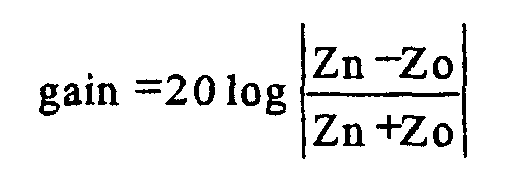
- the reflection gain (in decibels dB) of the circuit 1 as seen looking toward the gate terminal 6 g is given by: where Zo is the antenna impedance (or in the case where no antenna is present, it is the system impedance) and Zn is the input impedance presented by the FET 6 (that is the negative impedance looking towards the gate 6 g ).
- the system/antenna impedance is nominally 50 ohms and the value of the negative impedance is switchable between -45 and -55.555 ohms for I ds1 and I ds2 respectively to give a reflection gain in each case of 25dB. It is to be noted that for these impedance values whilst the reflection gain is constant, the phase of the reflected and amplified signals will be altered by 180 degrees. This change of phase is indicated by the change of the sign of the term (Zn-Zo) ⁇ (Zn + Zo).
- I ds1 is selected such that the FET 6 operates as a negative impedance of -45 ohms and I ds2 is selected such that the FET 6 operates as negative impedance of -55.555 ohms.
- the circuit 2 acts as a binary phase shift key reflective modulator.
- a particular advantage of the modulator circuit 2 is that it provides a simple method of generating BPSK and offers the additional benefit that it also amplifies the signal which it is modulating. Due to the circuit's simplicity it is ideally suited to tagging applications where it further has the advantage that it is capable of operating at very low currents (of the order of a few micro-amps) for an operating frequency of 2.4GHz.
- both the magnitude and phase of the reflected signal can be varied between the two states, such that a combination of amplitude modulation (AM) and phase modulation (PM) can be applied.
- AM amplitude modulation
- PM phase modulation
- the radiated signal 20 can be arranged to be a substantially single sideband signal.
- FIG. 2 there is shown a schematic of a de-spreader circuit 21 for use in a spread spectrum communication system such as for example of the type used in a global positioning system.
- a carrier signal is modulated with a digital code, most often a pseudo random binary sequence (PRBS), to spread its energy spectra.
- PRBS pseudo random binary sequence
- the modulation used is BPSK.
- the circuit 21 is intended for de-spreading such spread spectrum radiation to recover the original carrier signal and any modulation applied thereto. This is achieved by using the modulator 2 of Figure 1 to apply a replica of the sequence used to generate the spread spectrum. It will be appreciated that the sequence applied by the circuit 21 is additionally in time synchronisation with the generating sequence.
- the circuit 21 comprises; an antenna 22 for receiving broad band spread spectrum radiation 23, a broad pass-band filter 24, a narrow stop-band filter 25, a narrow pass-band filter 26 and a modulator circuit 2.
- the broad pass-band filter 24, narrow stop-band filter 25 and narrow pass-band filter 26 are connected in series and the output 28 of the narrow pass-band filter 26 provides the output 28 of the circuit 21.
- the antenna 22 is connected to the input 30 of the broad band filter 24.
- the modulator circuit 2 which is identical to the circuit shown in Figure 1, is connected to the interconnection 32 of the filters 25 and 26.
- the reflective modulator circuit 2 has a gain of 20dB in both reflecting states.
- the reflecting state of the modulator 2 is controlled by a digital signal 34, which as described above is a replica of the original sequence signal used to generate the broad band signal 23. Most typically the signal 34 is a PRBS signal.
- the broad band spread radiation 23 is received and converted to an electrical signal by the antenna 22 and passes through the broad pass-band filter 24 and narrow stop-band filter 25.
- the pass-band of the filter 24 defines the bandwidth of operation of the circuit 21.
- the centre frequency of the stop-band filter 25 is selected to correspond with the carrier frequency of the radiation 23 to block any components at the carrier frequency.
- the filtered signal appearing at the output 32a of the filter 25 is applied to both the input 32b of the narrow pass-band filter 26 and to the input 32c of the modulator 2. Due to the pass-band pass characteristic of the narrow band-pass filter 26 the filtered signal is blocked by the filter 26.
- the filtered signal however appearing at the input 32c of the modulator circuit 2 is de-modulated to produce an amplified version of the original carrier signal which is reflected back to the interconnection 32.
- the amplified carrier signal which is within the band pass characteristic of the narrow pass-band filter 26, passes through substantially unattenuated to the output 28.
- the demodulated signal is prevented from returning to the antenna 22 by the stop-band filter 25.
- the circuit 20 thus operates as a de-spreader circuit and is capable of operating at substantially lower currents than those which currently use digital techniques.
- FIG. 3 is a schematic of a spread spectrum communication system 40 for use in covert communications between a transmitter 42 and a hand held radio receiver 44.
- Spread spectrum communication system 40 for use in covert communications between a transmitter 42 and a hand held radio receiver 44.
- the communication system 40 comprises: a spread spectrum transmitter 42 of a known type which generates a BPSK modulated broad band spread spectrum radiation 46, a reflective de-spreading circuit 48 and a hand held radio receiver 44.
- the de-spreader circuit 48 is identical to the transponder circuit 1 of Figure 1 in which the control circuit 16 switches the transistor 6 using an identical code to that used by the transmitter 42 to generate the spread signal 46.
- the de-spreader circuit 48 thus receives the broad band radiation 46 and in response radiates an amplified and despread narrow band radiation 50 which represents the recovered carrier of the signal 46 and any modulation applied thereto.
- the narrow band radiation 50 is detected by the hand held radio receiver 44.
- the de-spreading circuit 48 is preferably mounted at a high point such as on the side of a building 52 or other structure such as a post or a tree. Since the radiation 46 generated by the transmitter 42 is broad band this makes it difficult for a direction finding receiver to locate the position of the transmitter 42. Although such a direction finding receiver may be able to locate the narrow band radiated emissions 50 from the de-spreading circuit 48 and hence determine its position, it will still be unable to determine the position of the transmitter 42. In a preferred communication system a number of de-spreading circuits 48 (a second such circuit 48a is shown in Figure 3), each having a different modulation code, are located at different physical locations.
- the transmitter 42 is operable to switch between the different modulating codes during communication with the hand held radio 44 such that different de-spreading circuits 48 become activated.
- different de-spreading circuits 48 become activated.
- the position from which the narrow band radiation 50, 50a originates will jump from de-spreading circuit 48 to de-spreading circuit 48a, thereby hampering any attempt to locate the position of the de-spreading circuit.
- the modulator circuit uses a field effect transistor, which is much preferred for operation of microwave frequencies
- the negative impedance amplifier can be implemented in different ways, depending upon the required frequency of operation, such as for example using a bi-polar transistor or other active devices.
- the modulator circuit of the invention is not restricted to the applications described and is suited for use in any application which requires BPSK modulation.
- the present invention resides in the realisation that binary phase shift key modulation can be achieved by using a reflection amplifier and switching the circuit between two reflecting states which preferably have the same reflection gain (though this is not essential when single sideband operation is required), but which change the phase of the reflected signal by substantially 180 degrees.
Landscapes
- Engineering & Computer Science (AREA)
- Computer Networks & Wireless Communication (AREA)
- Signal Processing (AREA)
- Amplitude Modulation (AREA)
- Transmitters (AREA)
- Amplifiers (AREA)
- Digital Transmission Methods That Use Modulated Carrier Waves (AREA)
- Optical Modulation, Optical Deflection, Nonlinear Optics, Optical Demodulation, Optical Logic Elements (AREA)
- Stabilization Of Oscillater, Synchronisation, Frequency Synthesizers (AREA)
- Networks Using Active Elements (AREA)
Abstract
Description
Claims (10)
- A modulator circuit (2)comprising: a negative impedance amplifier (6) operable such that a signal applied to the amplifier is reflected and amplified and switching means (14, 16) for switching the impedance of the amplifier(6) between two reflecting states, the impedances in the two reflecting states being selected such that the phase of the reflected and amplified signal switches by substantially 180 degrees.
- A modulator circuit according to Claim 1 in which the impedances in the two reflecting states are selected such that the reflection gain of the amplifier (6) in the two reflecting states is substantially the same such that the reflected and amplified signal is a binary phase shift keyed.
- A modulator circuit according to Claim in which the impedances in the two reflecting states are selected such that the reflection gain of the amplifier (6) in the two reflecting states is different and wherein said impedances are selected such the reflected and amplified signal is a substantially single sideband signal.
- A modulator circuit according to Claim 1 or Claim 2 in which the negative impedance amplifier comprises a transistor (6) and biasing means (10, 12, 14) for biasing the transistor such as to act as negative impedance amplifier.
- A modulator circuit according to Claim 4 in which the switching means (14, 16) switches the biasing of the transistor (6) to switch the transistor between the two reflecting states.
- A modulator circuit according to any preceding claim and further comprising an antenna (4) for receiving radiation (19) and converting it to the signal applied to the amplifier (6) and for radiating (20) the reflected and amplified signal.
- A modulator circuit according to any one of Claims 4, 5 or 6 in which the transistor (6) comprises a bipolar transistor.
- A modulator circuit according to any one of Claims 4, 5 or 6 in which the transistor (6) comprises a field effect transistor.
- A de-modulator circuit (21) for de-modulating a Binary Phase Shift Keyed signal incorporating a modulator circuit (2) according to any preceding claim.
- A transponder tag incorporating a modulator circuit according to any preceding claim.
Applications Claiming Priority (3)
| Application Number | Priority Date | Filing Date | Title |
|---|---|---|---|
| GB9914941A GB2351423A (en) | 1999-06-25 | 1999-06-25 | Modulator circuit |
| GB9914941 | 1999-06-25 | ||
| PCT/GB2000/002200 WO2001001649A1 (en) | 1999-06-25 | 2000-06-07 | Reflecting modulator circuit comprising a negative impedance amplifier |
Publications (2)
| Publication Number | Publication Date |
|---|---|
| EP1192776A1 EP1192776A1 (en) | 2002-04-03 |
| EP1192776B1 true EP1192776B1 (en) | 2003-10-08 |
Family
ID=10856110
Family Applications (1)
| Application Number | Title | Priority Date | Filing Date |
|---|---|---|---|
| EP00937062A Expired - Lifetime EP1192776B1 (en) | 1999-06-25 | 2000-06-07 | Reflecting modulator circuit comprising a negative impedance amplifier |
Country Status (13)
| Country | Link |
|---|---|
| US (2) | US7046957B1 (en) |
| EP (1) | EP1192776B1 (en) |
| JP (1) | JP4486771B2 (en) |
| KR (1) | KR100667435B1 (en) |
| CN (1) | CN1371566A (en) |
| AT (1) | ATE251826T1 (en) |
| AU (1) | AU5235400A (en) |
| CA (1) | CA2377632A1 (en) |
| DE (1) | DE60005833T2 (en) |
| DK (1) | DK1192776T3 (en) |
| ES (1) | ES2204619T3 (en) |
| GB (1) | GB2351423A (en) |
| WO (1) | WO2001001649A1 (en) |
Families Citing this family (18)
| Publication number | Priority date | Publication date | Assignee | Title |
|---|---|---|---|---|
| GB2351423A (en) * | 1999-06-25 | 2000-12-27 | Marconi Electronic Syst Ltd | Modulator circuit |
| AU2003237866A1 (en) * | 2002-01-22 | 2003-09-02 | Bae Systems Information And Electronic Systems Integration Inc. | Digital rf tag |
| GB2399921B (en) * | 2003-03-26 | 2005-12-28 | Schlumberger Holdings | Borehole telemetry system |
| US8170079B2 (en) * | 2003-07-28 | 2012-05-01 | Los Alamos National Security, Llc | Code division multiple access signaling for modulated reflector technology |
| GB0413112D0 (en) | 2004-06-14 | 2004-07-14 | Texas Instruments Ltd | High bandwidth, high gain receiver equaliser |
| JP2006041952A (en) * | 2004-07-27 | 2006-02-09 | Sony Corp | Information processing apparatus, information device, and control method of information device |
| US7348893B2 (en) | 2004-12-22 | 2008-03-25 | Schlumberger Technology Corporation | Borehole communication and measurement system |
| WO2007044653A1 (en) * | 2005-10-07 | 2007-04-19 | Superconductor Technologies, Inc. | System and method for detecting radio circuits using intermodulation distortion |
| US7768407B2 (en) * | 2007-06-22 | 2010-08-03 | Avery Dennison Corporation | Foldable RFID device interposer and method |
| US7880614B2 (en) * | 2007-09-26 | 2011-02-01 | Avery Dennison Corporation | RFID interposer with impedance matching |
| US8633821B2 (en) * | 2007-12-03 | 2014-01-21 | Avery Dennison Corporation | Dual use RFID/EAS device |
| US8847764B2 (en) * | 2007-12-05 | 2014-09-30 | Avery Dennison Corporation | RFID system with distributed read structure |
| US7786868B2 (en) * | 2007-12-11 | 2010-08-31 | Avery Dennison Corporation | RFID device with multiple passive operation modes |
| ES2659879T3 (en) * | 2010-10-05 | 2018-03-19 | Kapsch Trafficcom Ab | A single antenna vehicle transponder |
| US9184957B2 (en) | 2012-12-27 | 2015-11-10 | Intel Corporation | High speed receivers circuits and methods |
| WO2016011421A1 (en) * | 2014-07-17 | 2016-01-21 | The Regents Of The University Of California | Microwave reflector link, and cdma-spread spectrum reflector apparatus for reduction of unmodulated ambient blockers in reflected data links |
| CN113794454B (en) * | 2021-08-11 | 2023-07-04 | 西安电子科技大学 | Single-ended input reflection amplifier circuit based on cross-coupling negative resistance circuit |
| CN113794451B (en) * | 2021-08-11 | 2023-06-30 | 西安电子科技大学 | Low-power consumption single-ended reflection amplifier circuit based on oscillation negative resistance characteristic |
Family Cites Families (19)
| Publication number | Priority date | Publication date | Assignee | Title |
|---|---|---|---|---|
| DE1912852C3 (en) | 1969-03-13 | 1978-05-11 | Siemens Ag, 1000 Berlin Und 8000 Muenchen | Reflection amplifier for very short electromagnetic waves |
| US4075632A (en) * | 1974-08-27 | 1978-02-21 | The United States Of America As Represented By The United States Department Of Energy | Interrogation, and detection system |
| JPS57111158A (en) * | 1980-12-26 | 1982-07-10 | Fujitsu Ltd | Reflective phase modulator |
| JPS60104945A (en) * | 1983-11-14 | 1985-06-10 | Konishiroku Photo Ind Co Ltd | Automatic developing machine |
| JPS61257050A (en) * | 1985-05-10 | 1986-11-14 | Hitachi Shonan Denshi Kk | Psk modulation circuit |
| JPS63198452A (en) * | 1987-02-13 | 1988-08-17 | Matsushita Electric Works Ltd | Reflection type phase modulator |
| JPS63262906A (en) | 1987-04-20 | 1988-10-31 | Sharp Corp | Ssb modulator |
| CA1335676C (en) * | 1988-01-14 | 1995-05-23 | Akira Iga | Portable data transmitter device and a system using the same |
| FR2650905B1 (en) * | 1989-08-08 | 1994-08-26 | Guena Jean | RADIO SYSTEM FOR TRANSMITTING DATA TO A LOW COST PASSIVE END |
| JPH03113387A (en) * | 1989-09-27 | 1991-05-14 | Nippon Soken Inc | Transponder for moving body identifying device |
| JPH0496520A (en) * | 1990-08-13 | 1992-03-27 | Sharp Corp | Data transmitter |
| FR2669475B1 (en) * | 1990-11-16 | 1993-01-22 | Thomson Composants Microondes | MODEM FOR MICROWAVE BADGE WITH REFLECTION AMPLIFIER. |
| FR2669484B1 (en) * | 1990-11-16 | 1994-03-25 | Thomson Composants Microondes | ELECTROMAGNETIC WAVE TELECOMMUNICATIONS DEVICE. |
| JPH06104945A (en) | 1992-09-22 | 1994-04-15 | Hitachi Chem Co Ltd | Two-phase modulation circuit |
| IL105796A0 (en) * | 1993-05-24 | 1993-10-20 | Tadiran Ltd | Vehicle service utilization monitoring system and equipment and methods useful therewith |
| GB9324534D0 (en) * | 1993-11-30 | 1994-01-19 | Marconi Gec Ltd | Circuit arrangement |
| US5649295A (en) * | 1995-06-19 | 1997-07-15 | Lucent Technologies Inc. | Dual mode modulated backscatter system |
| GB9616610D0 (en) * | 1996-08-08 | 1996-09-25 | Marconi Gec Ltd | Interrogator circuit arrangement |
| GB2351423A (en) * | 1999-06-25 | 2000-12-27 | Marconi Electronic Syst Ltd | Modulator circuit |
-
1999
- 1999-06-25 GB GB9914941A patent/GB2351423A/en not_active Withdrawn
-
2000
- 2000-06-07 CN CN00812022A patent/CN1371566A/en active Pending
- 2000-06-07 WO PCT/GB2000/002200 patent/WO2001001649A1/en not_active Ceased
- 2000-06-07 AT AT00937062T patent/ATE251826T1/en not_active IP Right Cessation
- 2000-06-07 US US10/019,140 patent/US7046957B1/en not_active Expired - Lifetime
- 2000-06-07 ES ES00937062T patent/ES2204619T3/en not_active Expired - Lifetime
- 2000-06-07 EP EP00937062A patent/EP1192776B1/en not_active Expired - Lifetime
- 2000-06-07 KR KR1020017016364A patent/KR100667435B1/en not_active Expired - Lifetime
- 2000-06-07 DK DK00937062T patent/DK1192776T3/en active
- 2000-06-07 CA CA002377632A patent/CA2377632A1/en not_active Abandoned
- 2000-06-07 AU AU52354/00A patent/AU5235400A/en not_active Abandoned
- 2000-06-07 JP JP2001506203A patent/JP4486771B2/en not_active Expired - Lifetime
- 2000-06-07 DE DE60005833T patent/DE60005833T2/en not_active Expired - Lifetime
-
2006
- 2006-05-15 US US11/434,571 patent/US7551903B2/en not_active Expired - Fee Related
Also Published As
| Publication number | Publication date |
|---|---|
| US7046957B1 (en) | 2006-05-16 |
| ATE251826T1 (en) | 2003-10-15 |
| US7551903B2 (en) | 2009-06-23 |
| WO2001001649A1 (en) | 2001-01-04 |
| CA2377632A1 (en) | 2001-01-04 |
| GB9914941D0 (en) | 2000-05-24 |
| JP4486771B2 (en) | 2010-06-23 |
| GB2351423A (en) | 2000-12-27 |
| DE60005833T2 (en) | 2004-05-06 |
| AU5235400A (en) | 2001-01-31 |
| KR20020029336A (en) | 2002-04-18 |
| KR100667435B1 (en) | 2007-01-10 |
| DK1192776T3 (en) | 2003-11-03 |
| ES2204619T3 (en) | 2004-05-01 |
| DE60005833D1 (en) | 2003-11-13 |
| EP1192776A1 (en) | 2002-04-03 |
| JP2003503903A (en) | 2003-01-28 |
| CN1371566A (en) | 2002-09-25 |
| US20060279370A1 (en) | 2006-12-14 |
Similar Documents
| Publication | Publication Date | Title |
|---|---|---|
| US7046957B1 (en) | Reflecting modulator circuit comprising a negative impedance amplifier | |
| US4979186A (en) | Time domain radio transmission system | |
| GB2234141A (en) | Microwave responder has microstrip lines separated by diode | |
| WO1990010980A1 (en) | Time domain radio transmission system | |
| CN1307686A (en) | Reflector circuit | |
| FR2669475A1 (en) | MODEM FOR HYPERFREQUENCY BADGE, WITH REFLECTIVE AMPLIFIER. | |
| US6176432B1 (en) | Modulating and demodulating device | |
| EP0486364B1 (en) | Data-exchange system using electromagnetic waves | |
| JP2947425B2 (en) | Active antenna for two-way communication | |
| AU706255B2 (en) | Tag | |
| US4647930A (en) | Passive radar responder | |
| CA2055581A1 (en) | Electromagnetic wave telecommunication device | |
| JP2002505041A (en) | Vehicle equipment for transponder operation | |
| US7804454B1 (en) | Active high frequency transmitter antenna assembly | |
| US7065328B1 (en) | Superregenerative AM demodulator | |
| Bracht et al. | Using an impedance-modulated reflector for passive communication | |
| US12316034B2 (en) | Antenna array for passively modulating radio frequency signals | |
| JPS6128229A (en) | Radar reflector having two-way communication function | |
| JPH0998106A (en) | Microwave radio | |
| JPH02218986A (en) | Transponder for mobile object identification |
Legal Events
| Date | Code | Title | Description |
|---|---|---|---|
| PUAI | Public reference made under article 153(3) epc to a published international application that has entered the european phase |
Free format text: ORIGINAL CODE: 0009012 |
|
| 17P | Request for examination filed |
Effective date: 20020119 |
|
| AK | Designated contracting states |
Kind code of ref document: A1 Designated state(s): AT BE CH CY DE DK ES FI FR GB GR IE IT LI LU MC NL PT SE |
|
| AX | Request for extension of the european patent |
Free format text: AL;LT;LV;MK;RO;SI |
|
| GRAH | Despatch of communication of intention to grant a patent |
Free format text: ORIGINAL CODE: EPIDOS IGRA |
|
| RAP1 | Party data changed (applicant data changed or rights of an application transferred) |
Owner name: A.B. DICK HOLDINGS LIMITED |
|
| GRAH | Despatch of communication of intention to grant a patent |
Free format text: ORIGINAL CODE: EPIDOS IGRA |
|
| GRAA | (expected) grant |
Free format text: ORIGINAL CODE: 0009210 |
|
| RAP1 | Party data changed (applicant data changed or rights of an application transferred) |
Owner name: MARCONI UK INTELLECTUAL PROPERTY LTD |
|
| AK | Designated contracting states |
Kind code of ref document: B1 Designated state(s): AT BE CH CY DE DK ES FI FR GB GR IE IT LI LU MC NL PT SE |
|
| PG25 | Lapsed in a contracting state [announced via postgrant information from national office to epo] |
Ref country code: LI Free format text: LAPSE BECAUSE OF FAILURE TO SUBMIT A TRANSLATION OF THE DESCRIPTION OR TO PAY THE FEE WITHIN THE PRESCRIBED TIME-LIMIT Effective date: 20031008 Ref country code: BE Free format text: LAPSE BECAUSE OF FAILURE TO SUBMIT A TRANSLATION OF THE DESCRIPTION OR TO PAY THE FEE WITHIN THE PRESCRIBED TIME-LIMIT Effective date: 20031008 Ref country code: NL Free format text: LAPSE BECAUSE OF FAILURE TO SUBMIT A TRANSLATION OF THE DESCRIPTION OR TO PAY THE FEE WITHIN THE PRESCRIBED TIME-LIMIT Effective date: 20031008 Ref country code: CH Free format text: LAPSE BECAUSE OF FAILURE TO SUBMIT A TRANSLATION OF THE DESCRIPTION OR TO PAY THE FEE WITHIN THE PRESCRIBED TIME-LIMIT Effective date: 20031008 Ref country code: AT Free format text: LAPSE BECAUSE OF FAILURE TO SUBMIT A TRANSLATION OF THE DESCRIPTION OR TO PAY THE FEE WITHIN THE PRESCRIBED TIME-LIMIT Effective date: 20031008 Ref country code: FI Free format text: LAPSE BECAUSE OF FAILURE TO SUBMIT A TRANSLATION OF THE DESCRIPTION OR TO PAY THE FEE WITHIN THE PRESCRIBED TIME-LIMIT Effective date: 20031008 Ref country code: CY Free format text: LAPSE BECAUSE OF FAILURE TO SUBMIT A TRANSLATION OF THE DESCRIPTION OR TO PAY THE FEE WITHIN THE PRESCRIBED TIME-LIMIT Effective date: 20031008 |
|
| REG | Reference to a national code |
Ref country code: GB Ref legal event code: FG4D |
|
| REG | Reference to a national code |
Ref country code: CH Ref legal event code: EP |
|
| REG | Reference to a national code |
Ref country code: DK Ref legal event code: T3 |
|
| REG | Reference to a national code |
Ref country code: IE Ref legal event code: FG4D |
|
| REF | Corresponds to: |
Ref document number: 60005833 Country of ref document: DE Date of ref document: 20031113 Kind code of ref document: P |
|
| PG25 | Lapsed in a contracting state [announced via postgrant information from national office to epo] |
Ref country code: GR Free format text: LAPSE BECAUSE OF FAILURE TO SUBMIT A TRANSLATION OF THE DESCRIPTION OR TO PAY THE FEE WITHIN THE PRESCRIBED TIME-LIMIT Effective date: 20040108 Ref country code: SE Free format text: LAPSE BECAUSE OF FAILURE TO SUBMIT A TRANSLATION OF THE DESCRIPTION OR TO PAY THE FEE WITHIN THE PRESCRIBED TIME-LIMIT Effective date: 20040108 |
|
| NLV1 | Nl: lapsed or annulled due to failure to fulfill the requirements of art. 29p and 29m of the patents act | ||
| LTIE | Lt: invalidation of european patent or patent extension |
Effective date: 20031008 |
|
| REG | Reference to a national code |
Ref country code: CH Ref legal event code: PL |
|
| ET | Fr: translation filed | ||
| REG | Reference to a national code |
Ref country code: ES Ref legal event code: FG2A Ref document number: 2204619 Country of ref document: ES Kind code of ref document: T3 |
|
| PG25 | Lapsed in a contracting state [announced via postgrant information from national office to epo] |
Ref country code: IE Free format text: LAPSE BECAUSE OF NON-PAYMENT OF DUE FEES Effective date: 20040607 Ref country code: LU Free format text: LAPSE BECAUSE OF NON-PAYMENT OF DUE FEES Effective date: 20040607 |
|
| PG25 | Lapsed in a contracting state [announced via postgrant information from national office to epo] |
Ref country code: MC Free format text: LAPSE BECAUSE OF NON-PAYMENT OF DUE FEES Effective date: 20040630 Ref country code: DK Free format text: LAPSE BECAUSE OF NON-PAYMENT OF DUE FEES Effective date: 20040630 |
|
| PLBE | No opposition filed within time limit |
Free format text: ORIGINAL CODE: 0009261 |
|
| STAA | Information on the status of an ep patent application or granted ep patent |
Free format text: STATUS: NO OPPOSITION FILED WITHIN TIME LIMIT |
|
| 26N | No opposition filed |
Effective date: 20040709 |
|
| REG | Reference to a national code |
Ref country code: DK Ref legal event code: EBP |
|
| REG | Reference to a national code |
Ref country code: IE Ref legal event code: MM4A |
|
| REG | Reference to a national code |
Ref country code: GB Ref legal event code: 732E |
|
| PG25 | Lapsed in a contracting state [announced via postgrant information from national office to epo] |
Ref country code: IT Free format text: LAPSE BECAUSE OF NON-PAYMENT OF DUE FEES;WARNING: LAPSES OF ITALIAN PATENTS WITH EFFECTIVE DATE BEFORE 2007 MAY HAVE OCCURRED AT ANY TIME BEFORE 2007. THE CORRECT EFFECTIVE DATE MAY BE DIFFERENT FROM THE ONE RECORDED. Effective date: 20050607 |
|
| PGFP | Annual fee paid to national office [announced via postgrant information from national office to epo] |
Ref country code: ES Payment date: 20050607 Year of fee payment: 6 |
|
| REG | Reference to a national code |
Ref country code: FR Ref legal event code: TP |
|
| PG25 | Lapsed in a contracting state [announced via postgrant information from national office to epo] |
Ref country code: ES Free format text: LAPSE BECAUSE OF NON-PAYMENT OF DUE FEES Effective date: 20060608 |
|
| REG | Reference to a national code |
Ref country code: ES Ref legal event code: FD2A Effective date: 20060608 |
|
| PG25 | Lapsed in a contracting state [announced via postgrant information from national office to epo] |
Ref country code: PT Free format text: LAPSE BECAUSE OF NON-PAYMENT OF DUE FEES Effective date: 20040308 |
|
| REG | Reference to a national code |
Ref country code: FR Ref legal event code: PLFP Year of fee payment: 17 |
|
| REG | Reference to a national code |
Ref country code: FR Ref legal event code: PLFP Year of fee payment: 18 |
|
| REG | Reference to a national code |
Ref country code: FR Ref legal event code: PLFP Year of fee payment: 19 |
|
| PGFP | Annual fee paid to national office [announced via postgrant information from national office to epo] |
Ref country code: DE Payment date: 20190515 Year of fee payment: 20 |
|
| PGFP | Annual fee paid to national office [announced via postgrant information from national office to epo] |
Ref country code: FR Payment date: 20190522 Year of fee payment: 20 |
|
| PGFP | Annual fee paid to national office [announced via postgrant information from national office to epo] |
Ref country code: GB Payment date: 20190524 Year of fee payment: 20 |
|
| REG | Reference to a national code |
Ref country code: DE Ref legal event code: R071 Ref document number: 60005833 Country of ref document: DE |
|
| REG | Reference to a national code |
Ref country code: GB Ref legal event code: PE20 Expiry date: 20200606 |
|
| PG25 | Lapsed in a contracting state [announced via postgrant information from national office to epo] |
Ref country code: GB Free format text: LAPSE BECAUSE OF EXPIRATION OF PROTECTION Effective date: 20200606 |