EP1191331A2 - Method for manufacturing tips and probes for a STM or an AFM - Google Patents
Method for manufacturing tips and probes for a STM or an AFM Download PDFInfo
- Publication number
- EP1191331A2 EP1191331A2 EP01870192A EP01870192A EP1191331A2 EP 1191331 A2 EP1191331 A2 EP 1191331A2 EP 01870192 A EP01870192 A EP 01870192A EP 01870192 A EP01870192 A EP 01870192A EP 1191331 A2 EP1191331 A2 EP 1191331A2
- Authority
- EP
- European Patent Office
- Prior art keywords
- layer
- probe tip
- probe
- recited
- etching
- Prior art date
- Legal status (The legal status is an assumption and is not a legal conclusion. Google has not performed a legal analysis and makes no representation as to the accuracy of the status listed.)
- Granted
Links
Images






Classifications
-
- G—PHYSICS
- G01—MEASURING; TESTING
- G01Q—SCANNING-PROBE TECHNIQUES OR APPARATUS; APPLICATIONS OF SCANNING-PROBE TECHNIQUES, e.g. SCANNING PROBE MICROSCOPY [SPM]
- G01Q70/00—General aspects of SPM probes, their manufacture or their related instrumentation, insofar as they are not specially adapted to a single SPM technique covered by group G01Q60/00
- G01Q70/16—Probe manufacture
-
- G—PHYSICS
- G01—MEASURING; TESTING
- G01Q—SCANNING-PROBE TECHNIQUES OR APPARATUS; APPLICATIONS OF SCANNING-PROBE TECHNIQUES, e.g. SCANNING PROBE MICROSCOPY [SPM]
- G01Q70/00—General aspects of SPM probes, their manufacture or their related instrumentation, insofar as they are not specially adapted to a single SPM technique covered by group G01Q60/00
- G01Q70/06—Probe tip arrays
Definitions
- the present invention is generally related to a scanning tunnelling or atomic force microscope and more particularly to the manufacturing of tip and probe used in said scanning tunnelling or atomic force microscope.
- Scanning tunnelling microscopy (STM) and electrical atomic force microscopy (AFM) enables us today to carry out electrical and/or topographical measurements on modern semiconductor devices with nanometer (nm) spatial resolution. These measurements are done by scanning at least one small conductive tip over the device surface and recording at the same time topographical information and/or electrical signals.
- Metal is preferably used as tip material due to its excellent electrical conductivity.
- Silicon (Si) tips with a thin metal coating, typically 10-25 nm thick, are commercially available since the early 1990's but the metal coatings rapidly wear off. Therefore solid metal pyramids made by the so-called moulding technique have been developed which are integrated into Si cantilevers or metal cantilevers.
- the metal cantilever probes, also called full metal probes, are preferred because they are highly conductive and require fewer process steps.
- European Patent No 0899538 A probe tip configuration, a method of fabricating probe tips and use thereof", (which is hereby incorporated by reference in its entirety) the inventors discloses a method of fabricating probe tips applying said so-called moulding technique.
- European Patent No. 0763844 entitled "method of manufacturing micro-tip and female mould substrate therefor, and method of manufacturing probe with micro-tip” (which is hereby incorporated by reference in its entirety) some of these disadvantages are indicated.
- the inventor T. Yagi proposes a method to overcome some of the above-mentioned disadvantages, as illustrated in figure 2.
- the first substrate is used to define the probe tip (23) while the second substrate is used to define the cantilever.
- the first substrate could be re-used.
- This method only comprises front side processing steps and avoids the backside lithography and time consuming etching steps required to create a probe membrane or to release the probe membrane.
- This method requires only one substrate to form a fully probe consisting of probe tip, cantilever and probe membrane. This method allows easy removal of the probe prior to mounting the probe into a scanning microscope.
- Another aim of the present invention is to disclose a method for manufacturing a full metal probe only comprising front side lithography steps, allowing the probe tip and the cantilever to be separately processed.
- the probe tip can be made from a material or metallisation scheme different from that of the cantilever.
- the characteristics of the probe tip can optimised independently from the cantilever.
- This method only comprises front side processing steps and avoids the backside lithography and time consuming etching steps required to create a probe membrane or to release the probe membrane.
- One object of the invention is to present a method comprising the steps of providing a substrate, depositing on said substrate a hard mask.
- a mould is created in said hard mask and said substrate.
- a first layer is deposited on said patterned hard mask.
- This first layer has a sufficiently high enough adhesion to said hard mask to allow further processing, but this adhesion force is weak enough to be overcome when peeling the probe gradually from said underlying hard mask.
- said first layer is patterned to form a probe tip configuration comprising at least a probe tip. By partially or fully under-etching said probe tip configuration from the front side of the substrate, the probe tip configuration can be removed from said substrate by lifting the probe.
- Said method can further comprise the step of forming selective to said patterned first layer at least one additional layer before under-etching said patterned stack.
- Said method can further comprise the step of mounting a holder chip to said probe tip configuration before peeling of the probe.
- Said hard mask can be nitride, oxide, oxynitride or a combination of layers.
- Said first layer can be a metal, preferably a stack of Ti:W and Au.
- Another object of the invention is to present a method for manufacturing a full metal probe only comprising front side lithography and processing steps, allowing the probe tip and the cantilever to be separately processed.
- the probe tip can be made from a material or metallisation scheme different from the cantilever.
- the area of the probe tip is defined in an intermediate, third, patterning step.
- a second layer can be deposited on said hard mask and said patterned first layer. This second layer will be patterned in the last patterning step to define the probe tip configuration consisting of probe membrane or contact area, cantilever and overlapping the probe tip area.
- Said second layer can be a metal, preferably a stack of Ti:W and Au.
- Said method can further comprise the step of forming selective to said patterned second layer at least one additional layer before under-etching said patterned stack.
- Figure 1 represents a prior art method of manufacturing a full metal probe comprising a tip, cantilever and membrane applying the moulding technique, illustrated by cross sectional views
- Figure 2 represents a prior art method of manufacturing a tip to avoid backside etching of the moulding substrate, illustrated by cross sectional views
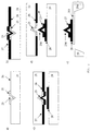
- Figure 3 represents a process scheme for peel-off probes made by two lithography steps, upper part is top view, and bottom part is a cross sectional view along section AA.
- Figure 4 represents a probe with 4 cantilevers illustrating the peel-off process illustrating the options of fully or partially under-etching the probe
- Figure 5 represents a probe removal by peel-off according to an embodiment of the present invention
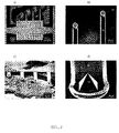
- Figure 6 represents a SEM picture of full metal peel off probe according to the preferred embodiment
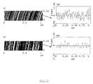
- Figure 7 represents a topography measurements done on a SrTiO3 calibration sample in tapping mode. Left side shows the AFM picture. Right side shows the measured height h measured along the cross section x.
- Figure 8 represents a process scheme for peel-off probes with different metallization scheme for probe tip and cantilever, upper part is top view, and bottom part is a cross sectional view along section AA
- Figure 9 represents a metal cantilever with hardened tip made by peel off according to one embodiment of the invention.
- Figure 10 represents I-V measurements in point contact mode using an unhardened Ni tip (a) or a hardened Ni tip (b) according to an embodiment of the invention
- Figure 11 represents a comparison of unhardened Ni pyramidal tip (a) and hardened Ni pyramidal tip (b), diamond pyramidal tip (c) according to an embodiment of the invention using SSRM on InP(S) substrate comprising an npn structure.
- a method for manufacturing probes only applying front side processing steps, more precisely lithographic steps, is disclosed.
- the method allows an easy removal of the probe tip by peeling off the manufactured probe from the underlying substrate.
- a method for manufacturing a scanning probe requiring only front side processing steps comprises only two front side lithographic steps.
- the peel-off effect is achieved by selectively metallising the area of the probe tip configuration.
- This metal layer has a sufficiently high enough adhesion to the substrate to allow further processing, but this adhesion force is weak enough to be overcome when peeling the probe gradually from the wafer.
- a mould (34) is formed in the starting substrate (31), preferably a silicon wafer.
- This mould can have various forms: pyramidal, a truncated cone, a cylinder.
- a truncated pyramidal etch pit is formed by anisotropically etching the substrate trough an opening defined in a masking layer formed on top of the substrate.
- a masking layer can be a photo resist or a hard mask (32), e.g. nitride, oxide, oxynitride or a combination of layers.
- This step of defining the probe tip configuration comprises the first front side lithographic step.
- the probe tip configuration is defined (fig 3c).
- the probe tip configuration consists at least of the probe tip (34), but can also comprise the cantilever (41) and/or the contact area (37) in case a complete probe has to be manufactured.
- additional layers (35) can be deposited using techniques known to a person skilled in the art. If the first layer is a metal additional layers can be plated onto this first layer to create a stack having the desired properties. Such properties are e.g. the mechanical strength of the cantilever that may require a certain thickness, wear-out properties of the probe tip that may require a certain stack composition and hence puts also requirements on the first layer.
- Further processing can comprise wet processing steps such as plating, wet etching, cleaning or temperature processing steps such as annealing steps.
- the probe tip configuration is fully or partially under-etched (36) (fig 3d) from the front side of the substrate.
- a hard mask is used, first the hard mask is removed using the probe tip configuration as a masking layer. Underneath the area of the probe tip configuration the hard mask remains. Then the substrate is etched from the front side selective to the probe tip configuration. Partially under-etching will only release the probe tip from the substrate. Fully under-etching will also release the cantilever. Preferably this under-etching is done using an isotropic etch chemistry, e.g. a wet etch such as a KOH-mixture in case of silicon substrates.
- the probe can now be peeled off from the substrate (fig 3e)
- a holder chip (53) can be attached to the probe, e.g. to the contact area if formed, to ease further handling or mounting of the probe. If so, a substantial part of the probe tip configuration, comprising the first layer and additional layers formed upon, is temporarily spaced apart from the underlying substrate or hard mask. (fig 5c) The holder chip is attached to the probe (fig 5e) and holder chip with the probe is then fully removed from the first surface (fig 5f).
- the starting substrates (31) were (100) -Si wafers having a diameter of 150 mm. These wafers were covered (32) with 470 nanometer (nm) thermally grown oxide, SiO 2 , and 150nm low-pressure chemical vapour deposited (LPCVD) nitride, Si 3 N 4 .
- Photoresist was spun onto the wafers and squares (34) of 40x40 square micrometer ( ⁇ m 2 ) were opened in the photoresist during the first lithography step. These squares define the tip area (34).
- This resist pattern was then transferred to the Si 3 N 4 layer by reactive ion etching (RIE) using a SF 6 :O 2 etching mixture.
- RIE reactive ion etching
- the resist was removed and the nitride pattern was transferred to the SiO 2 layer by etching the oxide layer with buffered HF (BHF). Inverted pyramids were then etched in 30% KOH at 70°C for 55 minutes. The wafer surface was covered with a 10nm thick layer of sputtered Ti:W followed by a 30 nm thick layer of evaporated Au (33). (see figure 3b)
- Photoresist was again spun onto the wafer.
- the resist outside the area of the probe tip configuration was removed by the second lithography step, thereby leaving the area of the probe tip configuration covered with resist.
- the Au layer was etched in a solution of KI:I 2 :H 2 O.
- the Ti:W layer was removed by RIE in a SF 6 atmosphere.
- the photoresist was stripped.
- a 12 ⁇ m thick Ni layer (35) was deposited on the area of the probe tip configuration by electroless Nickel (Ni) plating. Prior to this plating the wafer was pre-treated in a PdCl 2 solution which helps to initiate the autocatalytic Ni deposition. The plating was done in two steps. First, 1 ⁇ m of Ni was deposited using the MeTeC-NiP-LT bath from OTB Berlin (Berlin, Germany). The bath temperature was 70°C and the deposition time was 10 minutes. This solution showed in all experiments an excellent starting behaviour but the plated Ni films had a rough surface that would prevent the laser light from being reflected to the detector in the AFM. This first layer is therefore used as a starting layer for the next plating step.
- the second plating step was done using the ENPLATE Ni 434E bath from Enthone-OMI ('s-Hertogenbosch, Netherlands) at 85°C for 1 hour until its final value of 12 ⁇ m. Rough Ni surfaces were smoothed after being plated for some time in the Enthone-OMI solution. After plating the wafer was rinsed in a water bath which had the same temperature as the plating bath in order to prevent the formation of mechanical stress in the plated Ni film. Rinsing the wafer in cold water immediately after plating resulted in cracks in the Ni cantilevers and the lift-off of plated structures. It should be mentioned that a fresh Enthone-OMI solution had to be used for each plating run.
- the structures were only partially plated if the same bath was used twice.
- the OTB-Berlin bath showed a good long-term stability and could be used for many runs. (see figure 3c)
- the selective deposition of the thick Ni films was improved by applying this two-step plating process.
- Figure 4 illustrates the under-etching of the cantilevers during the anistropic KOH etching.
- one probe has four cantilevers (41), respectively 200, 400, 600 and 800 ⁇ m long.
- the cantilevers are 65 ⁇ m wide and 12 ⁇ m thick.
- Figure 4a shows the probe before etching with the Si 3 N 4 layer (32) still in place (Fig 4a).
- Figures 4b illustrates the case of under-etching the cantilevers (41), the tips (34) and the bridges (42) (Fig 4b).
- Figure 4c shows the probe after the probe membrane was peeled off (Fig 4c). The yield after under-etching was nearly 100%, which was also confirmed by several process runs.
- FIG. 5 shows the peeling procedure schematically. A cross section of the probe tip configuration before peeling can be seen in Fig 5a. First, one of the two bridges (42, figure 4b) was lifted up with a sharp needle (51) under a microscope (Fig 5b). After the bridge was broken, the probe membrane (35,33) was gradually peeled off (Fig 5c). After removing the needle, the membrane fell back into its initial position (Fig 5d). The connection between the membrane (35,33) and the nitride (32) is no longer present.
- the probe only remains attached to the substrate via the unbroken bridge.
- Silicon chips (53) (3.0 mm long, 1.2 mm wide, 0.6mm thick) metallized with 20 nm Ti:W+45 nm Ni+100 nm Au (52) were then soldered (54) to the probe membranes (35) by a procedure which is described in detail in "Mounting of moulded AFM probes by soldering" , Proc of SPIE 4175, 2000. After soldering, the probe was peeled off completely only using a pair of tweezers (51) (Fig 5f). The whole wafer containing about 600 probes was mounted in this way. By partially peeling off the probe membranes before the soldering step the removal of the probe with holder chip turned out to be very easy and didn't require additional handling.
- Fig 6a shows a peel-off probe after it was removed from the wafer. It can be seen that the metal membrane (33) is fixed to the Si chip (53) by the solder connection (54). The bright area on the probe membrane is metal which indicates the peel-off area. The dark area is Si 3 N 4 from the under-etched area.
- Fig 6b shows the end of a full metal cantilever beam. It can be seen that cantilever (41) and metal pyramid (34) are well defined. A close-up of the tip is shown in Fig 6c. The tips had a radius of typically 50 to 100nm which is slightly higher compared to previous fabricated probes, typically 20 to 50nm. This was due to the long under-etching time of 5 hours where the tip was attacked by the KOH.
- Figure 7 compares topography measurements on a calibration surface, such as SrTiO 3 , with a Si cantilever with integrated metal pyramid and a peel off probe according to the invention.
- the metal pyramid on the Si cantilever is clearly sharper than the one on the peel off probe.
- FIG. 4d A schematic cross-section of figure 4d is drawn underneath the picture. Only during the last minutes of the etching of the tip is exposed to the etching solution. After cutting one bridge (42), the probe was gradually peeled off as described above.
- Figure 4e shows the wafer surface after removal of the probe. So if only the pyramidal tip (34) is under-etched, the probe with hardened probe tip (34), cantilever (41) and contact (37) area can still be peeled off.
- a method for manufacturing a full metal probe is disclosed only comprising front side lithography steps, allowing the probe tip and the cantilever to be separately processed.
- the probe tip can be made from a material or metallisation scheme different from the cantilever.
- the probe tip and cantilever are made of the same material but in a separate and different metallisation scheme.
- the hardness of as-deposited Ni films made by electroless plating can be increased from about 500HV (HV: Hardness Vickers) up to 1000HV by an annealing the Ni-plated probe tip at 300 to 400°C.
- HV Hardness Vickers
- Such methods are for example disclosed in "Nickel and chromium plating", 2 nd edition, J.K. Denis et al., Butterworths ltd, p. 269-277, 1986, which is hereby incorporated by reference.
- the plating step and the subsequent annealing step are to be executed after the processing of the probe tip. After applying this procedure on full metal probes a strong bending of the cantilever was however observed, probably due the thermomechanical stress in the cantilever.
- the step of annealing the Ni probe tips has to be executed before manufacturing the Ni cantilevers.
- This separate processing of probe tips and cantilever was achieved by carrying out two metallization steps.
- the overall fabrication process is similar to that described in another embodiment of this invention and therefore only the main steps are discussed.
- the tip area (34) was metallized by a lift-off procedure. Photoresist was again spun onto the wafer. Applying an additional lithography step will remove the resist substantially above the inverted pyramids. During this additional lithography step the probe tip mask of the first lithography step, used to define the probe tip area (34), is used again. The wafer was then covered with 10nm Ti:W+30nm Au (43). The metal film was structured by lift-off leaving only the probe tip area covered with metal, applying techniques known to a person skilled in the art (see figure 8b).
- the thickness of the metal stack within the area of the probe tip configuration was then increased up to 4 ⁇ m by exposing the wafer to the Ni plating solution from OTB-Berlin at 70°C for 30 minutes as disclosed in another embodiment of the invention (see figure 8c).
- the pyramidal tip is thus at least partially filled.
- some tips were hardened by rapid thermal annealing (RTA) for 10 minutes at 300°C.
- Other tips were annealed at 400°C. Longer anneal times, e.g. 1 hour, can improve the hardness of the probe tip.
- the full wafer surface was then again coated with 10 nm Ti:W+30nm Au (33).
- the area of the probe tip configuration (35) was covered with resist and the stack of Au and Ti:W is etched away outside this area (see figure 8d).
- the two-step Ni plating sequence was again applied to metallize the area of the probe tip configuration, as disclosed in another embodiment.
- the cantilevers (41) were under-etched (see figure 8e) and the probes were peeled off from the wafer.
- Figure 9a shows the probe topside imaged by an optical microscope after the under-etching was completed.
- the Ni surface (35) is very smooth and the separately metallised tip area (34) can be clearly distinguished in Figure 9b.
- the tip area is slightly higher than the cantilever because it was plated twice.
- Figure 9c shows a metal membrane from the tip side imaged by scanning electron microscopy (SEM).
- SEM scanning electron microscopy
- the pyramidal tip shown in the close-up in Figure 9d was annealed at 400°C. The clean side walls indicate that there was no reaction between the Ti:W and the Si during the RTA step.
- the probe tip and cantilever are made of the different materials, each having an appropriated metallization scheme.
- the described procedure can also be used to make the tip from materials different from the cantilever material, applying e.g. Cr or diamond to obtain a harder probe tip.
- the anneal time can depend on the material used and can be further adapted depending on the desired hardness of the probe tip. This does not affect the peeling procedure.
- the separation between the two metallisation schemes is done by applying an additional patterning step to pattern the probe tip material. Subsequent process steps to improve the quality of the probe tip, such as annealing, can be done after this patterning. Additional material deposition can be done afterwards if the deposition process is selective with respect to the patterned probe tip. Otherwise additional patterning steps are required. As no backside etching is performed the probe tip, and later on, also the cantilever are supported by the full silicon wafer.
- Figure 10 -11 illustrate the good electrical and mechanical behaviour of probe tips made according to one or more embodiments of the present invention.
- I-V measurements on n-type Si were done in order to find out if the hardened metal tips are able to establish a stable Ohmic contact on Si. It is well-known that an Ohmic contact on Si can only be obtained by transforming the Si underneath the tip to the so-called metallic ⁇ -tin phase. A pressure of 10-12 GPa is needed for that and the unhardened Ni tips withstood this high pressure only for a very short time as can be seen in figure 10a.
- the first I-V curve (solid line) was collected after increasing the force until the point where the contact behaviour changed from Schottky to Ohmic.
- the second I-V curve (dashed line) was collected shortly afterwards and showed already an increase in resistance indicating rapid tip degradation at high forces.
- Figure 10b shows a set of 20 I-V curves measured using a peel-off probe where the Ni tip was hardened by an annealing step at 400°C for 10 minutes. It can be clearly seen that the hardened probe tip withstands the high forces in point contact and holds the Ohmic regime. The Ohmic regime was also achieved after scanning the tip over the surface for a while and going back into point contact.
- test sample was a multilayer InP structures which was epitaxially grown by metal-organic chemical vapor deposition (MOCVD).
- MOCVD metal-organic chemical vapor deposition
- the layer structure was p-n-p on a semi-insulating InP(S) substrate where the n-type layer was Si doped and the p-type layers were Zn doped.
- SSRM measurements were done on a cleaved cross section using a scan size of 10x10 ⁇ m 2 and a scan speed of 1 Hz.
- the sample was biased at 3.0 V and the same high force was applied to the three probe tips during scanning. No significant difference was found between hardened and unhardened Ni tips.
- the peel off probes performed as good as the Si cantilever probes manufactured according to the prior art technology.
Landscapes
- Physics & Mathematics (AREA)
- Health & Medical Sciences (AREA)
- General Health & Medical Sciences (AREA)
- General Physics & Mathematics (AREA)
- Nuclear Medicine, Radiotherapy & Molecular Imaging (AREA)
- Radiology & Medical Imaging (AREA)
- Measuring Leads Or Probes (AREA)
- Measurement Of Length, Angles, Or The Like Using Electric Or Magnetic Means (AREA)
- Length Measuring Devices With Unspecified Measuring Means (AREA)
Abstract
Description
Said second layer can be a metal, preferably a stack of Ti:W and Au.
Claims (17)
- A method of manufacturing a probe tip configuration comprising a cantilever beam (41), a probe tip (34) and a contact area (37), said method comprises the steps of:characterised in that it further comprises the steps of:etching a substrate (31) using a first patterned masking layer (32) as an etch mask, said etching creating a mould (34) in said substrate (31),depositing a first layer (33) on said mould (34) and on said first patterned masking layer (32)patterning said first layer (33) to form the probe tip configurationpartially under-etching the probe tip configuration using said patterned first layer as a hard mask, and,peeling off the probe tip configuration from the underlying first patterned masking layer (32).
- A method as recited in claim 1 further comprising the step of using said patterned first layer (33) as a mask to remove said first patterned masking layer (32).
- A method as recited in claim 1 further comprising the step of selectively depositing additional layers (35) on said patterned first layer (33).
- A method as recited in claim 4 wherein said first layer (33) is a metal and said selectively depositing of additional layers (35) is done by plating.
- A method as recited in claim 5 wherein said first layer (33) comprises Ti, W and Au and said additional layers (35) comprise Ni.
- A method as recited in claim 1 further comprising, prior to said under-etching of said probe tip configuration, the steps of:temporarily spacing apart a substantial part of said probe tip configuration and said underlying first patterned masking layer (32), and,attaching a holder chip (53) to said contact area (37)
- A method as recited in claim 1 wherein said partially under-etching of said probe tip configuration at least under-etches the probe tip (34).
- A method as recited in claim 1 wherein said partially under-etching of said probe tip configuration at least under-etches the probe tip (34) and the cantilever beam (41).
- A method as recited in claim 1, further comprising the steps, prior to the step of depositing said first layer; ofdepositing a second layer (43) on said mould (34) and on said first patterned masking layer (32), and,patterning said second layer (43) to form the probe tip (34).
- A method as recited in claim 9 wherein said first (33) and said second layers (43) are of the same material.
- A method as recited in claim 10 wherein said material comprises Ti, W and Au.
- A method as recited in claim 9 wherein said first (33) and said second (43) layers are of a different material.
- A method as recited in claim 12 wherein said first layer (33) comprises Ti, W and Au and said second layer (43) comprises Cr or Diamond.
- A method as recited in claim 9 to 13 wherein an annealing step is performed prior to the deposition of said first layer.
- A method as recited in all foregoing claims wherein said substrate (31) is silicon.
- A method as recited in all foregoing claims wherein said first patterned masking layer (32) is selected from the group of oxides, nitrides or oxynitrides.
- A method of manufacturing a probe tip configuration comprising a cantilever beam (41), a probe tip (34) and a contact area (37), said method comprises the steps of:characterised in that, prior to depositing said first layer (33) ;etching a substrate (31) using a first patterned masking layer (32) as an etch mask, said etching creating a mould (34) in said substrate (31),depositing a first layer (33) on said mould (34) and on said first patterned masking layer (32),patterning said first layer to form the probe tip configuration,using said patterned first layer (33) as a mask to remove said first patterned masking layer (32),a second layer (43) is deposited on said mould (34) and on said first patterned masking layer (32), andsaid second layer (43) is patterned to form the probe tip (34).
Priority Applications (1)
| Application Number | Priority Date | Filing Date | Title |
|---|---|---|---|
| EP01870192.0A EP1191331B1 (en) | 2000-09-18 | 2001-09-05 | Method for manufacturing tips and probes for a STM or an AFM |
Applications Claiming Priority (5)
| Application Number | Priority Date | Filing Date | Title |
|---|---|---|---|
| US23327600P | 2000-09-18 | 2000-09-18 | |
| US233276P | 2000-09-18 | ||
| EP00870246 | 2000-10-27 | ||
| EP00870246A EP1202047A1 (en) | 2000-10-27 | 2000-10-27 | Method for manufacturing tips and probes for a STM or an AFM |
| EP01870192.0A EP1191331B1 (en) | 2000-09-18 | 2001-09-05 | Method for manufacturing tips and probes for a STM or an AFM |
Publications (3)
| Publication Number | Publication Date |
|---|---|
| EP1191331A2 true EP1191331A2 (en) | 2002-03-27 |
| EP1191331A3 EP1191331A3 (en) | 2004-02-25 |
| EP1191331B1 EP1191331B1 (en) | 2016-02-24 |
Family
ID=27223777
Family Applications (1)
| Application Number | Title | Priority Date | Filing Date |
|---|---|---|---|
| EP01870192.0A Expired - Lifetime EP1191331B1 (en) | 2000-09-18 | 2001-09-05 | Method for manufacturing tips and probes for a STM or an AFM |
Country Status (1)
| Country | Link |
|---|---|
| EP (1) | EP1191331B1 (en) |
Cited By (4)
| Publication number | Priority date | Publication date | Assignee | Title |
|---|---|---|---|---|
| CN101865808A (en) * | 2010-04-15 | 2010-10-20 | 上海梭伦信息科技有限公司 | Apparatus and method for testing light-gas surface tension and light-liquid interfacial tension by using wilhelmy plate method |
| CN106018884A (en) * | 2015-03-24 | 2016-10-12 | 华亚科技股份有限公司 | Probe assembly of test machine and manufacturing method thereof |
| CN110482484A (en) * | 2019-08-19 | 2019-11-22 | 浙江大学 | A low-cost preparation method of micro-cantilever beam based on stress peeling technology |
| EP3816637A1 (en) * | 2019-10-31 | 2021-05-05 | ETH Zurich | Method for manufacturing a probe |
Family Cites Families (3)
| Publication number | Priority date | Publication date | Assignee | Title |
|---|---|---|---|---|
| JPH10246729A (en) * | 1997-03-04 | 1998-09-14 | Canon Inc | Microtip, probe for detecting microcurrent or microforce using the same, and method of manufacturing these |
| EP0990195B1 (en) * | 1998-04-28 | 2001-10-24 | Ohlsson, Olaf, Dr. | Low-cost photoplastic cantilever |
| EP1202047A1 (en) * | 2000-10-27 | 2002-05-02 | Interuniversitair Micro-Elektronica Centrum | Method for manufacturing tips and probes for a STM or an AFM |
-
2001
- 2001-09-05 EP EP01870192.0A patent/EP1191331B1/en not_active Expired - Lifetime
Cited By (6)
| Publication number | Priority date | Publication date | Assignee | Title |
|---|---|---|---|---|
| CN101865808A (en) * | 2010-04-15 | 2010-10-20 | 上海梭伦信息科技有限公司 | Apparatus and method for testing light-gas surface tension and light-liquid interfacial tension by using wilhelmy plate method |
| CN106018884A (en) * | 2015-03-24 | 2016-10-12 | 华亚科技股份有限公司 | Probe assembly of test machine and manufacturing method thereof |
| CN110482484A (en) * | 2019-08-19 | 2019-11-22 | 浙江大学 | A low-cost preparation method of micro-cantilever beam based on stress peeling technology |
| CN110482484B (en) * | 2019-08-19 | 2022-07-05 | 浙江大学 | Low-cost micro-cantilever beam preparation method based on stress stripping technology |
| EP3816637A1 (en) * | 2019-10-31 | 2021-05-05 | ETH Zurich | Method for manufacturing a probe |
| WO2021084115A1 (en) | 2019-10-31 | 2021-05-06 | Eth Zurich | Method for manufacturing a probe |
Also Published As
| Publication number | Publication date |
|---|---|
| EP1191331A3 (en) | 2004-02-25 |
| EP1191331B1 (en) | 2016-02-24 |
Similar Documents
| Publication | Publication Date | Title |
|---|---|---|
| US6756584B2 (en) | Probe tip and method of manufacturing probe tips by peel-off | |
| US4916002A (en) | Microcasting of microminiature tips | |
| JP2752755B2 (en) | Integrated scanning tunneling microscope | |
| US6328902B1 (en) | Probe tip configuration and a method of fabrication thereof | |
| US5581083A (en) | Method for fabricating a sensor on a probe tip used for atomic force microscopy and the like | |
| KR100384359B1 (en) | Manufacturing method of microscope probe tip | |
| JP3576655B2 (en) | Method for manufacturing micro probe, female substrate for manufacturing the same, and method for manufacturing probe having micro probe | |
| US20070293053A1 (en) | Method For Manufacturing Probe Structure of Probe Card | |
| Yeh et al. | Copper-encapsulated silicon micromachined structures | |
| EP0990195B1 (en) | Low-cost photoplastic cantilever | |
| EP1202047A1 (en) | Method for manufacturing tips and probes for a STM or an AFM | |
| EP1191331B1 (en) | Method for manufacturing tips and probes for a STM or an AFM | |
| Hantschel et al. | Peel-off probe: a cost-effective probe for electrical atomic force microscopy | |
| KR100319028B1 (en) | Fabrication method of SPM probe tips using P+ silicon cantilevers realized in <110>bulk silicon wafer | |
| US6794296B1 (en) | Aperture in a semiconductor material, and the production and use thereof | |
| Hantschel et al. | Integrating diamond pyramids into metal cantilevers and using them as electrical AFM probes | |
| EP0882944B1 (en) | Method of manufacturing a micromechanical sensing probe, in particular for an atomic force microscope | |
| JP3079320B2 (en) | Method of manufacturing cantilever for atomic force microscope | |
| Bale et al. | Microfabrication of silicon tip structures for multiple-probe scanning tunneling microscopy | |
| US7247248B2 (en) | Method of forming atomic force microscope tips | |
| KR100477365B1 (en) | Method for fabricating tip passivation layer in an atomic force microscope | |
| Hantschel et al. | Fabrication and use of metal tip and tip-on-tip probes for AFM-based device analysis | |
| US8021167B2 (en) | ‘All in one’ spring process for cost-effective spring manufacturing and spring self-alignment | |
| Hantschel et al. | Fabrication of a full metal AFM probe and its applications for Si and InP device analysis | |
| JPH05299015A (en) | Manufacture of cantilever for scanning type probe microscope |
Legal Events
| Date | Code | Title | Description |
|---|---|---|---|
| PUAI | Public reference made under article 153(3) epc to a published international application that has entered the european phase |
Free format text: ORIGINAL CODE: 0009012 |
|
| AK | Designated contracting states |
Kind code of ref document: A2 Designated state(s): AT BE CH CY DE DK ES FI FR GB GR IE IT LI LU MC NL PT SE TR |
|
| AX | Request for extension of the european patent |
Free format text: AL;LT;LV;MK;RO;SI |
|
| PUAL | Search report despatched |
Free format text: ORIGINAL CODE: 0009013 |
|
| RIC1 | Information provided on ipc code assigned before grant |
Ipc: 7G 12B 21/02 A |
|
| AK | Designated contracting states |
Kind code of ref document: A3 Designated state(s): AT BE CH CY DE DK ES FI FR GB GR IE IT LI LU MC NL PT SE TR |
|
| AX | Request for extension of the european patent |
Extension state: AL LT LV MK RO SI |
|
| 17P | Request for examination filed |
Effective date: 20040714 |
|
| AKX | Designation fees paid |
Designated state(s): AT BE CH CY DE DK ES FI FR GB GR IE IT LI LU MC NL PT SE TR |
|
| RAP1 | Party data changed (applicant data changed or rights of an application transferred) |
Owner name: IMEC |
|
| REG | Reference to a national code |
Ref country code: DE Ref legal event code: R079 Ref document number: 60149771 Country of ref document: DE Free format text: PREVIOUS MAIN CLASS: G12B0021020000 Ipc: B82Y0035000000 |
|
| GRAP | Despatch of communication of intention to grant a patent |
Free format text: ORIGINAL CODE: EPIDOSNIGR1 |
|
| RIC1 | Information provided on ipc code assigned before grant |
Ipc: B82Y 35/00 20110101AFI20150603BHEP Ipc: G01Q 70/06 20100101ALI20150603BHEP Ipc: G01Q 70/16 20100101ALI20150603BHEP |
|
| INTG | Intention to grant announced |
Effective date: 20150630 |
|
| GRAS | Grant fee paid |
Free format text: ORIGINAL CODE: EPIDOSNIGR3 |
|
| INTG | Intention to grant announced |
Effective date: 20151123 |
|
| GRAA | (expected) grant |
Free format text: ORIGINAL CODE: 0009210 |
|
| AK | Designated contracting states |
Kind code of ref document: B1 Designated state(s): AT BE CH CY DE DK ES FI FR GB GR IE IT LI LU MC NL PT SE TR |
|
| REG | Reference to a national code |
Ref country code: GB Ref legal event code: FG4D |
|
| REG | Reference to a national code |
Ref country code: CH Ref legal event code: EP |
|
| REG | Reference to a national code |
Ref country code: AT Ref legal event code: REF Ref document number: 776595 Country of ref document: AT Kind code of ref document: T Effective date: 20160315 |
|
| REG | Reference to a national code |
Ref country code: IE Ref legal event code: FG4D |
|
| REG | Reference to a national code |
Ref country code: DE Ref legal event code: R096 Ref document number: 60149771 Country of ref document: DE |
|
| REG | Reference to a national code |
Ref country code: NL Ref legal event code: MP Effective date: 20160224 |
|
| REG | Reference to a national code |
Ref country code: AT Ref legal event code: MK05 Ref document number: 776595 Country of ref document: AT Kind code of ref document: T Effective date: 20160224 |
|
| PG25 | Lapsed in a contracting state [announced via postgrant information from national office to epo] |
Ref country code: ES Free format text: LAPSE BECAUSE OF FAILURE TO SUBMIT A TRANSLATION OF THE DESCRIPTION OR TO PAY THE FEE WITHIN THE PRESCRIBED TIME-LIMIT Effective date: 20160224 Ref country code: FI Free format text: LAPSE BECAUSE OF FAILURE TO SUBMIT A TRANSLATION OF THE DESCRIPTION OR TO PAY THE FEE WITHIN THE PRESCRIBED TIME-LIMIT Effective date: 20160224 Ref country code: GR Free format text: LAPSE BECAUSE OF FAILURE TO SUBMIT A TRANSLATION OF THE DESCRIPTION OR TO PAY THE FEE WITHIN THE PRESCRIBED TIME-LIMIT Effective date: 20160525 Ref country code: IT Free format text: LAPSE BECAUSE OF FAILURE TO SUBMIT A TRANSLATION OF THE DESCRIPTION OR TO PAY THE FEE WITHIN THE PRESCRIBED TIME-LIMIT Effective date: 20160224 |
|
| REG | Reference to a national code |
Ref country code: FR Ref legal event code: PLFP Year of fee payment: 16 |
|
| PG25 | Lapsed in a contracting state [announced via postgrant information from national office to epo] |
Ref country code: SE Free format text: LAPSE BECAUSE OF FAILURE TO SUBMIT A TRANSLATION OF THE DESCRIPTION OR TO PAY THE FEE WITHIN THE PRESCRIBED TIME-LIMIT Effective date: 20160224 Ref country code: AT Free format text: LAPSE BECAUSE OF FAILURE TO SUBMIT A TRANSLATION OF THE DESCRIPTION OR TO PAY THE FEE WITHIN THE PRESCRIBED TIME-LIMIT Effective date: 20160224 Ref country code: NL Free format text: LAPSE BECAUSE OF FAILURE TO SUBMIT A TRANSLATION OF THE DESCRIPTION OR TO PAY THE FEE WITHIN THE PRESCRIBED TIME-LIMIT Effective date: 20160224 Ref country code: PT Free format text: LAPSE BECAUSE OF FAILURE TO SUBMIT A TRANSLATION OF THE DESCRIPTION OR TO PAY THE FEE WITHIN THE PRESCRIBED TIME-LIMIT Effective date: 20160624 |
|
| PG25 | Lapsed in a contracting state [announced via postgrant information from national office to epo] |
Ref country code: DK Free format text: LAPSE BECAUSE OF FAILURE TO SUBMIT A TRANSLATION OF THE DESCRIPTION OR TO PAY THE FEE WITHIN THE PRESCRIBED TIME-LIMIT Effective date: 20160224 |
|
| REG | Reference to a national code |
Ref country code: DE Ref legal event code: R097 Ref document number: 60149771 Country of ref document: DE |
|
| PG25 | Lapsed in a contracting state [announced via postgrant information from national office to epo] |
Ref country code: BE Free format text: LAPSE BECAUSE OF FAILURE TO SUBMIT A TRANSLATION OF THE DESCRIPTION OR TO PAY THE FEE WITHIN THE PRESCRIBED TIME-LIMIT Effective date: 20160224 |
|
| PLBE | No opposition filed within time limit |
Free format text: ORIGINAL CODE: 0009261 |
|
| STAA | Information on the status of an ep patent application or granted ep patent |
Free format text: STATUS: NO OPPOSITION FILED WITHIN TIME LIMIT |
|
| 26N | No opposition filed |
Effective date: 20161125 |
|
| PG25 | Lapsed in a contracting state [announced via postgrant information from national office to epo] |
Ref country code: MC Free format text: LAPSE BECAUSE OF FAILURE TO SUBMIT A TRANSLATION OF THE DESCRIPTION OR TO PAY THE FEE WITHIN THE PRESCRIBED TIME-LIMIT Effective date: 20160224 |
|
| REG | Reference to a national code |
Ref country code: CH Ref legal event code: PL |
|
| GBPC | Gb: european patent ceased through non-payment of renewal fee |
Effective date: 20160905 |
|
| REG | Reference to a national code |
Ref country code: IE Ref legal event code: MM4A |
|
| PG25 | Lapsed in a contracting state [announced via postgrant information from national office to epo] |
Ref country code: GB Free format text: LAPSE BECAUSE OF NON-PAYMENT OF DUE FEES Effective date: 20160905 Ref country code: CH Free format text: LAPSE BECAUSE OF NON-PAYMENT OF DUE FEES Effective date: 20160930 Ref country code: IE Free format text: LAPSE BECAUSE OF NON-PAYMENT OF DUE FEES Effective date: 20160905 Ref country code: LI Free format text: LAPSE BECAUSE OF NON-PAYMENT OF DUE FEES Effective date: 20160930 |
|
| REG | Reference to a national code |
Ref country code: FR Ref legal event code: PLFP Year of fee payment: 17 |
|
| PG25 | Lapsed in a contracting state [announced via postgrant information from national office to epo] |
Ref country code: LU Free format text: LAPSE BECAUSE OF NON-PAYMENT OF DUE FEES Effective date: 20160905 |
|
| PG25 | Lapsed in a contracting state [announced via postgrant information from national office to epo] |
Ref country code: CY Free format text: LAPSE BECAUSE OF FAILURE TO SUBMIT A TRANSLATION OF THE DESCRIPTION OR TO PAY THE FEE WITHIN THE PRESCRIBED TIME-LIMIT Effective date: 20160224 |
|
| PG25 | Lapsed in a contracting state [announced via postgrant information from national office to epo] |
Ref country code: TR Free format text: LAPSE BECAUSE OF FAILURE TO SUBMIT A TRANSLATION OF THE DESCRIPTION OR TO PAY THE FEE WITHIN THE PRESCRIBED TIME-LIMIT Effective date: 20160224 |
|
| REG | Reference to a national code |
Ref country code: FR Ref legal event code: PLFP Year of fee payment: 18 |
|
| PGFP | Annual fee paid to national office [announced via postgrant information from national office to epo] |
Ref country code: DE Payment date: 20200819 Year of fee payment: 20 Ref country code: FR Payment date: 20200819 Year of fee payment: 20 |
|
| REG | Reference to a national code |
Ref country code: DE Ref legal event code: R071 Ref document number: 60149771 Country of ref document: DE |