EP1189456A1 - Video apparatus delivering a s-video signal - Google Patents
Video apparatus delivering a s-video signal Download PDFInfo
- Publication number
- EP1189456A1 EP1189456A1 EP00402563A EP00402563A EP1189456A1 EP 1189456 A1 EP1189456 A1 EP 1189456A1 EP 00402563 A EP00402563 A EP 00402563A EP 00402563 A EP00402563 A EP 00402563A EP 1189456 A1 EP1189456 A1 EP 1189456A1
- Authority
- EP
- European Patent Office
- Prior art keywords
- signal
- video
- osd
- connector
- chrominance
- Prior art date
- Legal status (The legal status is an assumption and is not a legal conclusion. Google has not performed a legal analysis and makes no representation as to the accuracy of the status listed.)
- Withdrawn
Links
- 239000011159 matrix material Substances 0.000 claims description 3
- 230000037431 insertion Effects 0.000 description 4
- 238000003780 insertion Methods 0.000 description 4
Images
Classifications
-
- H—ELECTRICITY
- H04—ELECTRIC COMMUNICATION TECHNIQUE
- H04N—PICTORIAL COMMUNICATION, e.g. TELEVISION
- H04N5/00—Details of television systems
- H04N5/44—Receiver circuitry for the reception of television signals according to analogue transmission standards
-
- H—ELECTRICITY
- H04—ELECTRIC COMMUNICATION TECHNIQUE
- H04N—PICTORIAL COMMUNICATION, e.g. TELEVISION
- H04N5/00—Details of television systems
- H04N5/44—Receiver circuitry for the reception of television signals according to analogue transmission standards
- H04N5/445—Receiver circuitry for the reception of television signals according to analogue transmission standards for displaying additional information
- H04N5/44504—Circuit details of the additional information generator, e.g. details of the character or graphics signal generator, overlay mixing circuits
-
- H—ELECTRICITY
- H04—ELECTRIC COMMUNICATION TECHNIQUE
- H04N—PICTORIAL COMMUNICATION, e.g. TELEVISION
- H04N9/00—Details of colour television systems
- H04N9/64—Circuits for processing colour signals
- H04N9/641—Multi-purpose receivers, e.g. for auxiliary information
Definitions
- the invention relates to a video apparatus delivering S-Video signals.
- S-Video signals are a possible representation of video sequences consisting of a luminance signal (generally referred to as Y) and of a chrominance signal (C).
- S-Video signals are for instance generated by a S-VHS video cassette recorder (VCR) or by a DVD player having a S-Video output.
- VCR S-VHS video cassette recorder
- this superimposition is called On-Screen Display (OSD) and is usually sent out of the video apparatus (for instance to a display) as three monochrome signals (RGB format) through a Scart connector.
- OSD On-Screen Display
- the video signal representing the video sequence goes through the S-Video connector, the video signal can be transmitted, for instance to a display, even when the Scart connector is not used. The user would then be unable to view the menus generated as OSD.
- the invention aims at a video apparatus delivering a S-Video signal which can also transmit OSD information in any circumstance.
- the invention proposes a video apparatus comprising a S-Video source with a luminance output carrying a first luminance signal, an OSD circuit generating OSD signals and a fast-blanking signal, and a connector for delivering S-Video signals, wherein a converter outputs a second luminance signal based on the OSD signals and wherein a first switch controlled by the fast-blanking signal selectively connects the converter or the luminance output to the connector.
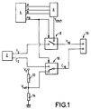
- the video apparatus of figure 1 is a video cassette recorder (VCR) comprising a S-Video source 2 generating a first luminance signal Y 2 and a first chrominance signal C 2 , defining a S-Video signal.
- the S-Video source 2 is a MPEG decoder STI5500 from ST fed by a bit-stream processor SAA6700H from Philips according to data read on a tape in a digital format, for instance D-VHS.
- the S-Video signal is provided by a conventional S-Video circuit of a S-VHS VCR.
- the video apparatus also has an OSD circuit 4 generating three monochrome signals R, G and B (respectively red, green and blue monochrome signals) representing images to be superimposed on the video sequence of the S-Video signals.
- the OSD circuit also generates a fast-blanking signal FB indicating when the monochrome signals R, G and B should be taken into consideration.
- the S-Video source 2 and the OSD circuit 4 co-operate in a conventional manner (not shown) in order to synchronise the fast-blanking signal FB (and thus the monochrome signals R, G and B) with the first luminance signal Y 2 .
- the monochrome signals R, G, and B are converted into a corresponding second luminance signal Y OSD in a converter 6, which can for instance be a resistor matrix network.
- the second luminance signal Y OSD thus represents a black-and-white image of the OSD to be inserted.
- the first luminance signal Y 2 and the second luminance signal Y OSD are respectively transmitted to a first input and to a second input of a first switch 8.
- the first switch 8 is controlled by the fast blanking signal FB to selectively output Y 2 or Y OSD on a first pin of a connector 16.
- the first switch 8 connects the S-Video source 2 to the connector 16 conceming luminance.
- the first switch 8 connects the OSD circuit 4 and converter 6 to the connector 16 to superimpose the balck-and-white image where needed.
- the first switch 8 thus realises the actual OSD insertion.
- a second switch 10 receives on a first pin the first chrominance signal C 2 and on a second pin a constant second chrominance signal V ref .
- the second chrominance signal V ref can be realised by a voltage divider comprising a first resistor 12 and a second resistor 14 in series with ground a constant voltage V 0 (for instance 5 V), the common point of the first and second resistors thus generating the second chrominance signal V ref .
- the second switch 12 is also controlled by the fast-blanking signal FB to selectively output the first chrominance signal C 2 or the second chrominance signal V ref to a second pin of the connector 16.
- the second switch 10 connects the S-Video source 2 to the connector 16 for chrominance.
- the second switch 10 connects the voltage divider to the second pin (chrominance pin C 16 ) of the connector 16, thus setting the second pin of the connector 16 to a predetermined level indicating the signal to be superimposed is black-and-white.
- the first chrominance signal C 2 is not used during OSD insertion ; this avoids an unpleasant color hue which would otherwise be present.
- the connector 16 is meant to deliver at least the S-Video signal with OSD insertion to another video apparatus. It can be of any type, notably a conventional 4-pin S-Video connector or a Scart connector.
- the invention also applies to other types of video apparatus delivering S-Video signals, for instance to DVD players having a S-Video output.
Landscapes
- Engineering & Computer Science (AREA)
- Multimedia (AREA)
- Signal Processing (AREA)
- Computer Graphics (AREA)
- Color Television Systems (AREA)
- Processing Of Color Television Signals (AREA)
- Testing, Inspecting, Measuring Of Stereoscopic Televisions And Televisions (AREA)
- Controls And Circuits For Display Device (AREA)
- Television Signal Processing For Recording (AREA)
Abstract
A video apparatus has a S-Video source (2) with a luminance output
(Y2) carrying a first luminance signal and a chrominance output (C2) carrying a
chrominance signal, an OSD circuit (4) generating OSD signals (R, G, B) and a
fast-blanking signal (FB), and a connector (16) for delivering S-Video signals.
A converter (6) outputs a second luminance signal (YOSD) based on
the OSD signals and a first switch (10) controlled by the fast-blanking signal
(FB) selectively connects the converter (6) or the luminance output (Y2) to the
connector (16)
Preferably, a second switch (10) controlled by the fast-blanking
signal (FB) selectively connects the chrominance output (C2) or a circuit
generating a constant chrominance signal (Vref) to the connector (16).
Description
- The invention relates to a video apparatus delivering S-Video signals.
- S-Video signals are a possible representation of video sequences consisting of a luminance signal (generally referred to as Y) and of a chrominance signal (C). S-Video signals are for instance generated by a S-VHS video cassette recorder (VCR) or by a DVD player having a S-Video output.
- It is always desirable to superimpose images or characters, for instance menus, on the video sequence delivered by the video apparatus : this superimposition is called On-Screen Display (OSD) and is usually sent out of the video apparatus (for instance to a display) as three monochrome signals (RGB format) through a Scart connector.
- Two solutions have already been proposed to output the S-Video signals:
- in a first solution, a dedicated S-Video connector is used ;
- according to a second solution, two pair of pins of the Scart connector are used, specifically the pins conventionally used for the CVBS signal and the pins conventionally used for the red monochrome signal (R).
- With the first solution, as the video signal representing the video sequence goes through the S-Video connector, the video signal can be transmitted, for instance to a display, even when the Scart connector is not used. The user would then be unable to view the menus generated as OSD.
- When using the second solution, the conventional pins for the red monochrome signal are not available and the OSD cannot be displayed properly.
- The invention aims at a video apparatus delivering a S-Video signal which can also transmit OSD information in any circumstance.
- The invention proposes a video apparatus comprising a S-Video source with a luminance output carrying a first luminance signal, an OSD circuit generating OSD signals and a fast-blanking signal, and a connector for delivering S-Video signals, wherein a converter outputs a second luminance signal based on the OSD signals and wherein a first switch controlled by the fast-blanking signal selectively connects the converter or the luminance output to the connector.
- According to preferred features :
- the S-Video source has a chrominance output carrying a chrominance signal and a second switch controlled by the fast-blanking signal selectively connects the chrominance output or a circuit generating a constant chrominance signal to the connector;
- the constant chrominance signal is a constant voltage ;
- a voltage divider generates said constant voltage ;
- said OSD signals are three monochrome signals ;
- said converter is a resistor matrix network.
- The invention and other features thereof will be understood in the light of the following description made with reference to the attached drawings where:
- figure 1 represents a video apparatus realised according to the teachings of the invention.
- The video apparatus of figure 1 is a video cassette recorder (VCR) comprising a S-
Video source 2 generating a first luminance signal Y2 and a first chrominance signal C2, defining a S-Video signal. In the present embodiment, the S-Video source 2 is a MPEG decoder STI5500 from ST fed by a bit-stream processor SAA6700H from Philips according to data read on a tape in a digital format, for instance D-VHS. According to a possible variation, the S-Video signal is provided by a conventional S-Video circuit of a S-VHS VCR. - The video apparatus also has an
OSD circuit 4 generating three monochrome signals R, G and B (respectively red, green and blue monochrome signals) representing images to be superimposed on the video sequence of the S-Video signals. The OSD circuit also generates a fast-blanking signal FB indicating when the monochrome signals R, G and B should be taken into consideration. - Of course, the S-
Video source 2 and theOSD circuit 4 co-operate in a conventional manner (not shown) in order to synchronise the fast-blanking signal FB (and thus the monochrome signals R, G and B) with the first luminance signal Y2. - The monochrome signals R, G, and B are converted into a corresponding second luminance signal YOSD in a converter 6, which can for instance be a resistor matrix network. The second luminance signal YOSD thus represents a black-and-white image of the OSD to be inserted.
- The first luminance signal Y2 and the second luminance signal YOSD are respectively transmitted to a first input and to a second input of a
first switch 8. Thefirst switch 8 is controlled by the fast blanking signal FB to selectively output Y2 or YOSD on a first pin of aconnector 16. - More precisely, when the fast-blanking signal FB is at a low level (meaning no OSD insertion should be realised at this specific moment), the
first switch 8 connects the S-Video source 2 to theconnector 16 conceming luminance. When the fast-blanking signal FB is at a high level, thefirst switch 8 connects theOSD circuit 4 and converter 6 to theconnector 16 to superimpose the balck-and-white image where needed. - The
first switch 8 thus realises the actual OSD insertion. - A
second switch 10 receives on a first pin the first chrominance signal C2 and on a second pin a constant second chrominance signal Vref. As indicated on figure 1, the second chrominance signal Vref can be realised by a voltage divider comprising afirst resistor 12 and asecond resistor 14 in series with ground a constant voltage V0 (for instance 5 V), the common point of the first and second resistors thus generating the second chrominance signal Vref. - The
second switch 12 is also controlled by the fast-blanking signal FB to selectively output the first chrominance signal C2 or the second chrominance signal Vref to a second pin of theconnector 16. - More precisely, when the fast-blanking signal is at a low level, the
second switch 10 connects the S-Video source 2 to theconnector 16 for chrominance. When the fast-blanking signal is at a high level, thesecond switch 10 connects the voltage divider to the second pin (chrominance pin C16) of theconnector 16, thus setting the second pin of theconnector 16 to a predetermined level indicating the signal to be superimposed is black-and-white. - Thanks to the
second switch 10, the first chrominance signal C2 is not used during OSD insertion ; this avoids an unpleasant color hue which would otherwise be present. - The
connector 16 is meant to deliver at least the S-Video signal with OSD insertion to another video apparatus. It can be of any type, notably a conventional 4-pin S-Video connector or a Scart connector. - The invention also applies to other types of video apparatus delivering S-Video signals, for instance to DVD players having a S-Video output.
Claims (6)
- Video apparatus comprising :characterised in thata S-Video source (2) with a luminance output (Y2) carrying a first luminance signal,an OSD circuit (6) generating OSD signals (R, G, B) and a fast-blanking signal (FB), anda connector (16) for delivering S-Video signals,a converter (6) outputs a second luminance signal (YOSD) based on the OSD signals (R, G, B) and in thata first switch (8) controlled by the fast-blanking signal (FB) selectively connects the converter (6) or the luminance output (Y2) to the connector (16).
- Video apparatus according to claim 1, wherein the S-Video source (2) has a chrominance output (C2) carrying a chrominance signal and wherein a second switch (10) controlled by the fast-blanking signal (FB) selectively connects the chrominance output (C2) or a circuit generating a constant chrominance signal (Vref) to the connector (16).
- Video apparatus according to claim 2, wherein the constant chrominance signal is a constant voltage (Vref).
- Video apparatus according to claim 3, wherein a voltage divider (12, 14) generates said constant voltage (Vref).
- Video apparatus according to any of the preceding claims, wherein said OSD signals are three monochrome signals (R, G, B).
- Video apparatus according to any of the preceding claims, wherein said converter (6) is a resistor matrix network.
Priority Applications (8)
| Application Number | Priority Date | Filing Date | Title |
|---|---|---|---|
| EP00402563A EP1189456A1 (en) | 2000-09-15 | 2000-09-15 | Video apparatus delivering a s-video signal |
| AT01120050T ATE411706T1 (en) | 2000-09-15 | 2001-08-21 | DEVICE FOR SUPERLAYING A Y,C VIDEO COMPONENT SIGNAL ON AN OSD SIGNAL |
| EP20010120050 EP1198142B1 (en) | 2000-09-15 | 2001-08-21 | Apparatus for superimposing a Y,C components video signal and an OSD signal |
| DE60136146T DE60136146D1 (en) | 2000-09-15 | 2001-08-21 | Device for superimposing a Y, C video component signal with an OSD signal |
| KR1020010054795A KR100794712B1 (en) | 2000-09-15 | 2001-09-06 | Video device for transmitting video signals, especially S-video signals |
| CNB011328045A CN1208951C (en) | 2000-09-15 | 2001-09-07 | Video-unit for transmission of video signal |
| US09/950,907 US6714255B2 (en) | 2000-09-15 | 2001-09-12 | Video apparatus delivering video signals, notably S-Video signals |
| JP2001280435A JP2002176658A (en) | 2000-09-15 | 2001-09-14 | Video signal, video apparatus outputting especially s- video signal |
Applications Claiming Priority (1)
| Application Number | Priority Date | Filing Date | Title |
|---|---|---|---|
| EP00402563A EP1189456A1 (en) | 2000-09-15 | 2000-09-15 | Video apparatus delivering a s-video signal |
Publications (1)
| Publication Number | Publication Date |
|---|---|
| EP1189456A1 true EP1189456A1 (en) | 2002-03-20 |
Family
ID=8173867
Family Applications (1)
| Application Number | Title | Priority Date | Filing Date |
|---|---|---|---|
| EP00402563A Withdrawn EP1189456A1 (en) | 2000-09-15 | 2000-09-15 | Video apparatus delivering a s-video signal |
Country Status (7)
| Country | Link |
|---|---|
| US (1) | US6714255B2 (en) |
| EP (1) | EP1189456A1 (en) |
| JP (1) | JP2002176658A (en) |
| KR (1) | KR100794712B1 (en) |
| CN (1) | CN1208951C (en) |
| AT (1) | ATE411706T1 (en) |
| DE (1) | DE60136146D1 (en) |
Families Citing this family (4)
| Publication number | Priority date | Publication date | Assignee | Title |
|---|---|---|---|---|
| KR100864720B1 (en) * | 2002-04-15 | 2008-10-23 | 삼성전자주식회사 | Combination system capable of controlling each device through one OSD screen and its operation control method |
| US7707024B2 (en) * | 2002-05-23 | 2010-04-27 | Microsoft Corporation | Method, system, and apparatus for converting currency values based upon semantically labeled strings |
| US7250983B2 (en) * | 2004-08-04 | 2007-07-31 | Trident Technologies, Inc. | System and method for overlaying images from multiple video sources on a display device |
| CN107959867B (en) * | 2016-10-14 | 2020-04-03 | 南宁富桂精密工业有限公司 | Signal generator and set top box with same |
Citations (3)
| Publication number | Priority date | Publication date | Assignee | Title |
|---|---|---|---|---|
| JPH02226893A (en) * | 1989-02-28 | 1990-09-10 | Hitachi Ltd | Magnetic recording and reproducing device |
| JPH06133240A (en) * | 1992-10-20 | 1994-05-13 | Sony Corp | OSD display device |
| JPH10336603A (en) * | 1997-05-28 | 1998-12-18 | Sanyo Electric Co Ltd | Digital television receiver |
Family Cites Families (8)
| Publication number | Priority date | Publication date | Assignee | Title |
|---|---|---|---|---|
| KR970007479B1 (en) * | 1994-06-09 | 1997-05-09 | 삼성전자 주식회사 | Background compensation circuit using on screen display signal |
| KR970005940B1 (en) * | 1994-09-30 | 1997-04-22 | 대우전자 주식회사 | On-Screen Display Unit of Monitor |
| DE69728014T2 (en) * | 1996-05-06 | 2005-01-20 | Koninklijke Philips Electronics N.V. | SIMULTANEOUS PRESENTATION OF A GRAPHIC IMAGE AND A VIDEO IMAGE |
| JP3402076B2 (en) * | 1996-07-01 | 2003-04-28 | 松下電器産業株式会社 | On-screen synthesis circuit for digital broadcast receiver |
| JP3480198B2 (en) * | 1996-10-28 | 2003-12-15 | 松下電器産業株式会社 | Digital broadcast receiver |
| KR19990036008U (en) * | 1998-02-12 | 1999-09-15 | 전주범 | On-Screen Display Control of Complex Satellite Broadcasting System |
| KR19990069714A (en) * | 1998-02-12 | 1999-09-06 | 전주범 | On-Screen Display Control of Complex Satellite Broadcasting System |
| KR19990070245A (en) * | 1998-02-18 | 1999-09-15 | 전주범 | On-Screen Display Control of Complex Satellite Broadcasting System |
-
2000
- 2000-09-15 EP EP00402563A patent/EP1189456A1/en not_active Withdrawn
-
2001
- 2001-08-21 AT AT01120050T patent/ATE411706T1/en not_active IP Right Cessation
- 2001-08-21 DE DE60136146T patent/DE60136146D1/en not_active Expired - Lifetime
- 2001-09-06 KR KR1020010054795A patent/KR100794712B1/en not_active Expired - Fee Related
- 2001-09-07 CN CNB011328045A patent/CN1208951C/en not_active Expired - Fee Related
- 2001-09-12 US US09/950,907 patent/US6714255B2/en not_active Expired - Lifetime
- 2001-09-14 JP JP2001280435A patent/JP2002176658A/en not_active Withdrawn
Patent Citations (3)
| Publication number | Priority date | Publication date | Assignee | Title |
|---|---|---|---|---|
| JPH02226893A (en) * | 1989-02-28 | 1990-09-10 | Hitachi Ltd | Magnetic recording and reproducing device |
| JPH06133240A (en) * | 1992-10-20 | 1994-05-13 | Sony Corp | OSD display device |
| JPH10336603A (en) * | 1997-05-28 | 1998-12-18 | Sanyo Electric Co Ltd | Digital television receiver |
Non-Patent Citations (3)
| Title |
|---|
| PATENT ABSTRACTS OF JAPAN vol. 014, no. 533 (E - 1005) 22 November 1990 (1990-11-22) * |
| PATENT ABSTRACTS OF JAPAN vol. 018, no. 428 (E - 1591) 10 August 1994 (1994-08-10) * |
| PATENT ABSTRACTS OF JAPAN vol. 1999, no. 03 31 March 1999 (1999-03-31) * |
Also Published As
| Publication number | Publication date |
|---|---|
| US20020033898A1 (en) | 2002-03-21 |
| JP2002176658A (en) | 2002-06-21 |
| US6714255B2 (en) | 2004-03-30 |
| CN1208951C (en) | 2005-06-29 |
| DE60136146D1 (en) | 2008-11-27 |
| CN1345163A (en) | 2002-04-17 |
| KR100794712B1 (en) | 2008-01-14 |
| ATE411706T1 (en) | 2008-10-15 |
| KR20020021602A (en) | 2002-03-21 |
Similar Documents
| Publication | Publication Date | Title |
|---|---|---|
| US4814876A (en) | Electronic camera | |
| US5876286A (en) | Game apparatus for television and control method thereof | |
| EP0138482B1 (en) | Video signal superimposing device | |
| US20050122406A1 (en) | Digital camera system and method having autocalibrated playback viewing performance | |
| KR100996622B1 (en) | Video apparatus for detecting video signals and respective methods for recognizing video signals | |
| US6714255B2 (en) | Video apparatus delivering video signals, notably S-Video signals | |
| EP1198142B1 (en) | Apparatus for superimposing a Y,C components video signal and an OSD signal | |
| JP4491164B2 (en) | Video signal transmitter and video signal receiver | |
| KR100769246B1 (en) | Video devices using several video signal sources and methods for controlling such video devices | |
| EP1491057B1 (en) | Video apparatus | |
| EP1271945A2 (en) | Video signal generating apparatus | |
| JPH0646794B2 (en) | Television receiver | |
| EP1187492A1 (en) | Video apparatus having a scart connector and process for controlling such a video apparatus | |
| JP4969629B2 (en) | Video transmission apparatus and video transmission method | |
| JP2517706B2 (en) | Electronics | |
| JP4235796B2 (en) | Electronic camera | |
| KR100310047B1 (en) | Device for inputting and outputting video signal of digital tv | |
| JP3017873B2 (en) | Black and white video signal output device | |
| JP3076412U (en) | Television receiver | |
| JPH0646144Y2 (en) | YC separate input adapter- | |
| JPH0965234A (en) | Television receiver | |
| KR19980029487U (en) | Color Killer Control Unit of Video Cassette Recorder | |
| JPH0888574A (en) | How to adjust electronic devices | |
| JPS635680A (en) | Color television receiver | |
| JP2011147173A (en) | Video signal transmitting device and video signal receiving device |
Legal Events
| Date | Code | Title | Description |
|---|---|---|---|
| PUAI | Public reference made under article 153(3) epc to a published international application that has entered the european phase |
Free format text: ORIGINAL CODE: 0009012 |
|
| AK | Designated contracting states |
Kind code of ref document: A1 Designated state(s): AT BE CH CY DE DK ES FI FR GB GR IE IT LI LU MC NL PT SE |
|
| AX | Request for extension of the european patent |
Free format text: AL;LT;LV;MK;RO;SI |
|
| AKX | Designation fees paid | ||
| REG | Reference to a national code |
Ref country code: DE Ref legal event code: 8566 |
|
| RAP1 | Party data changed (applicant data changed or rights of an application transferred) |
Owner name: THOMSON LICENSING |
|
| STAA | Information on the status of an ep patent application or granted ep patent |
Free format text: STATUS: THE APPLICATION IS DEEMED TO BE WITHDRAWN |
|
| 18D | Application deemed to be withdrawn |
Effective date: 20020921 |