EP1189217A2 - Optical storage element - Google Patents
Optical storage element Download PDFInfo
- Publication number
- EP1189217A2 EP1189217A2 EP01121746A EP01121746A EP1189217A2 EP 1189217 A2 EP1189217 A2 EP 1189217A2 EP 01121746 A EP01121746 A EP 01121746A EP 01121746 A EP01121746 A EP 01121746A EP 1189217 A2 EP1189217 A2 EP 1189217A2
- Authority
- EP
- European Patent Office
- Prior art keywords
- state
- photo
- phase
- transition
- substance
- Prior art date
- Legal status (The legal status is an assumption and is not a legal conclusion. Google has not performed a legal analysis and makes no representation as to the accuracy of the status listed.)
- Withdrawn
Links
Images




Classifications
-
- G—PHYSICS
- G11—INFORMATION STORAGE
- G11B—INFORMATION STORAGE BASED ON RELATIVE MOVEMENT BETWEEN RECORD CARRIER AND TRANSDUCER
- G11B7/00—Recording or reproducing by optical means, e.g. recording using a thermal beam of optical radiation by modifying optical properties or the physical structure, reproducing using an optical beam at lower power by sensing optical properties; Record carriers therefor
- G11B7/24—Record carriers characterised by shape, structure or physical properties, or by the selection of the material
- G11B7/241—Record carriers characterised by shape, structure or physical properties, or by the selection of the material characterised by the selection of the material
- G11B7/242—Record carriers characterised by shape, structure or physical properties, or by the selection of the material characterised by the selection of the material of recording layers
- G11B7/243—Record carriers characterised by shape, structure or physical properties, or by the selection of the material characterised by the selection of the material of recording layers comprising inorganic materials only, e.g. ablative layers
-
- G—PHYSICS
- G11—INFORMATION STORAGE
- G11B—INFORMATION STORAGE BASED ON RELATIVE MOVEMENT BETWEEN RECORD CARRIER AND TRANSDUCER
- G11B11/00—Recording on or reproducing from the same record carrier wherein for these two operations the methods are covered by different main groups of groups G11B3/00 - G11B7/00 or by different subgroups of group G11B9/00; Record carriers therefor
- G11B11/10—Recording on or reproducing from the same record carrier wherein for these two operations the methods are covered by different main groups of groups G11B3/00 - G11B7/00 or by different subgroups of group G11B9/00; Record carriers therefor using recording by magnetic means or other means for magnetisation or demagnetisation of a record carrier, e.g. light induced spin magnetisation; Demagnetisation by thermal or stress means in the presence or not of an orienting magnetic field
- G11B11/105—Recording on or reproducing from the same record carrier wherein for these two operations the methods are covered by different main groups of groups G11B3/00 - G11B7/00 or by different subgroups of group G11B9/00; Record carriers therefor using recording by magnetic means or other means for magnetisation or demagnetisation of a record carrier, e.g. light induced spin magnetisation; Demagnetisation by thermal or stress means in the presence or not of an orienting magnetic field using a beam of light or a magnetic field for recording by change of magnetisation and a beam of light for reproducing, i.e. magneto-optical, e.g. light-induced thermomagnetic recording, spin magnetisation recording, Kerr or Faraday effect reproducing
- G11B11/10582—Record carriers characterised by the selection of the material or by the structure or form
- G11B11/10586—Record carriers characterised by the selection of the material or by the structure or form characterised by the selection of the material
-
- G—PHYSICS
- G11—INFORMATION STORAGE
- G11B—INFORMATION STORAGE BASED ON RELATIVE MOVEMENT BETWEEN RECORD CARRIER AND TRANSDUCER
- G11B5/00—Recording by magnetisation or demagnetisation of a record carrier; Reproducing by magnetic means; Record carriers therefor
- G11B2005/0002—Special dispositions or recording techniques
- G11B2005/0005—Arrangements, methods or circuits
-
- G—PHYSICS
- G11—INFORMATION STORAGE
- G11B—INFORMATION STORAGE BASED ON RELATIVE MOVEMENT BETWEEN RECORD CARRIER AND TRANSDUCER
- G11B5/00—Recording by magnetisation or demagnetisation of a record carrier; Reproducing by magnetic means; Record carriers therefor
- G11B2005/0002—Special dispositions or recording techniques
- G11B2005/0005—Arrangements, methods or circuits
- G11B2005/0021—Thermally assisted recording using an auxiliary energy source for heating the recording layer locally to assist the magnetization reversal
-
- G—PHYSICS
- G11—INFORMATION STORAGE
- G11B—INFORMATION STORAGE BASED ON RELATIVE MOVEMENT BETWEEN RECORD CARRIER AND TRANSDUCER
- G11B7/00—Recording or reproducing by optical means, e.g. recording using a thermal beam of optical radiation by modifying optical properties or the physical structure, reproducing using an optical beam at lower power by sensing optical properties; Record carriers therefor
- G11B7/24—Record carriers characterised by shape, structure or physical properties, or by the selection of the material
- G11B7/241—Record carriers characterised by shape, structure or physical properties, or by the selection of the material characterised by the selection of the material
- G11B7/242—Record carriers characterised by shape, structure or physical properties, or by the selection of the material characterised by the selection of the material of recording layers
- G11B7/243—Record carriers characterised by shape, structure or physical properties, or by the selection of the material characterised by the selection of the material of recording layers comprising inorganic materials only, e.g. ablative layers
- G11B2007/24302—Metals or metalloids
- G11B2007/24306—Metals or metalloids transition metal elements of groups 3-10
-
- G—PHYSICS
- G11—INFORMATION STORAGE
- G11B—INFORMATION STORAGE BASED ON RELATIVE MOVEMENT BETWEEN RECORD CARRIER AND TRANSDUCER
- G11B7/00—Recording or reproducing by optical means, e.g. recording using a thermal beam of optical radiation by modifying optical properties or the physical structure, reproducing using an optical beam at lower power by sensing optical properties; Record carriers therefor
- G11B7/24—Record carriers characterised by shape, structure or physical properties, or by the selection of the material
- G11B7/241—Record carriers characterised by shape, structure or physical properties, or by the selection of the material characterised by the selection of the material
- G11B7/242—Record carriers characterised by shape, structure or physical properties, or by the selection of the material characterised by the selection of the material of recording layers
- G11B7/243—Record carriers characterised by shape, structure or physical properties, or by the selection of the material characterised by the selection of the material of recording layers comprising inorganic materials only, e.g. ablative layers
- G11B2007/24318—Non-metallic elements
- G11B2007/2432—Oxygen
-
- G—PHYSICS
- G11—INFORMATION STORAGE
- G11B—INFORMATION STORAGE BASED ON RELATIVE MOVEMENT BETWEEN RECORD CARRIER AND TRANSDUCER
- G11B7/00—Recording or reproducing by optical means, e.g. recording using a thermal beam of optical radiation by modifying optical properties or the physical structure, reproducing using an optical beam at lower power by sensing optical properties; Record carriers therefor
- G11B7/004—Recording, reproducing or erasing methods; Read, write or erase circuits therefor
- G11B7/0045—Recording
- G11B7/00454—Recording involving phase-change effects
-
- G—PHYSICS
- G11—INFORMATION STORAGE
- G11B—INFORMATION STORAGE BASED ON RELATIVE MOVEMENT BETWEEN RECORD CARRIER AND TRANSDUCER
- G11B7/00—Recording or reproducing by optical means, e.g. recording using a thermal beam of optical radiation by modifying optical properties or the physical structure, reproducing using an optical beam at lower power by sensing optical properties; Record carriers therefor
- G11B7/24—Record carriers characterised by shape, structure or physical properties, or by the selection of the material
- G11B7/241—Record carriers characterised by shape, structure or physical properties, or by the selection of the material characterised by the selection of the material
- G11B7/242—Record carriers characterised by shape, structure or physical properties, or by the selection of the material characterised by the selection of the material of recording layers
- G11B7/244—Record carriers characterised by shape, structure or physical properties, or by the selection of the material characterised by the selection of the material of recording layers comprising organic materials only
- G11B7/249—Record carriers characterised by shape, structure or physical properties, or by the selection of the material characterised by the selection of the material of recording layers comprising organic materials only containing organometallic compounds
Definitions
- the present invention relates to a novel optical storage element for writing and/or erasing information by irradiation with light, and more specifically, to an optical storage element capable of writing and/or erasing information by light and saving electric power in comparison with the current optical storage element.
- One of conventional storage media that carries out writing information by irradiation with light is DVD-RAM.
- a storage apparatus using the DVD-RAM firstly a predetermined position of a storage material of the DVD-RAM is irradiated with light, thereby raising the temperature of the position at least to the melting point thereof. Then, in a cooling process from the raised temperature, the predetermined position is changed from a crystalline state to an amorphous state, thereby writing (or erasing) information to control the information storage.
- irradiation with light has been used to raise the temperature of a material for storage, which requires much energy in irradiation with light to raise the temperature of the material for storage to the melting point thereof.
- the Co-Fe Prussian blue-type complex is capable of bidirectional switching by using lights different in wavelength.
- Fig. 1 shows graphs of magnetization curves of the Prussian blue-type complex, respectively, before irradiation with light as marked by ⁇ (black square), after irradiation with light at 500 to 700 nm in wavelength as marked by ⁇ (black circle), and after irradiation with light at 1319 nm in wevelength as marked by ⁇ (white triangle).
- photo-induced phase-transition phenomena in some other substances such as a spin crossover complex.
- the present invention is an optical storage element capable of writing and/or erasing information by irradiation with light, which element comprises a first unit composed of a first photo-induced phase-transition substance to get stable in a first state and a second unit composed of a second photo-induced phase-transition substance to get stable in a second state, wherein said first and second units are arrayed in a superlattice-like form.
- Fig. 2 is a diagram showing a typical shape of potential of such a substance that shows a photo-induced structural change.
- the substance undergoes transition from a state of stable structure to another state by irradiation with light, and then to still another state, via structural relaxation, to settle.
- An important matter herein is an existence of interaction acting among units within the substance.
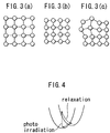
- Figs. 3(a), Fig. 3(b) and Fig. 3(c) show cases where there are two kinds of causes for phase stability. Specifically, they show cases where two kinds of stable lengths of volume expansion, i.e., a distance between atoms.
- the phase of Fig. 3(a), 3(b) and 3(c) are the phases of stable structures.
- the phase of Fig. 3(c) which is a co-existing phase of those of Fig. 3(a) and Fig. 3(b) is unstable because it is energetically disadvantageous between (the boundaries of) the phase of Fig. 3(a) and the phase of Fig. 3(b).
- the substance in the state of co-existing phase of Fig. 3(c) tends to transit to the structural phase either of Fig. 3(a) or Fig. 3(b). This is an example of the cooperative interaction.
- irradiation with light causes a structural change from the phase of Fig. 3(b) to the phase of Fig. 3(a).
- the phase shown in Fig. 3(c) is the phase where one unit of the phase of Fig. 3(b) is changed to the a-state.
- the substance since the co-existing state of two phases such as the phase of Fig. 3(c) is energetically disadvantageous, the substance has a tendency to transit to either the phase of Fig. 3(a) or the phase of Fig. 3(b). However, since there are quite more units in the b-state than in the a-state in number, the substance returns to the phase of Fig. 3(b). Consequently, in order to change the substance from the phase of Fig. 3(b) to the phase of Fig. 3(a), it is necessary to make numerous a-states, which requires a considerable dose of irradiation with light.
- Fig. 4 is a diagram showing a shape of potential in which the life of information storage is shortened, and it shows the difference in energy between two phase-stable structures is great. In this case, a new state produced by irradiation with light returns to its original state by thermal relaxation, which means that the storage of information is to be lost.
- Some spatial units to be used in the present invention are defined as follows.
- the smallest constituent unit is a minimum unit to take the a-state or the b-state. This is called "site.”
- the a-state and the b-state often means a spin state.
- the site means one atom or one molecule that is the unit of one spin.
- unit is used to mean an aggregate of sites of the same kind. Namely, by the unit is meant one square in Fig. 5(a).
- system The largest block discussed in the present invention is called "system", which means the blocks such as shown in Fig. 5(b-1), Fig. 5(b-2), Fig. 6(a), Fig. 6(b) and Fig. 6(c).
- a block becomes a constituent unit for recording one piece of information, and the whole block getting in the a-state or the b-state becomes a record of information.
- the entire system getting integrated into one state is called "phase.”
- a system prepared by artificially combining a plurality of units is called "superlattice system", which is roughly classified into a one-dimensional superlattice, two-dimensional superlattice and three-dimensional superlattice. Examples of these are shown in Figs. 6(a), 6(b) and 6(c).
- Fig. 6(a) shows a one-dimensional superlattice
- Fig. 6(b) a two-dimensional superlattice
- Fig. 6(c) a three-dimensional superlattice, respectively.
- the present invention basically proposes arraying in a superlattice-like form two kinds of substances making photo-induced structural change of such a shape of potential as shown in Fig. 4. This enables to solve the above-mentioned problems.
- Fig. 5(a) shows three kinds of substances having different shapes of potential, in which those substances are aggregates of some sites.
- Fig. 5(b-1) shows the conventional photo-induced phase-transition substance, in which this substance is composed of one unit.
- Fig. 5(b-2) shows an element proposed in this invention, in which two kinds of substances showing photo-induced structural change of different shapes of potential are made into a superlattice form (superstructure).
- a substance having substantially equal a-state energy and b-state energy has been discussed.
- Fig. 5(a) shows photo-induced structural changes of shapes of potential to become stable in either the a-state or the b-state.
- the unit containing a substance which gets stable in the a-state is called ⁇ -unit, and the unit containing a substance to become stable in the b-state is called ⁇ -unit.
- Fig. 5(b-1) shows a conventional homogeneous optical storage element, containing a substance in which the energies in both a-state and b-state are almost equal. In this optical storage element, one piece of information is stored in a cluster composed of several molecules.
- ⁇ -unit and ⁇ -unit are arrayed in a form of superlattice, as plainly shown in Fig. 5(b-2), Fig. 6(a), Fig. 6(b) and Fig. 6(c).
- a cluster as large as the one illustrated in these figures, is stored one piece of information.
- the optical storage element of the present invention may differ in energy in the phase of the a-state and the phase of the b-state, so that choice can be made in a wide range to seek for substances and in material design.
- S i represents a state of i-site and is supposed to take 1/2 when it is in the a-state, while it is supposed to take -1/2 when it is in the b-state.
- ⁇ is to take the sum between nearby atoms (molecules).
- the values are different by J between the case of the same state and the case of a different state.
- the second term shows a tendency for each site.
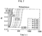
- Fig. 7 shows a phase-transition of a homogeneous cluster composed of 50 ⁇ 50 ⁇ 50 sites, under irradiation with light, and shows the result of calculation regarding the homogeneous system as shown in Fig. 5(b-1).
- the abscissa indicates the time ( ⁇ ) from the beginning of irradiation with light
- the ordinate Rb indicates the ratio of the sites that take the b-state.
- P indicates the amount of absorption of light per unit time, i.e., the intensity of the irradiation with light.
- P 0.140
- P 0.130
- P 0.120
- P 0.120
- P 0.120
- P 0.110
- P 0.100
- Rb remains constant and rapidly increases from a certain time point. This means that, when a location where a site in the b-state reaches a density of a certain degree or above occurs, the location becomes a nuclei and a change to the b-state proceeds rapidly. Also, when the intensity of the irradiation with light is weakened, it takes longer period of time to change into the b-state phase. This is because it takes longer time for formation of the location to become the above-mentioned nuclei. At P ⁇ 0.1, there occurs no change into the b-state phase. This means that without a certain degree of irradiation with light, no transition or change occurs.
- Fig. 8 shows phase-transitions, under the irradiation with light, of a superlattice cluster with 5 ⁇ 5 ⁇ 5 sites as a unit, and shows the result of a calculation regarding the superlattice system as shown in Fig. 5(b-2). It is assumed that one unit is a cube one side of which includes 5 sites, and that the system is a cube with 10 units per side. One system is a cube having 50 sites per side, with ⁇ -units and ⁇ -units mixed in a checker-like pattern. Namely, one system is constituted like the structure shown in Fig. 6(c).
- Fig. 9 shows a superlattice with units having sides alternately different in length.
- D represents a value of energy in an individual site; and D ⁇ and D ⁇ are used to represent the energy in one ⁇ -site and one ⁇ -site, respectively.
- 468 : 532, it is possible to make the total energy of the system equal in both a-state phase and b-state phase by making the length of one side alternately 7, 3, 7, 3....
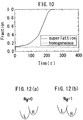
- the solid line denotes the phase-transition under the irradiation with light of the superlattice system shown in Fig. 9.
- This phase transition is a phase transition from the a-state to the b-state, when the entire energy is equal between the phase in a-state and the phase in b-state.
- the dotted line denotes a homogeneous system consisting of only the ⁇ -sites among them.
- a bi-directional phase-transition that is, both the phase transitions from a-state to b-state and from b-state to a-state
- any of the superlattice structures shown in Figs. 6(a), 6(b) and 6(c) is assumed possible in any of the superlattice structures shown in Figs. 6(a), 6(b) and 6(c).
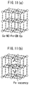
- Figs. 11(a) and 11(b) show the crystalline structures of a Co-Fe Prussian blue analogue.
- Fig. 11(a) shows the structure of a matrix
- Fig. 11(b) shows the structure in which vacancies have taken place of some Fe locations and the cyano groups around them are replaced by water.
- the cyano group that is a ligand is replaced by water, and some kinds of cobalt exist in chemically different environments.
- Figs. 11(a) and 11(b) show the crystalline structures of a Co-Fe Prussian blue analogue.
- Fig. 11(a) shows the structure of a matrix
- Fig. 11(b) shows the structure in which vacancies have taken place of some Fe locations and the cyano groups around them are replaced by water.
- Co-Fe Prussian blue analogue (Co-Fe Prussian blue-type complex), as well as other Prussian blue-type transition metal complexes, are the very realization of the superlattice system to be used in the present invention, as proposed herein by the present inventors.
- perovskite-type manganese oxides can be given as another examples of the photo-induced phase-transition substances to be used in the present invention.
- a homogeneous system using this substance is already patented (Japanese Patent No. 3012902) and is under discussion as a switching system using photo-induced phase transition.
- researches of oxide systems to materialize lamination or superlattice are being carried out by many groups (Lu et al.'s "Magnetoresistance of coherently strained La 2/3 Ba 1/3 MnO 3 /SrTiO 3 superlattices" Physical Review B, Volume 62, No. 23, p.15806 (2000)), and it is assumed that the superlattice structure we proposed herein is also sufficiently realizable.
- the optical storage element may be used, for example, in a form of disk, similarly to a conventional DVD-RAM.
- a method to form the optical storage element of the present invention in disk-like form conventionally known methods can be mentioned.
- an optical storage element that uses a photo-induced phase-transition substance, and that is small in energy consumption, has a long life of information storage, and is capable of writing and/or erasing by irradiation with light, at a high speed, can be provided.
Landscapes
- Chemical & Material Sciences (AREA)
- Inorganic Chemistry (AREA)
- Non-Silver Salt Photosensitive Materials And Non-Silver Salt Photography (AREA)
- Optical Record Carriers And Manufacture Thereof (AREA)
- Semiconductor Memories (AREA)
Abstract
Description

Claims (12)
- An optical storage element capable of writing and/or erasing information by irradiation with light, said element comprising a first unit composed of a first photo-induced phase-transition substance to get stable in a first state and a second unit composed of a second photo-induced phase-transition substance to get stable in a second state, wherein said first and second units are arrayed in a superlattice-like form.
- The optical storage element as claimed in claim 1, wherein at least one of said first photo-induced phase-transition substance and said second photo-induced phase-transition substance is a Prussian blue-type transition metal complex.
- The optical storage element as claimed in claim 1, wherein at least one of said first photo-induced phase-transition substance and said second photo-induced phase-transition substance is a perovskite-type manganese oxide.
- The optical storage element as claimed in claim 1, wherein said first unit and said second unit are arrayed to form a three-dimensional superlattice.
- The optical storage element as claimed in claim 4, wherein at least one of said first photo-induced phase-transition substance and said second photo-induced phase-transition substance is a Prussian blue-type transition metal complex.
- The optical storage element as claimed in claim 4, wherein at least one of said first photo-induced phase-transition substance and said second photo-induced phase-transition substance is a perovskite-type manganese oxide.
- The optical storage element as claimed in claim 1, wherein said first unit and said second unit are arrayed to form a two-dimensional superlattice.
- The optical storage element as claimed in claim 7, wherein at least one of said first photo-induced phase-transition substance and said second photo-induced phase-transition substance is a Prussian blue-type transition metal complex.
- The optical storage element as claimed in claim 7, wherein at least one of said first photo-induced phase-transition substance and said second photo-induced phase-transition substance is a perovskite-type manganese oxide.
- The optical storage element as claimed in claim 1, wherein said first unit and said second unit are arrayed to form a one-dimensional superlattice.
- The optical storage element as claimed in claim 10, wherein at least one of said first photo-induced phase-transition substance and said second photo-induced phase-transition substance is a Prussian blue-type transition metal complex.
- The optical storage element as claimed in claim 10, wherein at least one of said first photo-induced phase-transition substance and said second photo-induced phase-transition substance is a perovskite-type manganese oxide.
Applications Claiming Priority (2)
| Application Number | Priority Date | Filing Date | Title |
|---|---|---|---|
| JP2000282327 | 2000-09-18 | ||
| JP2000282327A JP3564478B2 (en) | 2000-09-18 | 2000-09-18 | Optical storage element |
Publications (2)
| Publication Number | Publication Date |
|---|---|
| EP1189217A2 true EP1189217A2 (en) | 2002-03-20 |
| EP1189217A3 EP1189217A3 (en) | 2003-10-22 |
Family
ID=18766867
Family Applications (1)
| Application Number | Title | Priority Date | Filing Date |
|---|---|---|---|
| EP01121746A Withdrawn EP1189217A3 (en) | 2000-09-18 | 2001-09-18 | Optical storage element |
Country Status (3)
| Country | Link |
|---|---|
| US (1) | US20020048254A1 (en) |
| EP (1) | EP1189217A3 (en) |
| JP (1) | JP3564478B2 (en) |
Families Citing this family (2)
| Publication number | Priority date | Publication date | Assignee | Title |
|---|---|---|---|---|
| JP2005084340A (en) * | 2003-09-08 | 2005-03-31 | Japan Science & Technology Agency | Phase transition method of organic complex and functional element thereof |
| JP2006276453A (en) * | 2005-03-29 | 2006-10-12 | Mitsubishi Chemicals Corp | Information recording medium and optical recording method |
Family Cites Families (2)
| Publication number | Priority date | Publication date | Assignee | Title |
|---|---|---|---|---|
| JP3150331B2 (en) * | 1990-09-28 | 2001-03-26 | 株式会社東芝 | Organic thin film element |
| JP3012902B2 (en) * | 1997-03-18 | 2000-02-28 | 工業技術院長 | Switching device and memory device using photo-induced phase transition |
-
2000
- 2000-09-18 JP JP2000282327A patent/JP3564478B2/en not_active Expired - Lifetime
-
2001
- 2001-09-18 EP EP01121746A patent/EP1189217A3/en not_active Withdrawn
- 2001-09-18 US US09/953,963 patent/US20020048254A1/en not_active Abandoned
Also Published As
| Publication number | Publication date |
|---|---|
| JP2002090939A (en) | 2002-03-27 |
| US20020048254A1 (en) | 2002-04-25 |
| EP1189217A3 (en) | 2003-10-22 |
| JP3564478B2 (en) | 2004-09-08 |
Similar Documents
| Publication | Publication Date | Title |
|---|---|---|
| Zhang et al. | Magnetic skyrmions: materials, manipulation, detection, and applications in spintronic devices | |
| Tudu et al. | Recent developments in perpendicular magnetic anisotropy thin films for data storage applications | |
| JP5122153B2 (en) | Magnetic memory using magnetic domain transfer | |
| Chappert et al. | The emergence of spin electronics in data storage | |
| US7315470B2 (en) | Data storage device and associated method for writing data to, and reading data from an unpatterned magnetic layer | |
| US8614014B2 (en) | Tracks including magnetic layer and magnetic memory devices comprising the same | |
| CN108780779A (en) | Exchange biased utilization type magnetization inversion element, exchange biased utilization type magneto-resistance effect element, exchange biased utilization type magnetic memory, non-volatile logic circuit and magnetic neuron element | |
| US8279653B2 (en) | Magnetic shift register memory in stack structure | |
| US9437269B2 (en) | Antiferromagnetic storage device | |
| US7796415B2 (en) | Magnetic layer, method of forming the magnetic layer, information storage device including the magnetic layer, and method of manufacturing the information storage device | |
| CN1647208A (en) | Synthetic-ferrimagnet sense-layer for high density MRAM applications | |
| KR19990072260A (en) | Limiting magnetoresistive electrical interaction to a preferred portion of a changeable magnetic region in magnetic devices | |
| CN101919000B (en) | Magnetic recording medium | |
| Mejía-López et al. | Asymmetric reversal of the hysteresis loop in exchange-biased nanodots | |
| JP5316967B2 (en) | Magnetic memory element and nonvolatile memory device | |
| WO2002019435A1 (en) | A spin filter and a memory using such a spin filter | |
| CN113039605A (en) | Memory and access method | |
| US20020048254A1 (en) | Optical storage element | |
| Jia et al. | Magnetic sensors for data storage: perspective and future outlook | |
| US8911888B2 (en) | Three-dimensional magnetic memory with multi-layer data storage layers | |
| Campbell et al. | The computer as a materials science benchmark | |
| Yao et al. | Photocontrol of Exchange Bias Using Cobalt–Iron Prussian Blue Analogues for Applications in Spintronics | |
| Editorial Board | GMR: an attractive resistance | |
| DE102009008212B4 (en) | Device with homochiral material component | |
| WINNERS | GMR: An Attractive Resistance |
Legal Events
| Date | Code | Title | Description |
|---|---|---|---|
| PUAI | Public reference made under article 153(3) epc to a published international application that has entered the european phase |
Free format text: ORIGINAL CODE: 0009012 |
|
| 17P | Request for examination filed |
Effective date: 20010918 |
|
| AK | Designated contracting states |
Kind code of ref document: A2 Designated state(s): AT BE CH CY DE DK ES FI FR GB GR IE IT LI LU MC NL PT SE TR |
|
| AX | Request for extension of the european patent |
Free format text: AL;LT;LV;MK;RO;SI |
|
| PUAL | Search report despatched |
Free format text: ORIGINAL CODE: 0009013 |
|
| AK | Designated contracting states |
Kind code of ref document: A3 Designated state(s): AT BE CH CY DE DK ES FI FR GB GR IE IT LI LU MC NL PT SE TR |
|
| AX | Request for extension of the european patent |
Extension state: AL LT LV MK RO SI |
|
| AKX | Designation fees paid |
Designated state(s): AT BE CH CY DE DK ES FI FR GB GR IE IT LI LU MC NL PT SE TR |
|
| STAA | Information on the status of an ep patent application or granted ep patent |
Free format text: STATUS: THE APPLICATION HAS BEEN WITHDRAWN |
|
| 18W | Application withdrawn |
Effective date: 20060831 |