EP1189113A2 - Electrophotosensitive material - Google Patents

Electrophotosensitive material Download PDF

Info

Publication number
EP1189113A2
EP1189113A2 EP01307939A EP01307939A EP1189113A2 EP 1189113 A2 EP1189113 A2 EP 1189113A2 EP 01307939 A EP01307939 A EP 01307939A EP 01307939 A EP01307939 A EP 01307939A EP 1189113 A2 EP1189113 A2 EP 1189113A2
Authority
EP
European Patent Office
Prior art keywords
group
examples
layer
formula
surface protective
Prior art date
Legal status (The legal status is an assumption and is not a legal conclusion. Google has not performed a legal analysis and makes no representation as to the accuracy of the status listed.)
Withdrawn
Application number
EP01307939A
Other languages
German (de)
French (fr)
Other versions
EP1189113A3 (en
Inventor
Eiich c/o Kyocera Mita Corporation Miyamoto
Yoshio c/o Kyocera Mita Corporation Inagaki
Hideaki c/o Kyocera Corporation Fukunaga
Current Assignee (The listed assignees may be inaccurate. Google has not performed a legal analysis and makes no representation or warranty as to the accuracy of the list.)
Kyocera Corp
Kyocera Document Solutions Inc
Original Assignee
Kyocera Corp
Kyocera Mita Corp
Priority date (The priority date is an assumption and is not a legal conclusion. Google has not performed a legal analysis and makes no representation as to the accuracy of the date listed.)
Filing date
Publication date
Priority claimed from JP2000281049A external-priority patent/JP2002091030A/en
Priority claimed from JP2000293942A external-priority patent/JP2002107978A/en
Priority claimed from JP2000293943A external-priority patent/JP2002107979A/en
Priority claimed from JP2000310166A external-priority patent/JP2002116566A/en
Priority claimed from JP2000310165A external-priority patent/JP2002116565A/en
Priority claimed from JP2000338417A external-priority patent/JP2002148836A/en
Application filed by Kyocera Corp, Kyocera Mita Corp filed Critical Kyocera Corp
Publication of EP1189113A2 publication Critical patent/EP1189113A2/en
Publication of EP1189113A3 publication Critical patent/EP1189113A3/en
Withdrawn legal-status Critical Current

Links

Classifications

    • GPHYSICS
    • G03PHOTOGRAPHY; CINEMATOGRAPHY; ANALOGOUS TECHNIQUES USING WAVES OTHER THAN OPTICAL WAVES; ELECTROGRAPHY; HOLOGRAPHY
    • G03GELECTROGRAPHY; ELECTROPHOTOGRAPHY; MAGNETOGRAPHY
    • G03G5/00Recording-members for original recording by exposure, e.g. to light, to heat or to electrons; Manufacture thereof; Selection of materials therefor
    • G03G5/02Charge-receiving layers
    • G03G5/04Photoconductive layers; Charge-generation layers or charge-transporting layers; Additives therefor; Binders therefor
    • G03G5/06Photoconductive layers; Charge-generation layers or charge-transporting layers; Additives therefor; Binders therefor characterised by the photoconductive material being organic
    • G03G5/0664Dyes
    • G03G5/0675Azo dyes
    • G03G5/0677Monoazo dyes
    • GPHYSICS
    • G03PHOTOGRAPHY; CINEMATOGRAPHY; ANALOGOUS TECHNIQUES USING WAVES OTHER THAN OPTICAL WAVES; ELECTROGRAPHY; HOLOGRAPHY
    • G03GELECTROGRAPHY; ELECTROPHOTOGRAPHY; MAGNETOGRAPHY
    • G03G5/00Recording-members for original recording by exposure, e.g. to light, to heat or to electrons; Manufacture thereof; Selection of materials therefor
    • G03G5/02Charge-receiving layers
    • G03G5/04Photoconductive layers; Charge-generation layers or charge-transporting layers; Additives therefor; Binders therefor
    • G03G5/06Photoconductive layers; Charge-generation layers or charge-transporting layers; Additives therefor; Binders therefor characterised by the photoconductive material being organic
    • G03G5/0601Acyclic or carbocyclic compounds
    • G03G5/0605Carbocyclic compounds
    • GPHYSICS
    • G03PHOTOGRAPHY; CINEMATOGRAPHY; ANALOGOUS TECHNIQUES USING WAVES OTHER THAN OPTICAL WAVES; ELECTROGRAPHY; HOLOGRAPHY
    • G03GELECTROGRAPHY; ELECTROPHOTOGRAPHY; MAGNETOGRAPHY
    • G03G5/00Recording-members for original recording by exposure, e.g. to light, to heat or to electrons; Manufacture thereof; Selection of materials therefor
    • G03G5/02Charge-receiving layers
    • G03G5/04Photoconductive layers; Charge-generation layers or charge-transporting layers; Additives therefor; Binders therefor
    • G03G5/06Photoconductive layers; Charge-generation layers or charge-transporting layers; Additives therefor; Binders therefor characterised by the photoconductive material being organic
    • G03G5/0601Acyclic or carbocyclic compounds
    • G03G5/0609Acyclic or carbocyclic compounds containing oxygen
    • GPHYSICS
    • G03PHOTOGRAPHY; CINEMATOGRAPHY; ANALOGOUS TECHNIQUES USING WAVES OTHER THAN OPTICAL WAVES; ELECTROGRAPHY; HOLOGRAPHY
    • G03GELECTROGRAPHY; ELECTROPHOTOGRAPHY; MAGNETOGRAPHY
    • G03G5/00Recording-members for original recording by exposure, e.g. to light, to heat or to electrons; Manufacture thereof; Selection of materials therefor
    • G03G5/02Charge-receiving layers
    • G03G5/04Photoconductive layers; Charge-generation layers or charge-transporting layers; Additives therefor; Binders therefor
    • G03G5/06Photoconductive layers; Charge-generation layers or charge-transporting layers; Additives therefor; Binders therefor characterised by the photoconductive material being organic
    • G03G5/0601Acyclic or carbocyclic compounds
    • G03G5/0612Acyclic or carbocyclic compounds containing nitrogen
    • G03G5/0616Hydrazines; Hydrazones
    • GPHYSICS
    • G03PHOTOGRAPHY; CINEMATOGRAPHY; ANALOGOUS TECHNIQUES USING WAVES OTHER THAN OPTICAL WAVES; ELECTROGRAPHY; HOLOGRAPHY
    • G03GELECTROGRAPHY; ELECTROPHOTOGRAPHY; MAGNETOGRAPHY
    • G03G5/00Recording-members for original recording by exposure, e.g. to light, to heat or to electrons; Manufacture thereof; Selection of materials therefor
    • G03G5/02Charge-receiving layers
    • G03G5/04Photoconductive layers; Charge-generation layers or charge-transporting layers; Additives therefor; Binders therefor
    • G03G5/06Photoconductive layers; Charge-generation layers or charge-transporting layers; Additives therefor; Binders therefor characterised by the photoconductive material being organic
    • G03G5/0622Heterocyclic compounds
    • G03G5/0624Heterocyclic compounds containing one hetero ring
    • G03G5/0627Heterocyclic compounds containing one hetero ring being five-membered
    • G03G5/0631Heterocyclic compounds containing one hetero ring being five-membered containing two hetero atoms
    • GPHYSICS
    • G03PHOTOGRAPHY; CINEMATOGRAPHY; ANALOGOUS TECHNIQUES USING WAVES OTHER THAN OPTICAL WAVES; ELECTROGRAPHY; HOLOGRAPHY
    • G03GELECTROGRAPHY; ELECTROPHOTOGRAPHY; MAGNETOGRAPHY
    • G03G5/00Recording-members for original recording by exposure, e.g. to light, to heat or to electrons; Manufacture thereof; Selection of materials therefor
    • G03G5/02Charge-receiving layers
    • G03G5/04Photoconductive layers; Charge-generation layers or charge-transporting layers; Additives therefor; Binders therefor
    • G03G5/06Photoconductive layers; Charge-generation layers or charge-transporting layers; Additives therefor; Binders therefor characterised by the photoconductive material being organic
    • G03G5/0622Heterocyclic compounds
    • G03G5/0624Heterocyclic compounds containing one hetero ring
    • G03G5/0635Heterocyclic compounds containing one hetero ring being six-membered
    • G03G5/0638Heterocyclic compounds containing one hetero ring being six-membered containing two hetero atoms
    • GPHYSICS
    • G03PHOTOGRAPHY; CINEMATOGRAPHY; ANALOGOUS TECHNIQUES USING WAVES OTHER THAN OPTICAL WAVES; ELECTROGRAPHY; HOLOGRAPHY
    • G03GELECTROGRAPHY; ELECTROPHOTOGRAPHY; MAGNETOGRAPHY
    • G03G5/00Recording-members for original recording by exposure, e.g. to light, to heat or to electrons; Manufacture thereof; Selection of materials therefor
    • G03G5/02Charge-receiving layers
    • G03G5/04Photoconductive layers; Charge-generation layers or charge-transporting layers; Additives therefor; Binders therefor
    • G03G5/06Photoconductive layers; Charge-generation layers or charge-transporting layers; Additives therefor; Binders therefor characterised by the photoconductive material being organic
    • G03G5/0622Heterocyclic compounds
    • G03G5/0624Heterocyclic compounds containing one hetero ring
    • G03G5/0635Heterocyclic compounds containing one hetero ring being six-membered
    • G03G5/064Heterocyclic compounds containing one hetero ring being six-membered containing three hetero atoms
    • GPHYSICS
    • G03PHOTOGRAPHY; CINEMATOGRAPHY; ANALOGOUS TECHNIQUES USING WAVES OTHER THAN OPTICAL WAVES; ELECTROGRAPHY; HOLOGRAPHY
    • G03GELECTROGRAPHY; ELECTROPHOTOGRAPHY; MAGNETOGRAPHY
    • G03G5/00Recording-members for original recording by exposure, e.g. to light, to heat or to electrons; Manufacture thereof; Selection of materials therefor
    • G03G5/02Charge-receiving layers
    • G03G5/04Photoconductive layers; Charge-generation layers or charge-transporting layers; Additives therefor; Binders therefor
    • G03G5/06Photoconductive layers; Charge-generation layers or charge-transporting layers; Additives therefor; Binders therefor characterised by the photoconductive material being organic
    • G03G5/0622Heterocyclic compounds
    • G03G5/0644Heterocyclic compounds containing two or more hetero rings
    • GPHYSICS
    • G03PHOTOGRAPHY; CINEMATOGRAPHY; ANALOGOUS TECHNIQUES USING WAVES OTHER THAN OPTICAL WAVES; ELECTROGRAPHY; HOLOGRAPHY
    • G03GELECTROGRAPHY; ELECTROPHOTOGRAPHY; MAGNETOGRAPHY
    • G03G5/00Recording-members for original recording by exposure, e.g. to light, to heat or to electrons; Manufacture thereof; Selection of materials therefor
    • G03G5/02Charge-receiving layers
    • G03G5/04Photoconductive layers; Charge-generation layers or charge-transporting layers; Additives therefor; Binders therefor
    • G03G5/06Photoconductive layers; Charge-generation layers or charge-transporting layers; Additives therefor; Binders therefor characterised by the photoconductive material being organic
    • G03G5/0622Heterocyclic compounds
    • G03G5/0644Heterocyclic compounds containing two or more hetero rings
    • G03G5/0646Heterocyclic compounds containing two or more hetero rings in the same ring system
    • G03G5/0651Heterocyclic compounds containing two or more hetero rings in the same ring system containing four relevant rings
    • GPHYSICS
    • G03PHOTOGRAPHY; CINEMATOGRAPHY; ANALOGOUS TECHNIQUES USING WAVES OTHER THAN OPTICAL WAVES; ELECTROGRAPHY; HOLOGRAPHY
    • G03GELECTROGRAPHY; ELECTROPHOTOGRAPHY; MAGNETOGRAPHY
    • G03G5/00Recording-members for original recording by exposure, e.g. to light, to heat or to electrons; Manufacture thereof; Selection of materials therefor
    • G03G5/14Inert intermediate or cover layers for charge-receiving layers
    • G03G5/147Cover layers
    • G03G5/14704Cover layers comprising inorganic material

Definitions

  • the present invention relates to an electrophotosensitive material.
  • organic electrophotosensitive material As an electrophotosensitive material for use in image forming apparatuses such as electrostatic copiers, laser beam printers, plain paper facsimiles and the like, a so-called organic electrophotosensitive material is widespread which comprises a combination of the following components:
  • the charge transport materials fall into two broad categories which include a positive-hole transport material for transporting positive holes of the electric charge, and an electron transport material for transporting electrons.
  • the organic electrophotosensitive material has an advantage over an inorganic electrophotosensitive material employing an inorganic semiconductor material in that the organic electrophotosensitive material is fabricated more easily at less production costs than the latter.
  • the organic electrophotosensitive material also has a merit of greater freedom of function design by virtue of a wide variety of options for materials including charge generating materials, charge transport materials, binder resins and the like.
  • the organic electrophotosensitive material is constructed by forming a single-layer or multi-layer photosensitive layer over a conductive substrate.
  • the single-layer photosensitive layer is formed by dispersing a charge generating material and a charge transport material (a positive-hole transport material and/or an electron transport material) in a binder resin.
  • the multi-layer photosensitive layer is formed by forming a lamination of the charge generating layer containing the charge generating material and the charge transport layer containing the charge transport material (the positive-hole transport material or the electron transport material).
  • the organic electrophotosensitive material is susceptible to scratches, marks and the like in an actual use environment, thus suffering a smaller durability than the inorganic electrophotosensitive material.
  • the widely used surface protective layer is exemplified by an organic layer which is preferable in the light of adhesion to and affinity with the organic photosensitive layer, integrity as a lamination, and consistency in the film forming process.
  • a usable surface protective layer includes, for example, a layer of binder resin, and a layer of binder resin having conductive particles, such as of metal oxides, dispersed therein.
  • the electrophotosensitive material employing such an organic layer as the surface protective layer suffers the drawbacks of an increased residual potential and a lowered chargeability when repeatedly used for image forming processes, and of significant variations in the photosensitivity characteristics due to environmental changes (temperature, humidity and the like).
  • an inorganic layer as the surface protective layer
  • the inorganic layer comprising an inorganic material such as metallic elements, carbon and inorganic compounds containing any of these elements, and having high hardness and wear resistance.
  • the inorganic surface protective layer may be laid over the organic photosensitive layer by, for example, the vapor deposition method such as sputtering, plasma CVD, photo CVD or the like.
  • the inorganic surface protective layer is employed for the purposes of protecting the organic photosensitive layer and overcoming the above problem.
  • the electrophotosensitive material with the inorganic surface protective layer laid over the organic photosensitive layer has functions associated with the characteristics of the individual layers thereof, the organic photosensitive layer involved in the generation and transport of the electric charge, the surface protective layer responsible for ensuring the good durability and environmental resistance.
  • the inorganic surface protective layer has a lower ability to achieve a sufficient adhesion to the organic photosensitive layer. Even if adjustments for the deposition process or the deposition conditions may provide the inorganic layer with a sufficient initial adhesion to the organic layer, the inorganic layer is prone to suffer cracks or delamination due to various stresses imposed thereon under the actual use environment or during the long-term storage thereof.
  • the organic photosensitive layer and the inorganic surface protective layer which are formed of different materials, there are not attained as good adhering relation, affinity and integrity as in the combination of the organic layers or of the inorganic layers. That is, the organic layer and the inorganic layer are often merely combined with each other through a very small binding strength.
  • the electrophotosensitive material when subjected to mechanical stresses such as of contact pressure from a cleaning blade of the image forming apparatus, or thermal stresses due to repeated cycles of heating during the operation of the apparatus and cooling during the nonoperation thereof, or temperature changes during storage, the electrophotosensitive material will suffer cracks in the inorganic surface protective layer or delamination of the surface protective layer from the organic photosensitive layer as a result of increased differences between the hardnesses, flexibilities, expansion/shrinkage properties or the like of these layers.
  • the conventional inorganic surface protective layer is yet to be put to practical use because it has not achieved a sufficient effect to increase the durability of the organic photosensitive layer.
  • the present invention seeks to provide an organic electrophotosensitive material comprising an inorganic surface protective layer less prone to suffer cracks or delamination and excellent in physical stability, thereby achieving a greater durability as compared with the prior-art products.
  • the inventors have analyzed and investigated the film forming process for the inorganic surface protective layer.
  • the inorganic material forming the surface protective layer is somehow combined with a part of the material of the organic photosensitive layer that is exposed at the outermost part thereof, thereby forming a nucleus for film growth.
  • a film of the inorganic material grows about the resultant nucleus and thus, the surface protective layer is formed.
  • the nucleus portion functions as a binding point with the organic photosensitive layer, ensuring the good adhesion between these layers.
  • the magnitude of binding strength between the organic photosensitive layer and the inorganic material at individual binding points as well as the per-area number of binding points namely the density of the binding points at an interface between the organic photosensitive layer and the surface protective layer give significant influences on the adhesion of the surface protective layer to the organic photosensitive layer and the physical stability of the surface protective layer.
  • the surface protective layer is accordingly increased in the adhesion to the organic photosensitive layer, resulting in the greater physical stability.
  • the typical organic photosensitive layer has a structure wherein low molecular weight functional materials including the charge generating material, charge transport material and the like are dispersed in the binder resin forming the layer.
  • the binder resin forming the layer and accounting for a major part thereof, acts as the nucleus of film growth so as to be combined with the inorganic material forming the surface protective layer.
  • the formation of the surface protective layer proceeds with some of the low molecular weight materials, that is exposed at the outermost part of the organic photosensitive layer, functioning as the nuclei of film growth, the low-molecular weight materials including the charge generating material, charge transport material and the like which are dispersed in the layer.
  • the properties of the low molecular weight materials which include the reactivity and binding strength with the inorganic material, the degrees of the compatibility and affinity with the binder resin forming the organic photosensitive layer, the dimensions of the materials themselves (including not only the molecular weight but also the molecular or spatial extent), also significantly affect the adhesion to the organic photosensitive layer and the physical stability of the surface protective layer.
  • the surface protective layer is accordingly improved in the adhesion to the organic photosensitive layer and in the physical stability thereof.
  • the low molecular weight materials are increased in the compatibility and affinity with the binder resin forming the organic photosensitive layer as well as in the dimensions thereof, a so-called anchor effect is accordingly increased so that the surface protective layer is also improved in the adhesion to the organic photosensitive layer and the physical stability thereof.
  • the most preferred is molecular bond in the light of the magnitude of the binding strength.
  • this bond should change the molecular structure to cause the production of an electric charge trap, the photosensitivity of the electrophotosensitive material might be decreased.
  • a electrophotosensitive material capable of forming preferable images cannot be obtained simply by overlaying on the conventional organic photosensitive layer a surface protective layer containing an inorganic material of a greater hardness.
  • the inorganic surface protective layer contributes to the improvement of the durability and environmental resistance of the electrophotosensitive material while maintaining the electrical characteristics of the organic photosensitive layer as they are.
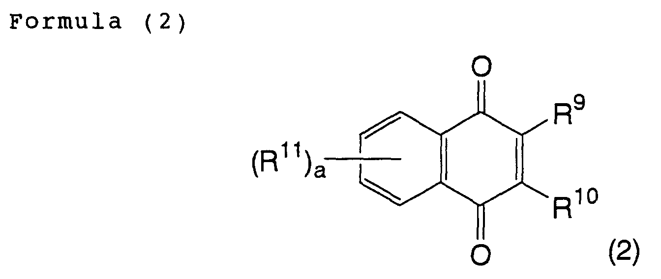
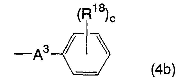
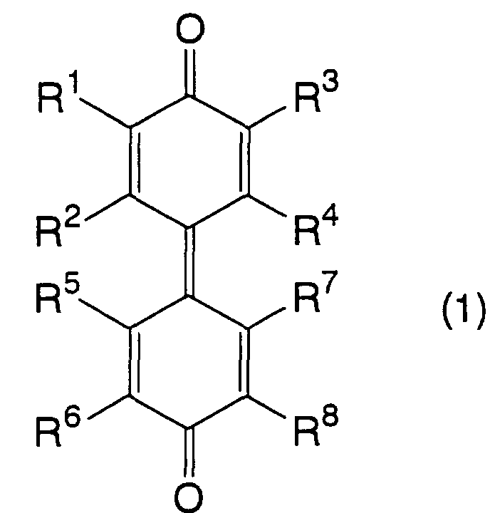
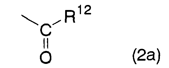
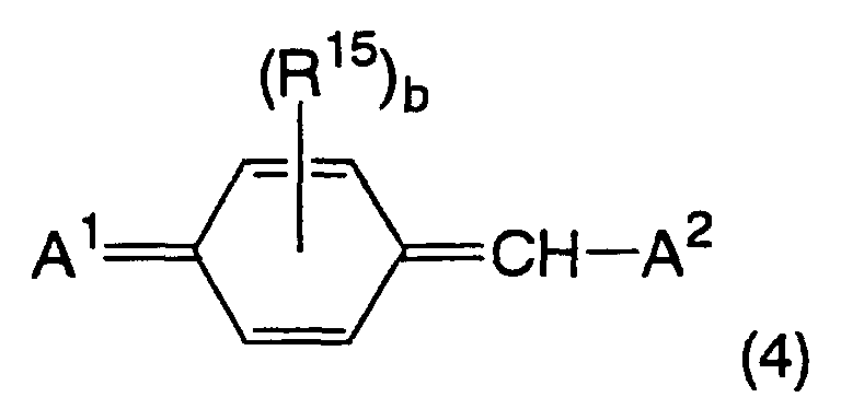
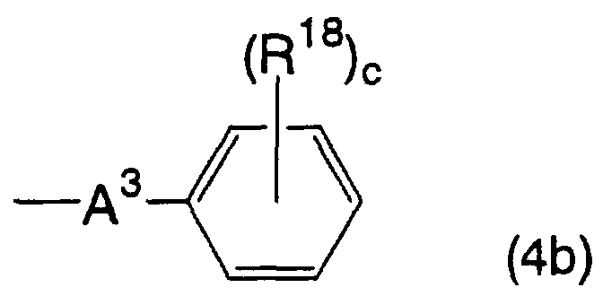
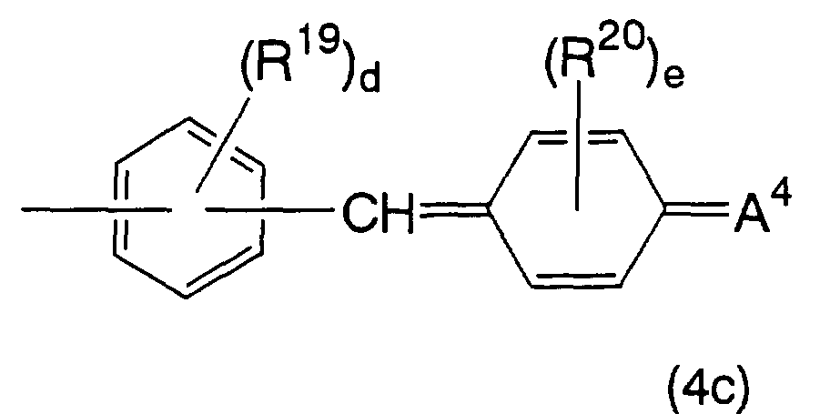
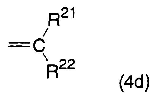
  • a suitable material satisfying these requirements is a compound represented by any one of the following formulas (1) to (4): wherein R 1 , R 2 , R 3 , R 4 , R 5 , R 6 , R 7 and R 8 are the same or different and each denoting a hydrogen atom, alkyl group, alkoxy group, aryl group, cycloalkyl group or aralkyl group; and out of the groups R 1 to R 8 , two groups bonded to adjacent carbon atoms of the same ring may be linked together to form a condensed ring jointly with the ring; wherein R 9 and R 10 are the same or different and each denoting a hydrogen atom, alkyl group, alkoxy group, alkylthio group, aryl group, cycloalkyl group, aryloxy group, arylthio group or a group represented
  • the electrophotosensitive material of the invention comprises the organic photosensitive layer and the inorganic surface protective layer laid over the conductive substrate in this order, wherein at least an outermost part of the organic photosensitive layer that contacts the surface protective layer contains at least one compound selected from the group consisting of a diphenoquinone derivative of the formula (1), a naphthoquinone derivative of the formula (2), a naphthylene diimide derivative of the formula (3) and a quinone derivative of the formula (4).
  • the above compounds each feature a great reactivity with the inorganic material forming the surface protective layer because a ⁇ -electron conjugated system is spread across the molecules thereof so that the compounds has a function to attract particularly a metallic element or carbon of the inorganic material at the initial stage of the film forming process.
  • this function increases the ratio of the molecules of these compounds exposed at the outermost part of the organic photosensitive layer that are combined with the inorganic material to form the nuclei of film growth. This results in a higher density of the binding points at the interface between these layers.
  • the higher the density of the binding points the greater the film growth rate. Therefore, the time for film forming process may be reduced thereby minimizing damage on the organic photosensitive layer during the deposition of the surface protective layer by the vapor deposition method or the like.
  • each of the above compounds is rigidly combined with a metallic element, carbon or the like via molecular bond.
  • a metallic element carbon or the like via molecular bond.
  • This provides a dipolar resonance structure wherein carbon has a positive polarity while oxygen or the group A 1 has a negative polarity.
  • the compound is increased in reactivity, contributing to a significant increase in the binding strength between the organic photosensitive layer and the inorganic material.
  • each of the compounds has a molecular structure spread in a plane-like fashion as a whole, thus having a great molecular or spatial extent. Furthermore, the compounds are all excellent in compatibility and affinity with the binder resin, presenting a good anchor effect on the binder resin.
  • the physical stability of the inorganic surface protective layer may be improved by increasing the adhesion thereof to the organic photosensitive layer.
  • the surface protective layer may be prevented from suffering the occurrence of cracks and delamination in the actual use environment or during the long-term storage.
  • the electrophotosensitive material featuring a superior durability to the conventional ones may be provided.
  • the compounds do not produce a deep electric charge trap even when they are changed in the molecular structures thereof due to the molecular bond with a metal or carbon.
  • the molecular bond occurs only in a limited part of the compound that is exposed at the outermost part of the organic photosensitive layer, so that a major part of the compound in the organic photosensitive layer maintains its initial state as it is. Hence, there is no fear of reducing the photosensitivity of the electrophotosensitive material.
  • the electrophotosensitive material of the invention also features good photosensitivity characteristics.
  • At least an outermost part of an organic photosensitive layer that is in contact with a surface protective layer contains any one of the above compounds represented by the formulas (1) to (4).
  • alkyl group in the above formulas examples include alkyl groups having 1 to 12 carbon atoms, such as methyl, ethyl, n-propyl (n-Pr), isopropyl (i-Pr), n-butyl (n-Bu), isobutyl (i-Bu), sec-butyl (s-Bu), tert-butyl(t-Bu), pentyl(n-amyl), isopentyl (isoamyl), sec-amyl, tert-amyl, neopentyl, hexyl, heptyl, octyl, nonyl, decyl, undecyl, dodecyl and the like.
  • alkyl groups having 1 to 12 carbon atoms such as methyl, ethyl, n-propyl (n-Pr), isopropyl (i-Pr), n-butyl (n-Bu), isobutyl (i
  • alkoxy group examples include alkoxy groups having 1 to 12 carbon atoms, such as methoxy, ethoxy, n-propoxy, isopropoxy, n-butoxy, isobutoxy, sec-butoxy, tert-butoxy, pentyloxy, isopentyloxy, neopentyloxy, hexyloxy, heptyloxy, octyloxy, nonyloxy, decyloxy, undecyloxy, dodecyloxy and the like.
  • alkoxy groups having 1 to 12 carbon atoms such as methoxy, ethoxy, n-propoxy, isopropoxy, n-butoxy, isobutoxy, sec-butoxy, tert-butoxy, pentyloxy, isopentyloxy, neopentyloxy, hexyloxy, heptyloxy, octyloxy, nonyloxy, decyloxy, undecyloxy
  • aryl group examples include groups derived from aromatic compounds such as benzene, toluene, xylene, biphenyl, o-terphenyl, m-terphenyl, p-terphenyl, naphthalene, anthracene, phenanthrene, pyrene, indene, azulene, heptalene, biphenylene, fluorene and the like.
  • aralkyl group examples include aralkyl groups having 4 to 10 carbon atoms in an aryl potion thereof, such as benzyl, benzhydryl, triphenylmethyl, phenethyl, thenyl, furfuryl and the like.
  • alkylthio group examples include those represented by -S-R a wherein R a denotes the above alkyl group having 1 to 12 carbon atoms.
  • aryloxy group examples include those represented by -O- ⁇ 1 wherein ⁇ 1 denotes the aforesaid aryl group.
  • arylthio group examples include those represented by -S- ⁇ 2 wherein ⁇ 2 denotes the aforesaid aryl group.
  • alkoxycarbonyl group examples include those represented by -COOR b wherein R b denotes the above alkyl group having 1 to 12 carbon atoms.
  • cycloalkyl group examples include cycloalkyl groups having 5 to 12 carbon atoms, such as cyclopentyl, cyclohexyl, 1-cyclohexenyl, cycloheptyl, cyclooctyl, cyclononyl, cyclodecyl, cycloundecyl, cyclododecyl and the like.
  • heterocyclic group examples include such as thienyl, furyl, pyrrolyl, pyrrolidinyl, oxazoly, isoxazolyl, thiazolyl, isothiazolyl, imidazolyl, 2H-imidazolyl, piperidyl, piperidino, 3-morpholinyl, morpholino and the like.
  • it may be a heterocyclic group condensed with an aromatic ring.
  • substituents may be unsubstituted or contain one or more substituents which are exemplified by the above groups and halogen atoms.
  • Other usable substituents include, for example, hydroxyalkyl groups; alkoxyalkyl groups; monoalkyl aminoalkyl groups; dialkyl aminoalkyl groups; halogen-substituted alkyl groups; alkoxycarbonylalkyl groups; carboxyalkyl groups; alkanoyloxyalkyl groups; aminoalkyl groups; amino group; hydroxy group; optionally esterified carboxyl groups; cyano group, nitro group and the like.
  • the substituents are not particularly limited in the position and the number.
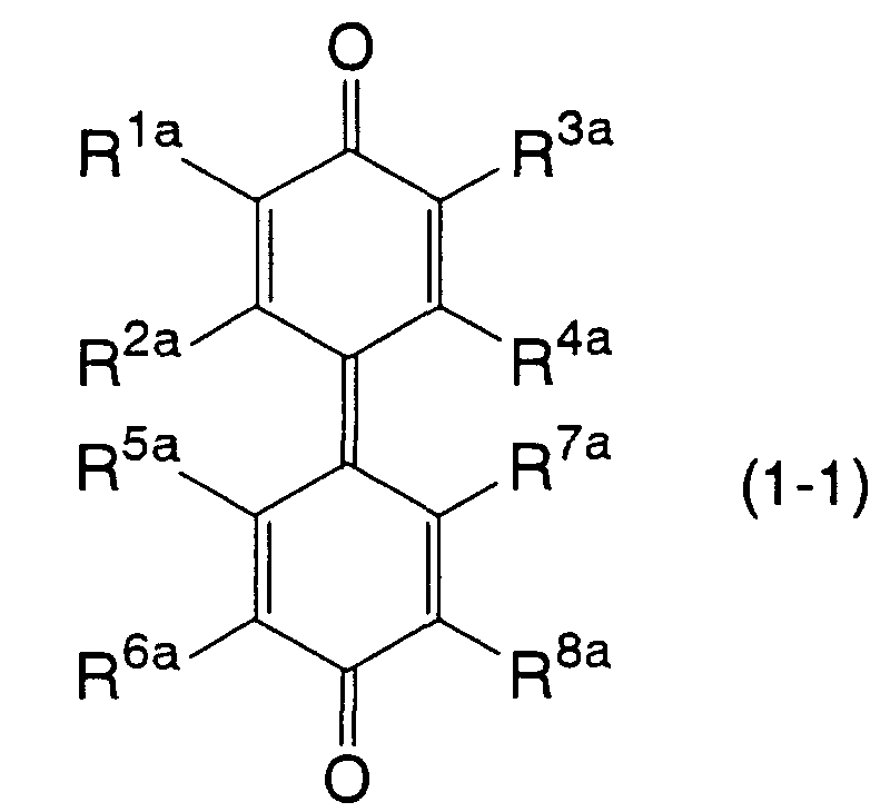
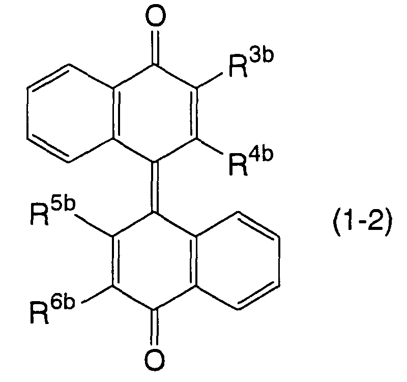
  • an example of a preferred diphenoquinone derivative of the formula (1) includes at least one selected from the group consisting of a diphenoquinone compound represented by a formula (1-1): wherein R 1a , R 2a , R 3a , R 4a , R 5a , R 6a , R 7a and R 8a are the same or different and each denoting a hydrogen atom, alkyl group, alkoxy group, aryl group, cycloalkyl group or aralkyl group; and a dinaphthoquinone compound represented by a formula (1-2): wherein R 3b , R 4b , R 5b and R 6b are the same or different and each denoting a hydrogen atom, alkyl group, alkoxy group, aryl group, cycloalkyl group or aralkyl group.
  • a diphenoquinone compound represented by a formula (1-1) wherein R 1a , R 2a , R 3a ,
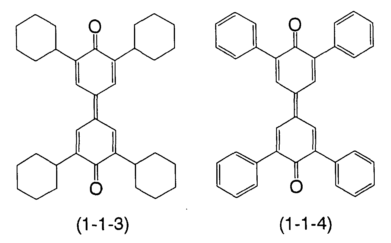
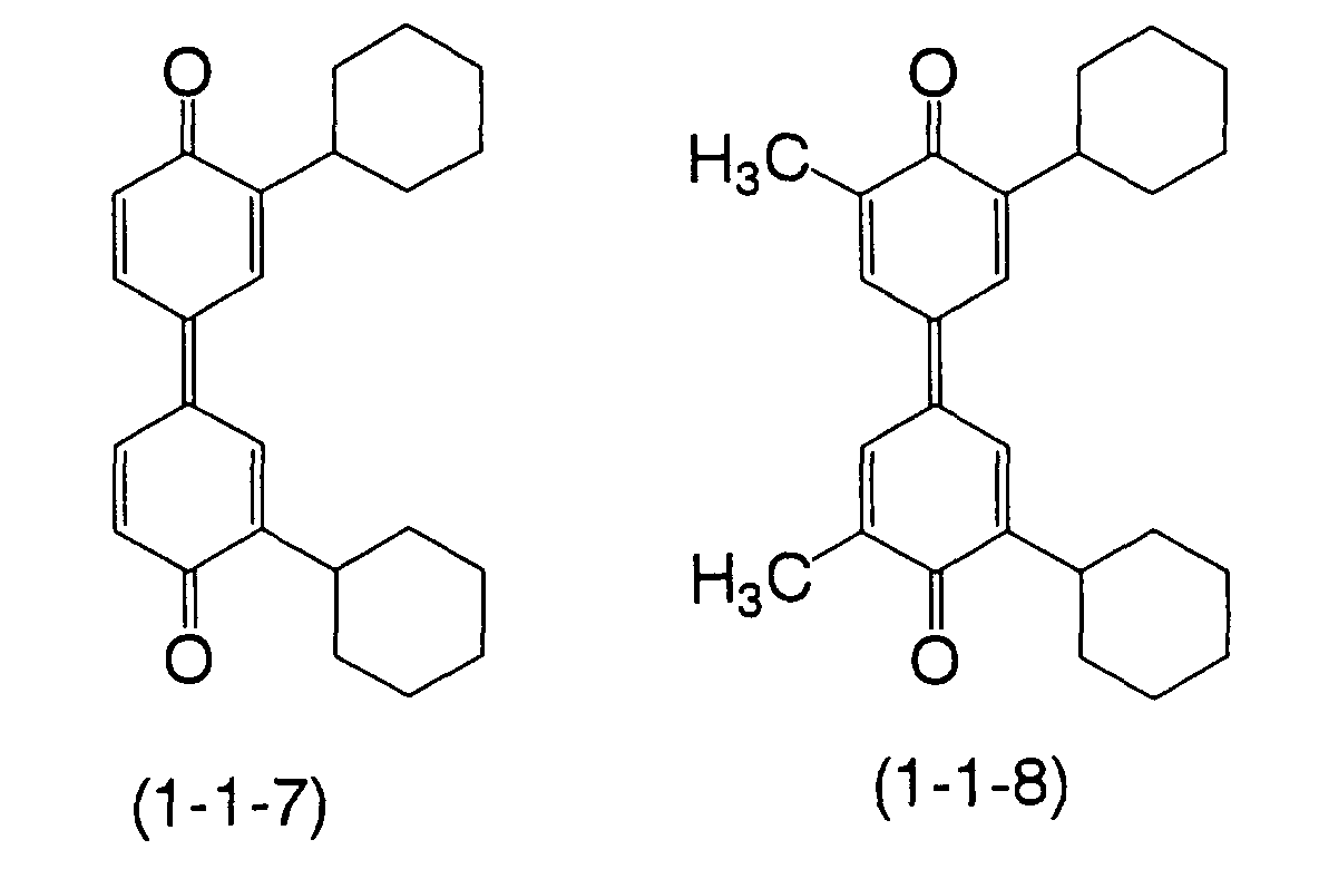
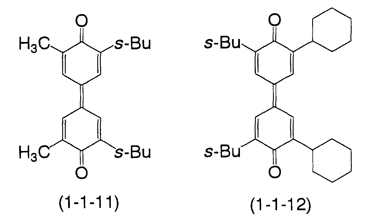
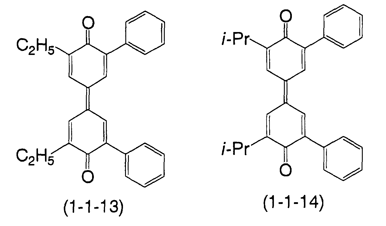
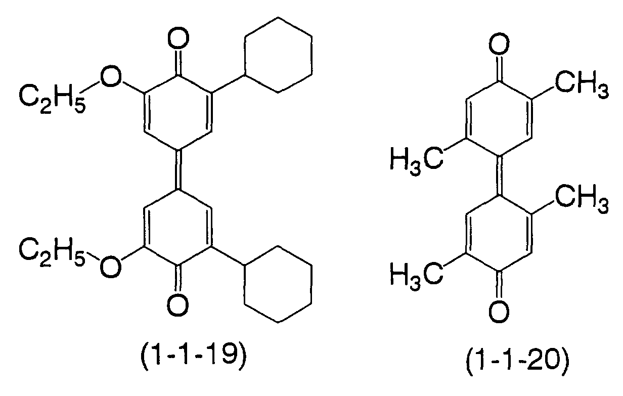
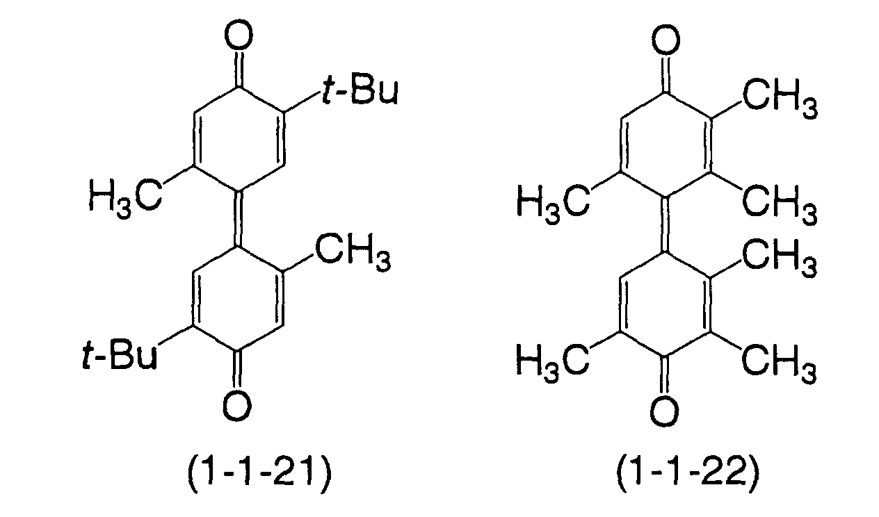
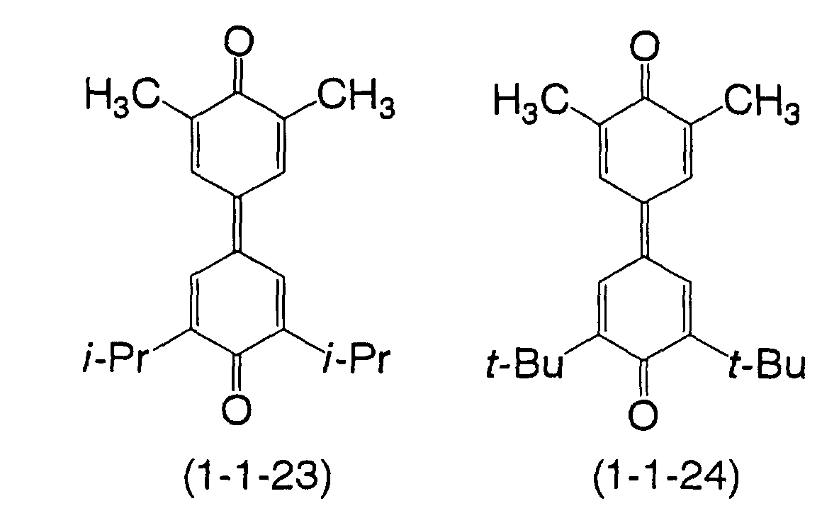
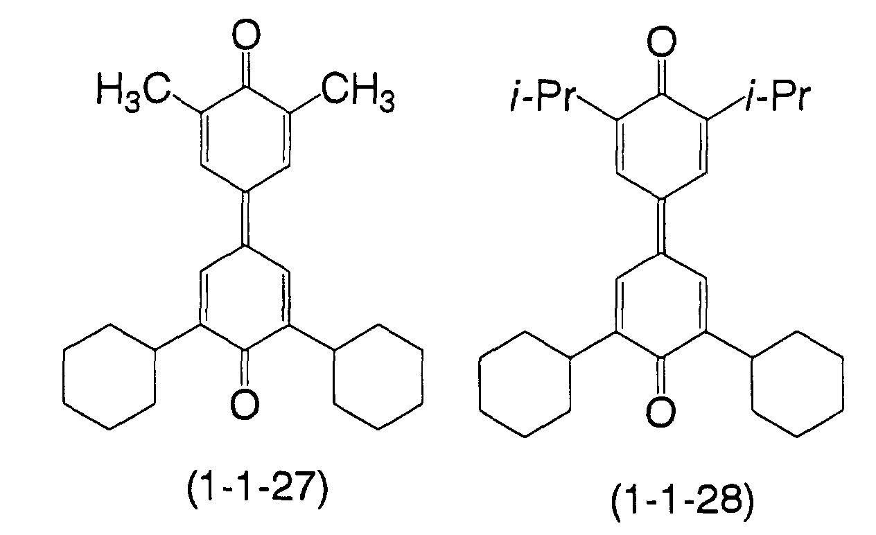
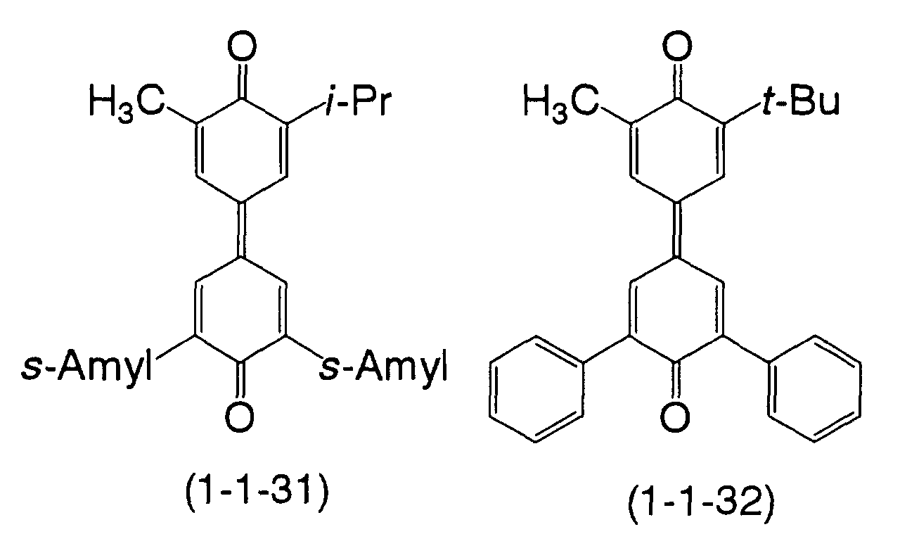
  • diphenoquinone compound of the formula (1-1) include compounds represented by formulas (1-1-1) to (1-1-32).
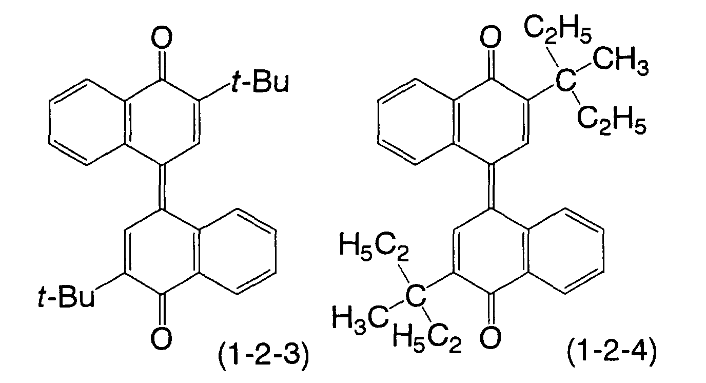
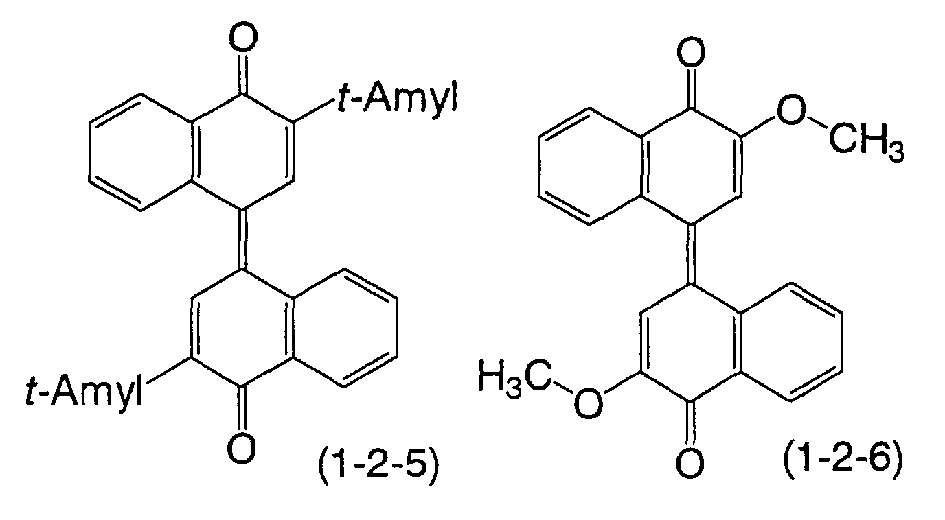
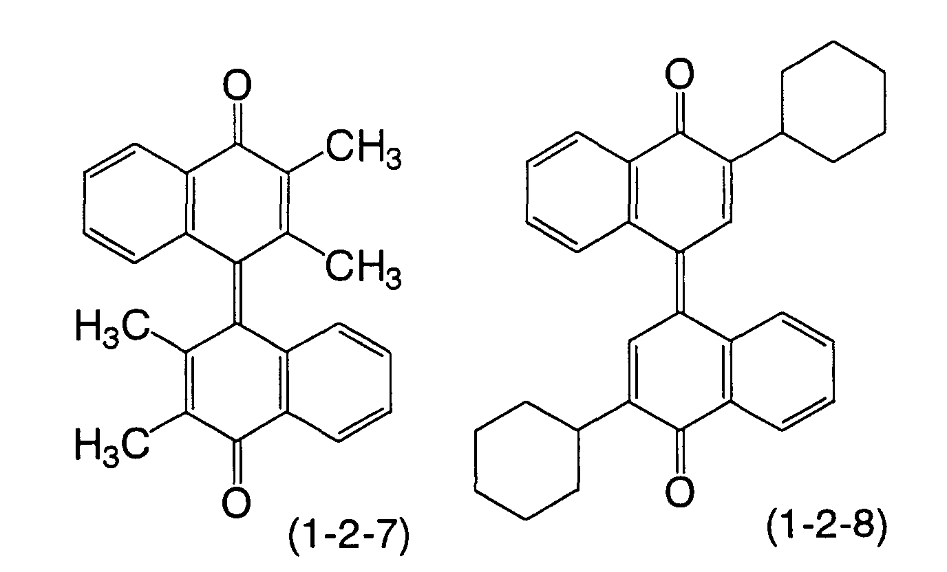
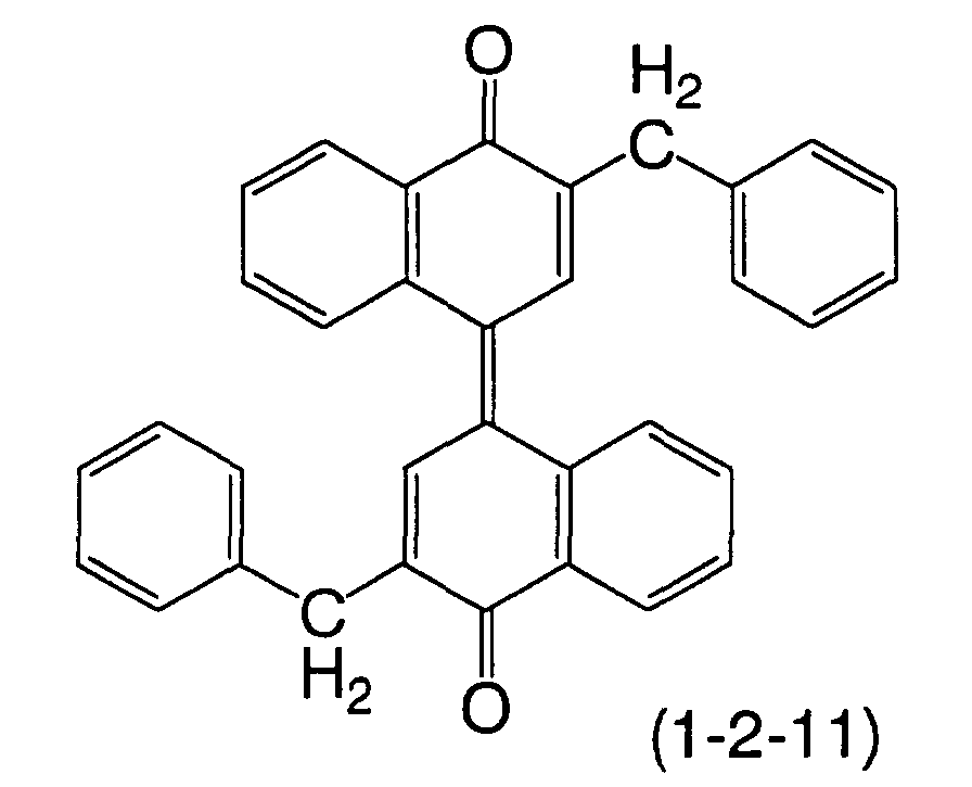
  • dinaphthoquinone compound of the formula (1-2) include compounds represented by formulas (1-2-1) to (1-2-11).
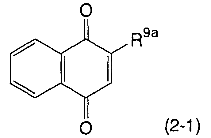
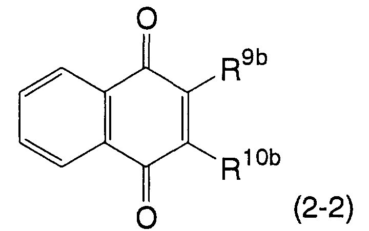
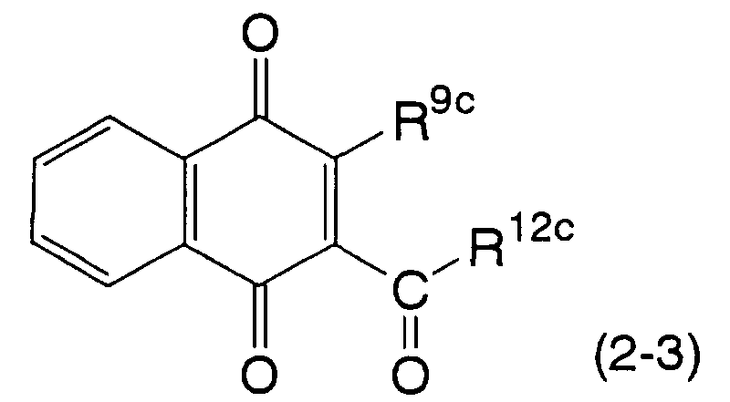
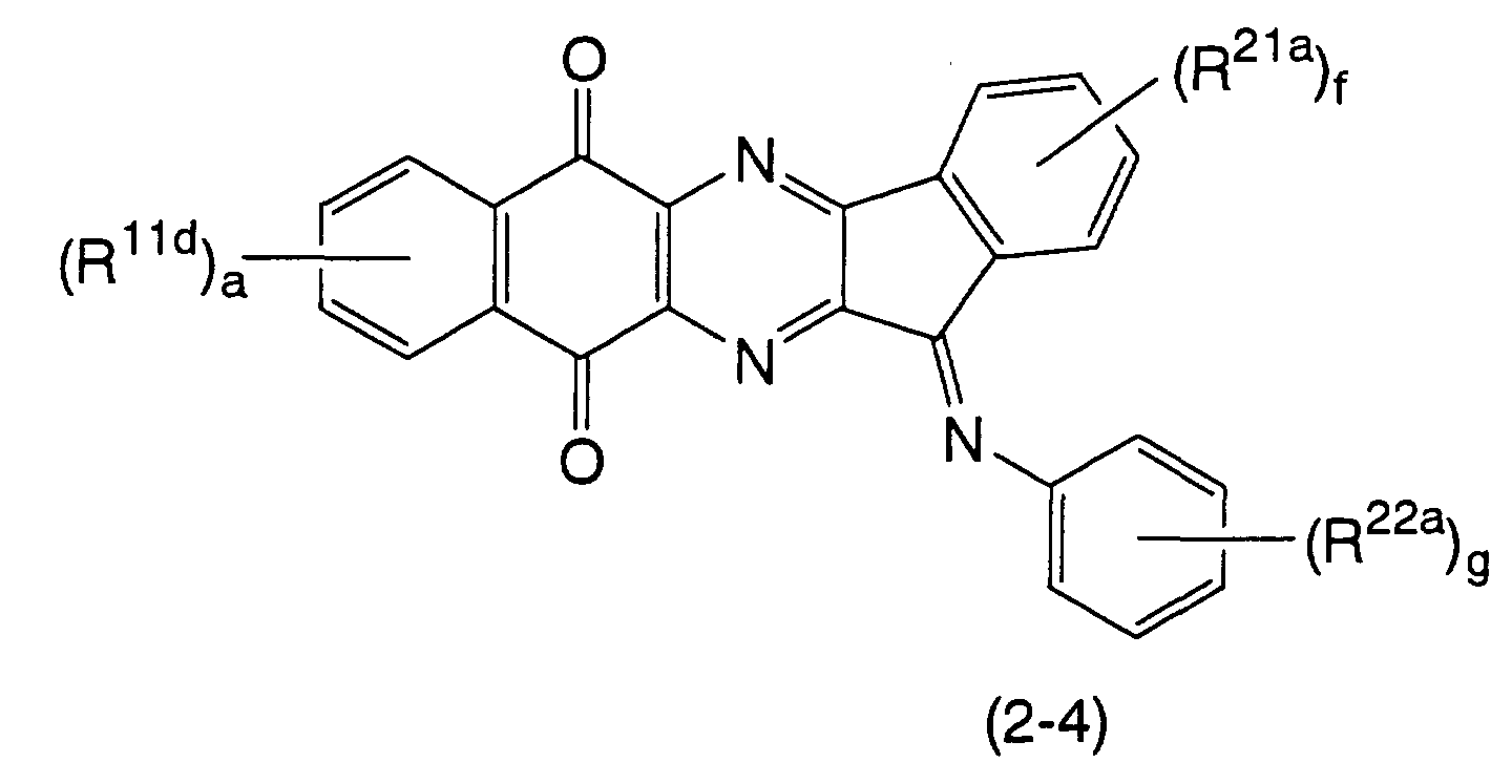
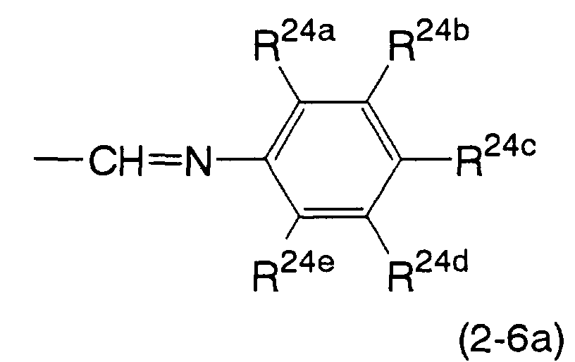
  • An example of a preferred naphthoquinone derivative of the formula (2) includes at least one selected from the group consisting of a naphthoquinone compound represented by a formula (2-1): wherein R 9a denotes an alkyl group, cycloalkyl group or aryl group; a naphthoquinone compound represented by a formula (2-2): wherein R 9b and R 10b are the same or different and each denoting an alkoxy group, alkylthio group, aryloxy group or arylthio group; a naphthoquinone compound represented by a formula (2-3): wherein R 9c denotes an alkyl group or aryl group; and R 12c denotes an alkyl group, alkoxy group, aryl group or aryloxy group; a diindenopyrazine compound represented by a formula (2-4): wherein R 11d , R 21a and R 22a are the same or different and each denoting a hydrogen
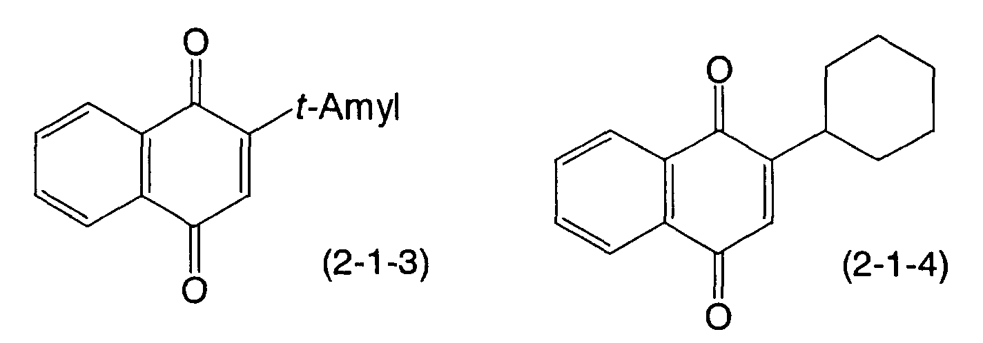
  • naphthoquinone compound of the formula (2-1) include compounds represented by formulas (2-1-1) to (2-1-6).
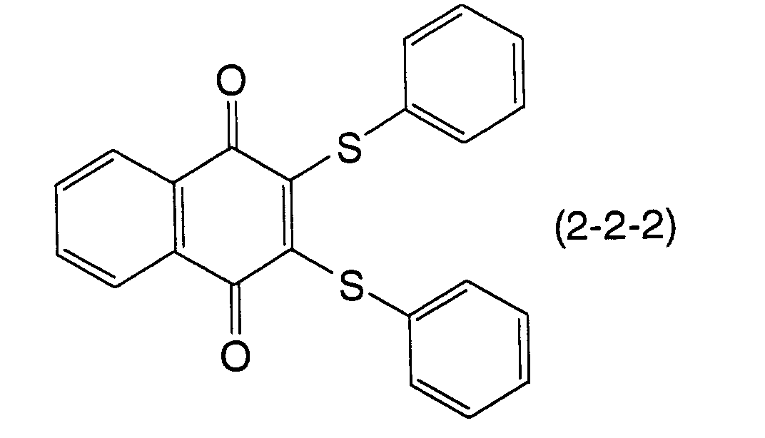
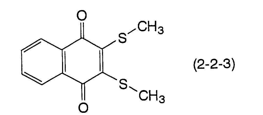
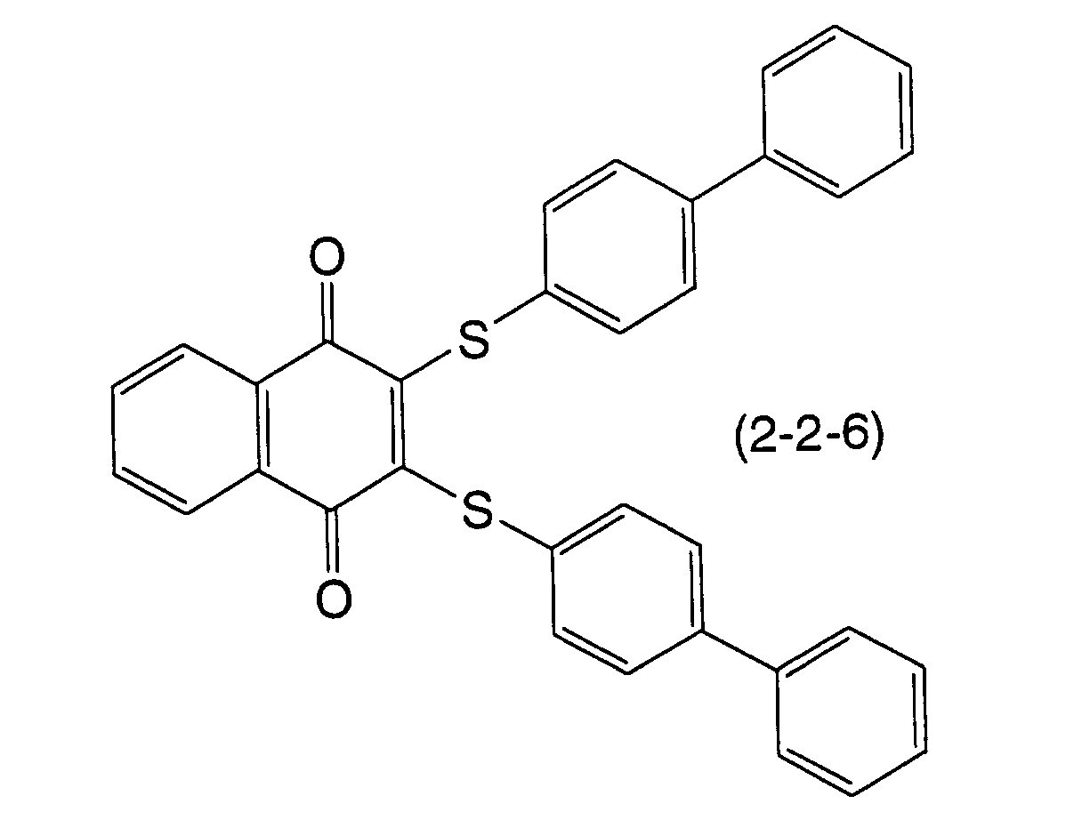
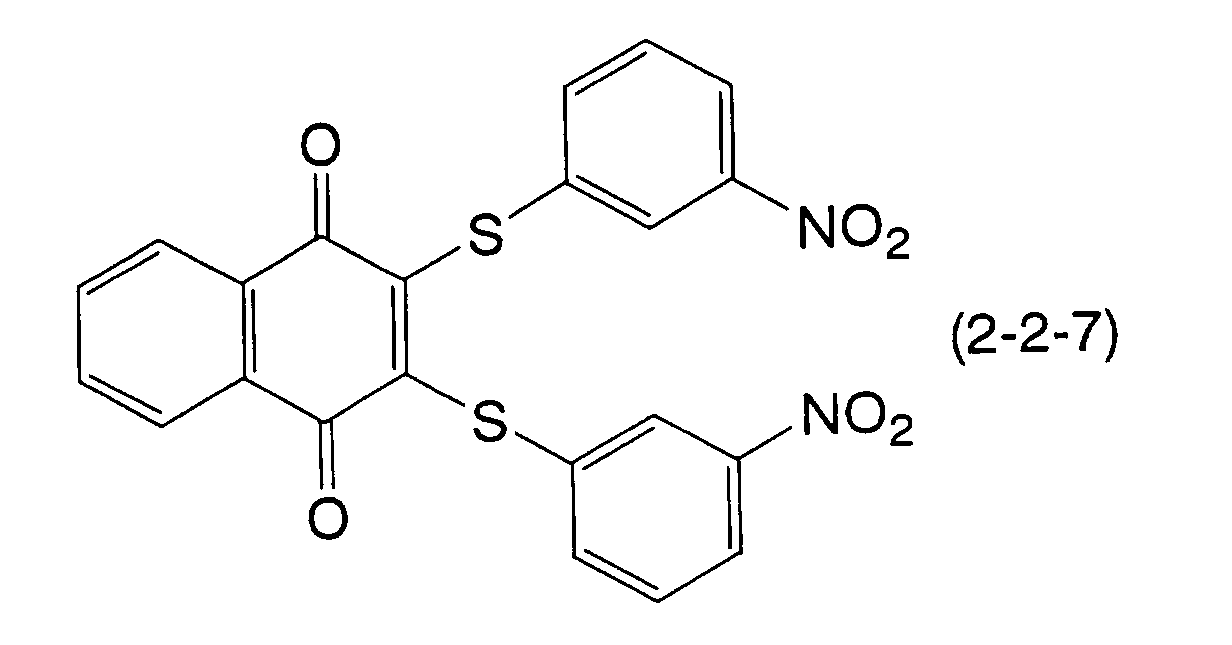
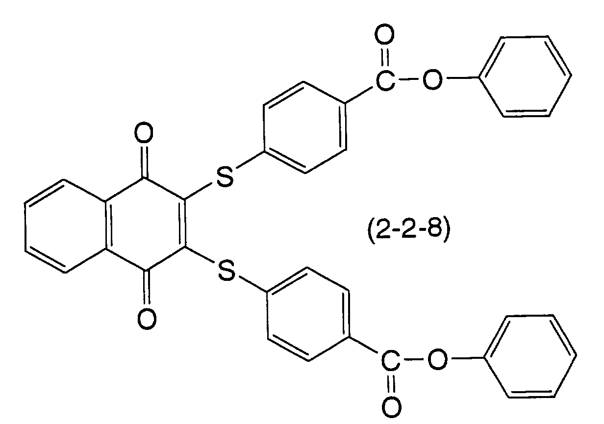
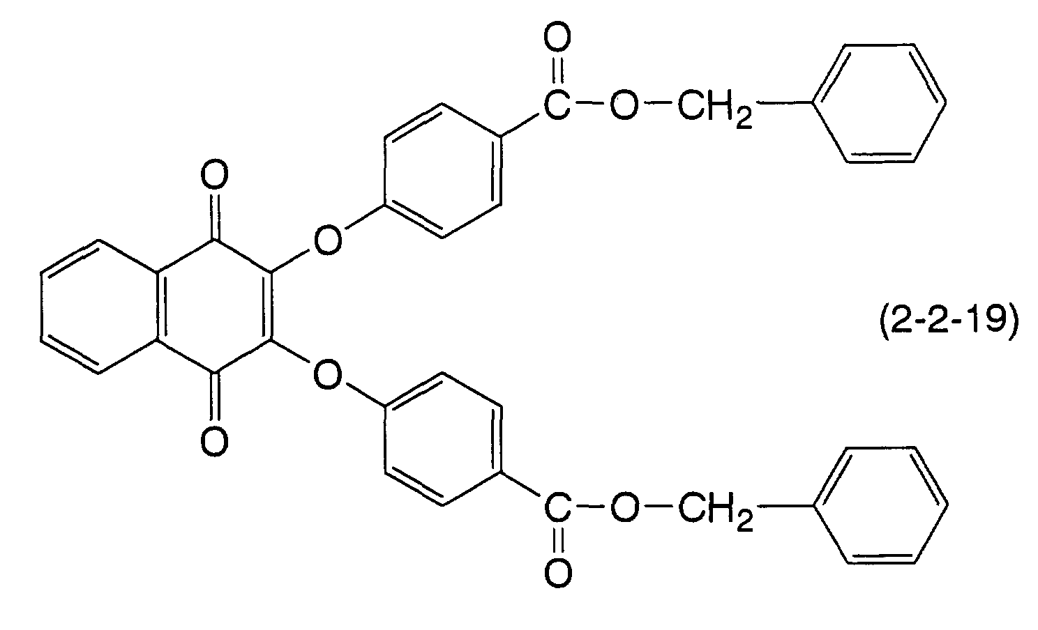
  • naphthoquinone compound of the formula (2-2) include compounds represented by formulas (2-2-1) to (2-2-23).
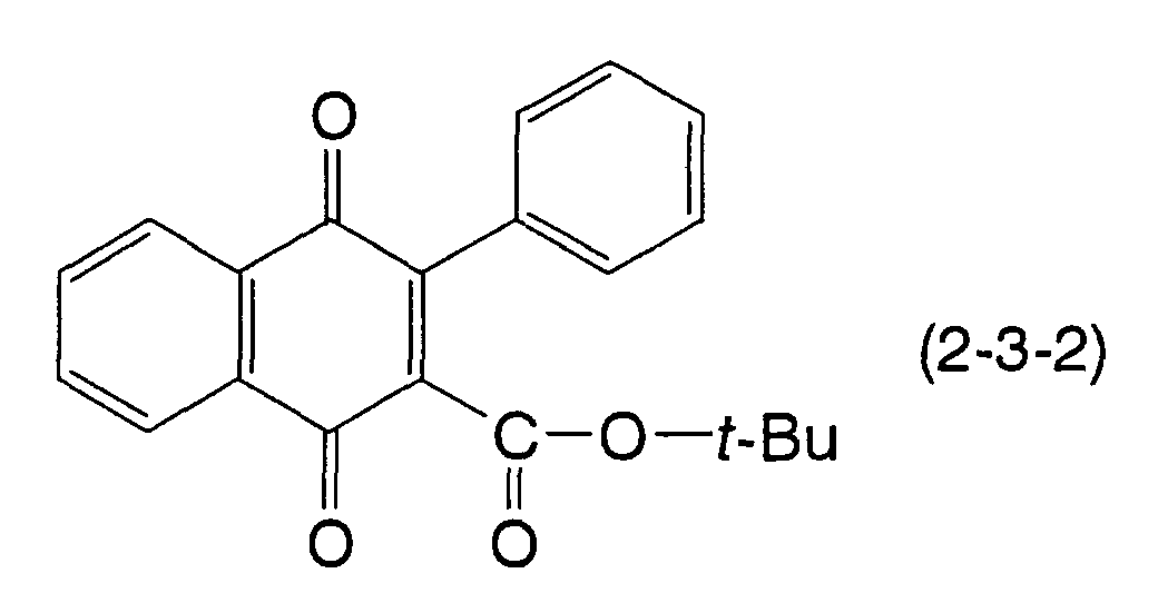
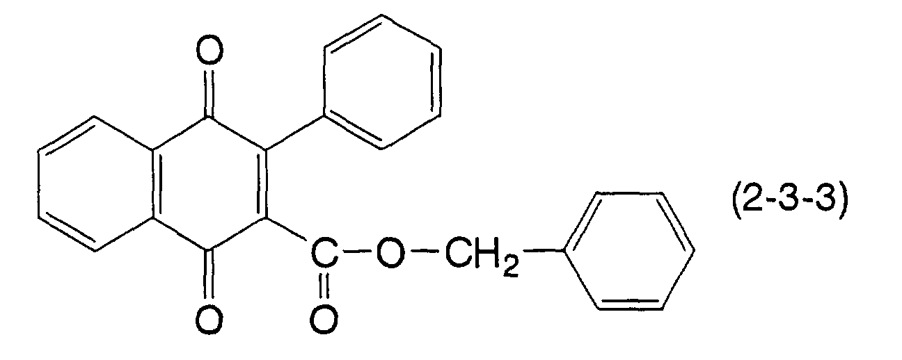
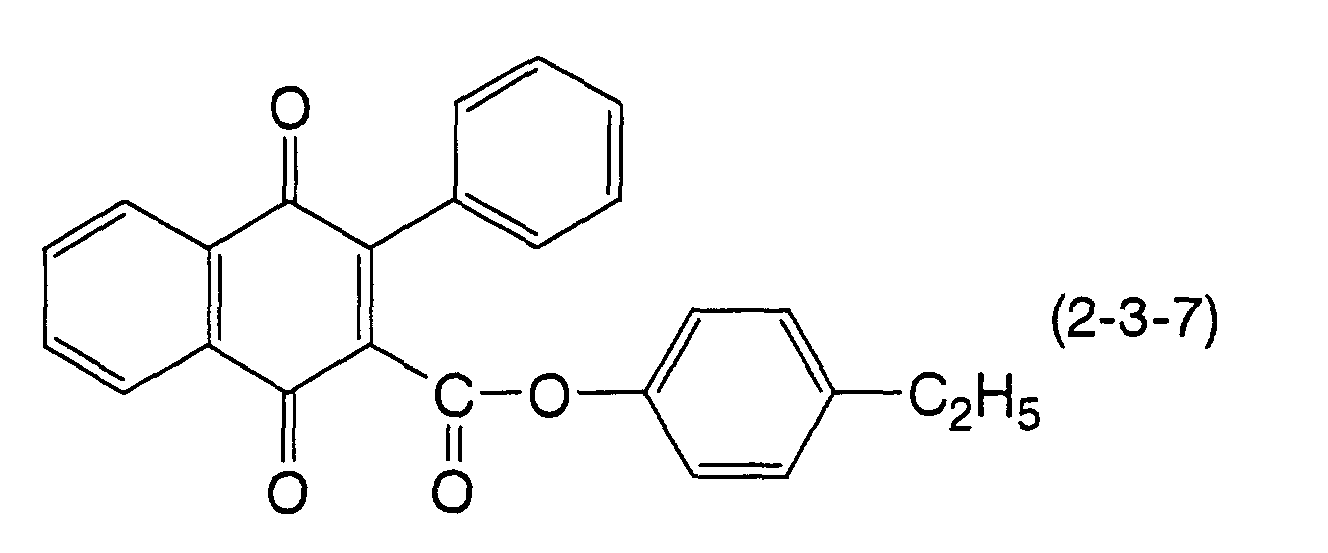
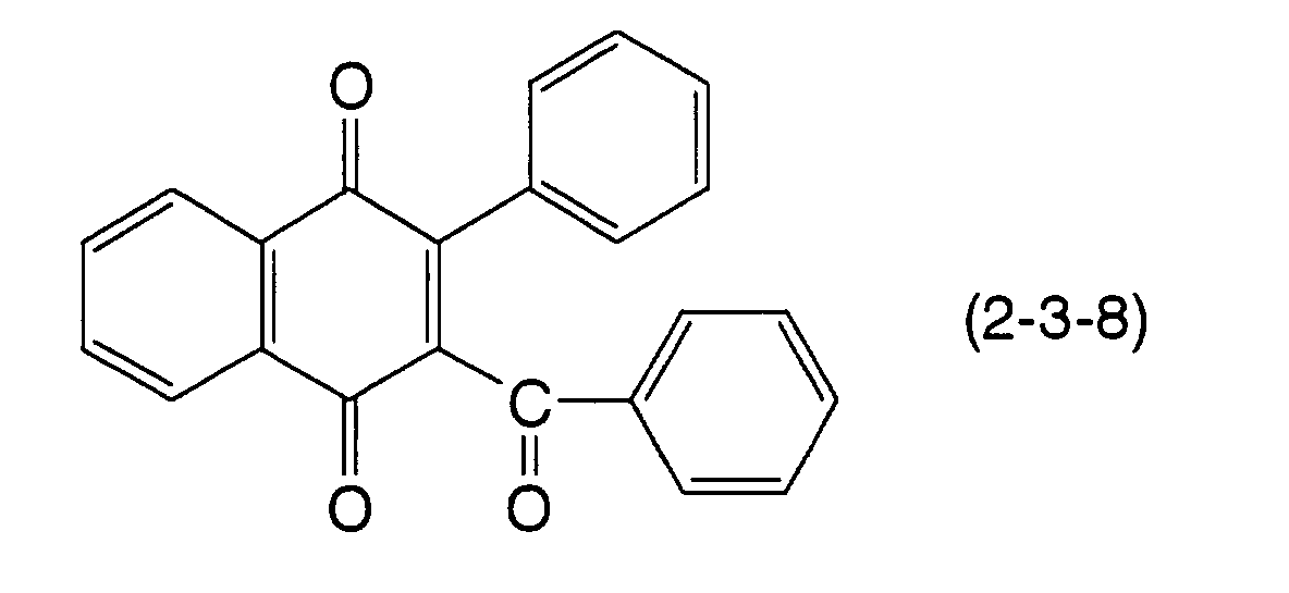
  • naphthoquinone compound of the formula (2-3) include compounds represented by formulas (2-3-1) to (2-3-11).
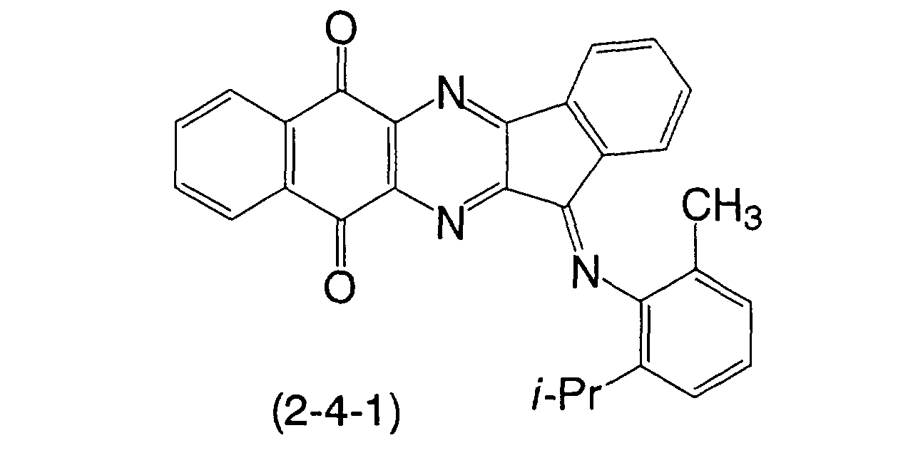
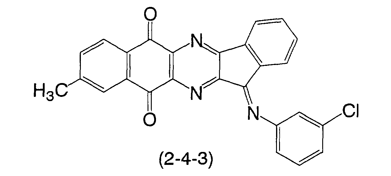
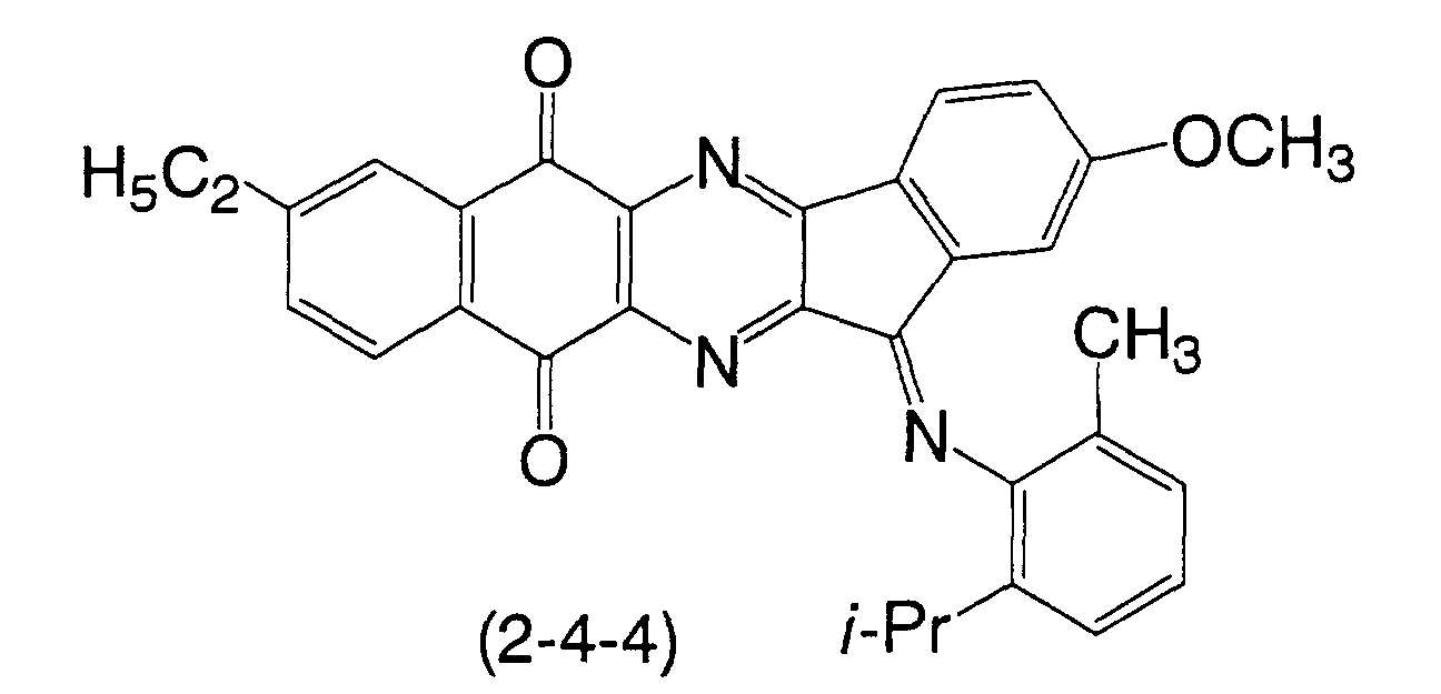
  • diindenopyrazine compound of the formula (2-4) include compounds represented by formulas (2-4-1) to (2-4-4).
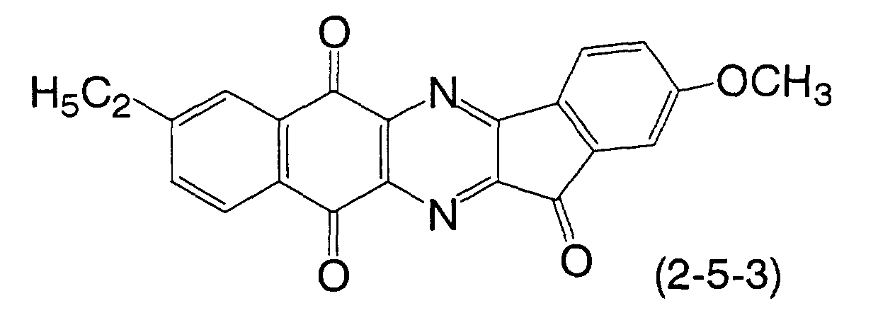
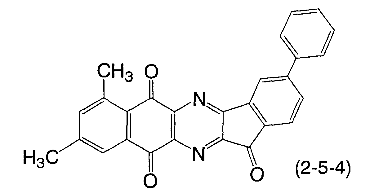
  • diindenopyrazine compound of the formula (2-5) include compounds represented by formulas (2-5-1) to (2-5-4).
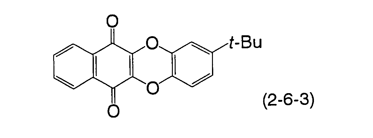
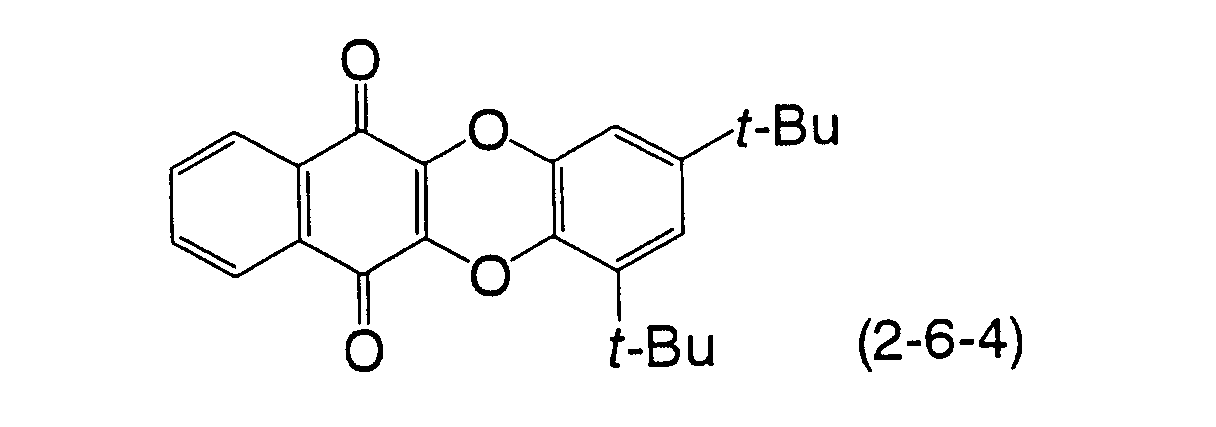
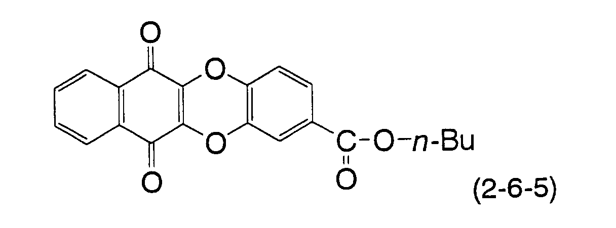
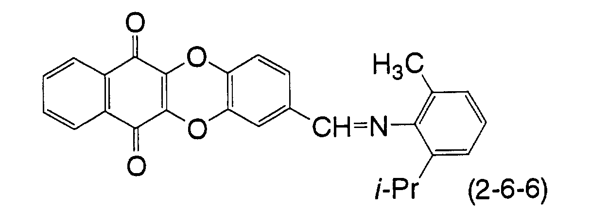
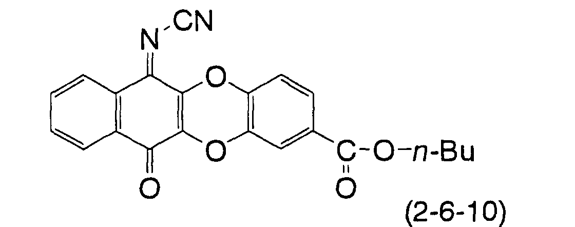
  • dioxotetracenedione compound of the formula (2-6) include compounds represented by formulas (2-6-1) to (2-6-11).
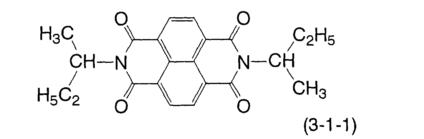
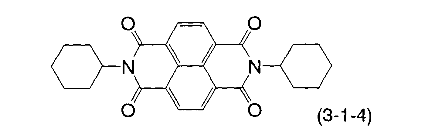
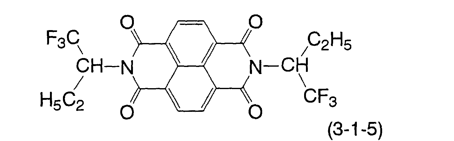
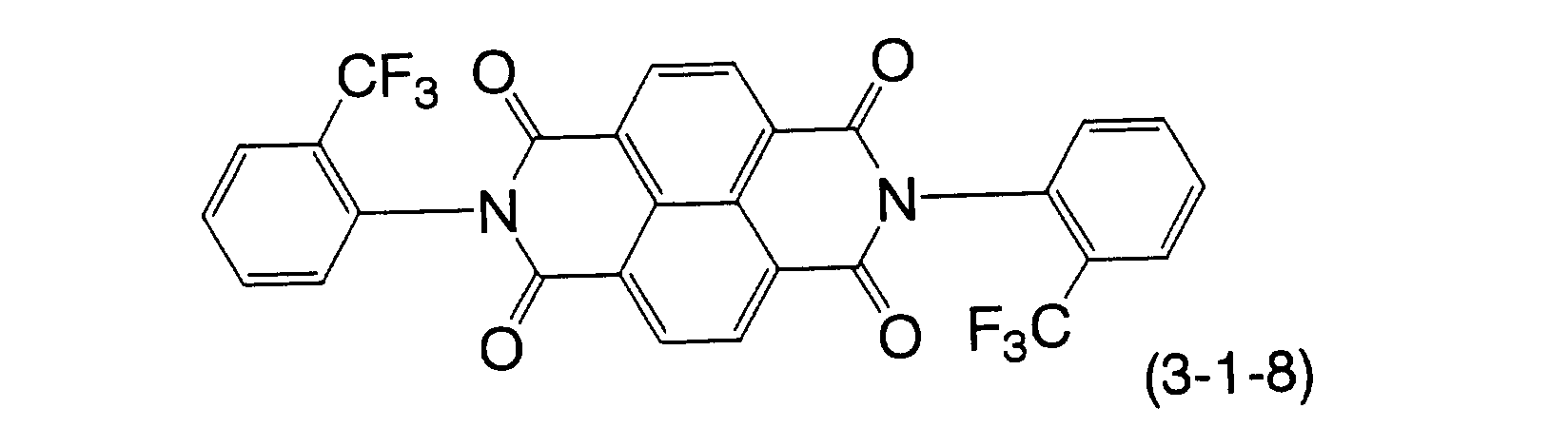
  • naphthylene diimide derivative of the formula (3) include compounds represented by formulas (3-1-1) to (3-1-13).
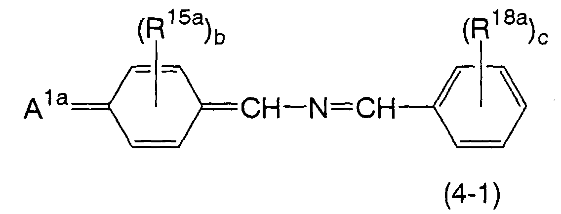
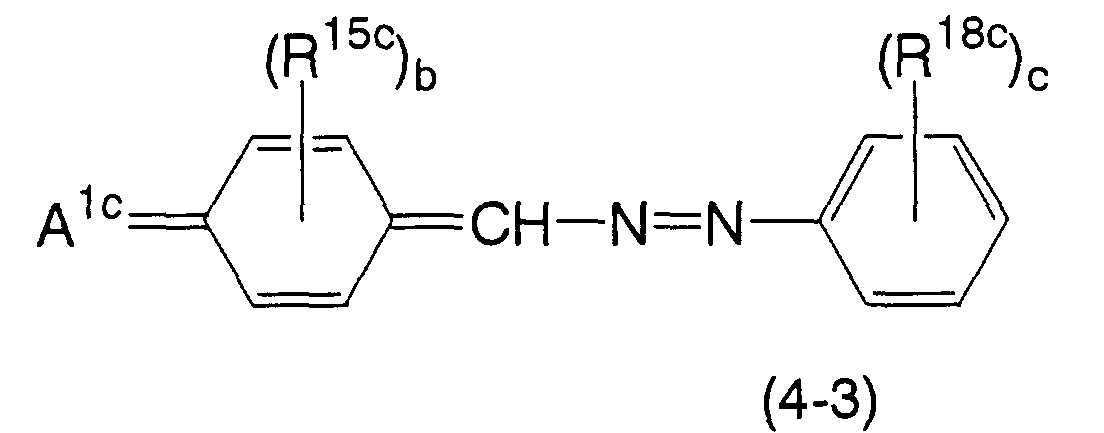
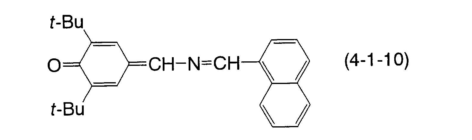
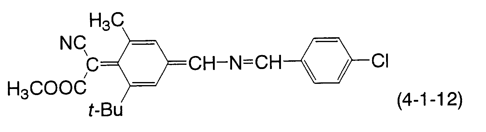
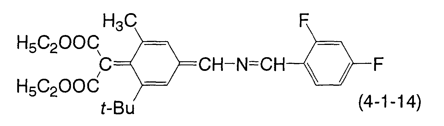
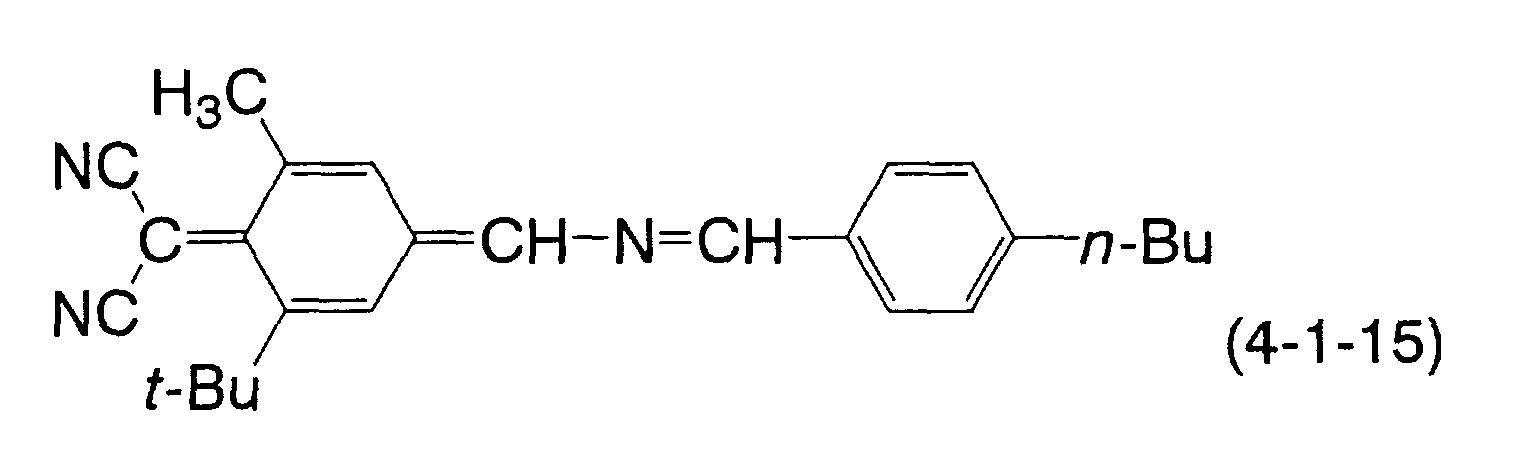
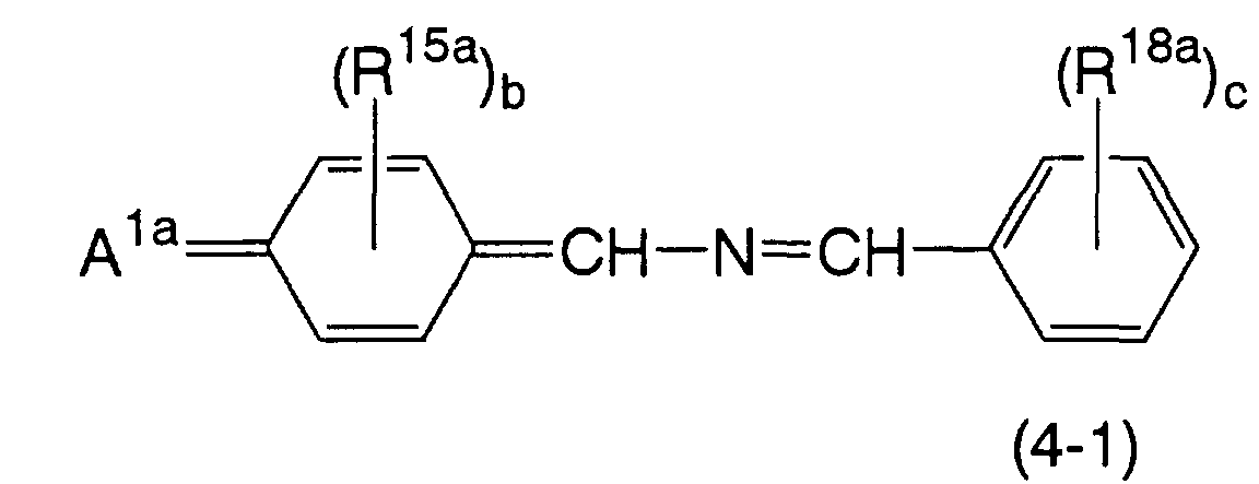
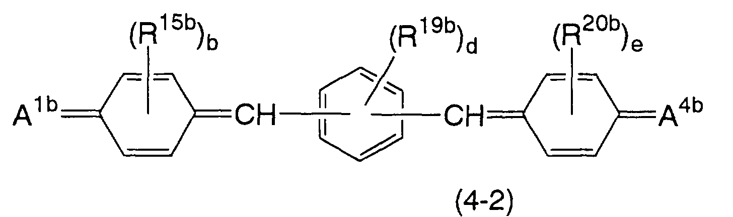
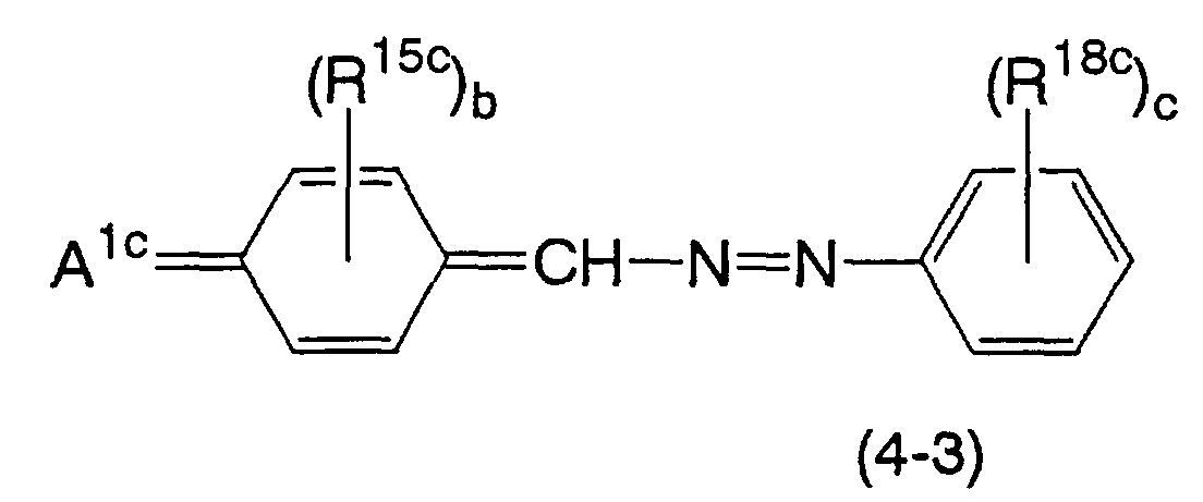
  • An example of a preferred quinone derivative of the formula (4) includes at least one selected from the group consisting of a compound represented by a formula (4-1): wherein R 15a and R 18a are the same or different and each denoting a hydrogen atom, halogen atom, alkyl group, alkoxy group, aryl group or aralkyl group; 'b' denotes an integer of 0 to 4, provided that when 'b' is 2 or more, the two groups R 15a bonded to adjacent carbon atoms of the ring may be linked together to form a condensed ring jointly with the ring; 'c' denotes an integer of 0 to 5, provided that when 'c' is 2 or more, the groups R 18a may be linked together to form a condensed ring jointly with the ring; and A 1a denotes an oxygen atom or the group represented by the formula (4a); a compound represented by a formula (4-2): wherein R 15b , R 19b and R 20b are the same
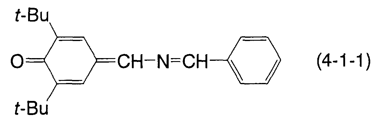
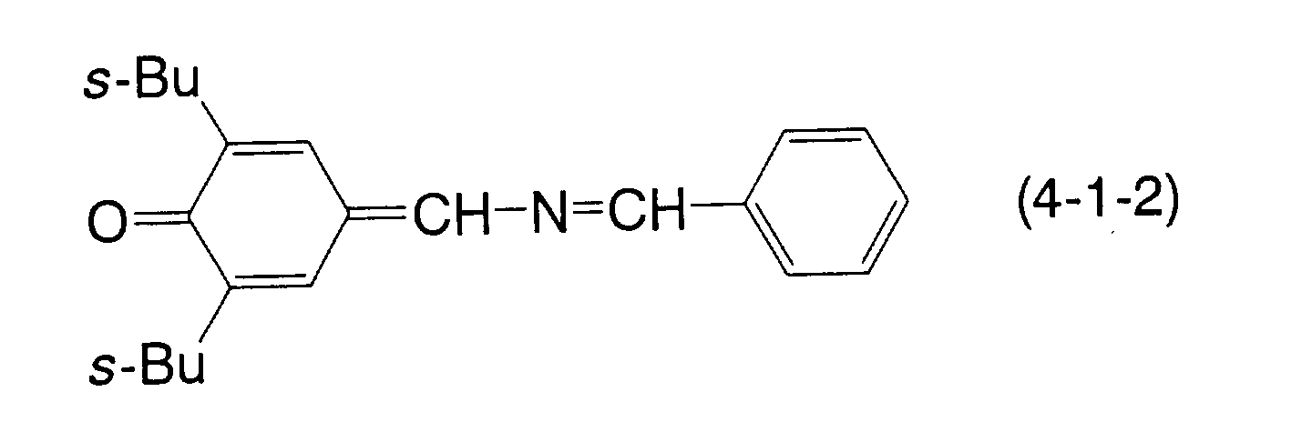
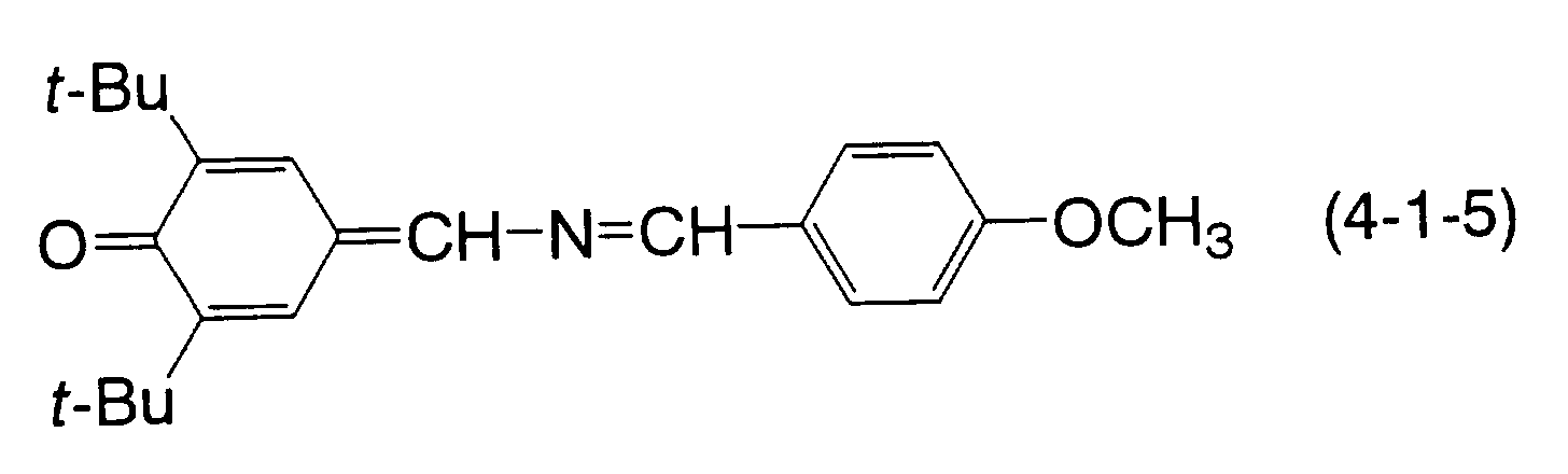
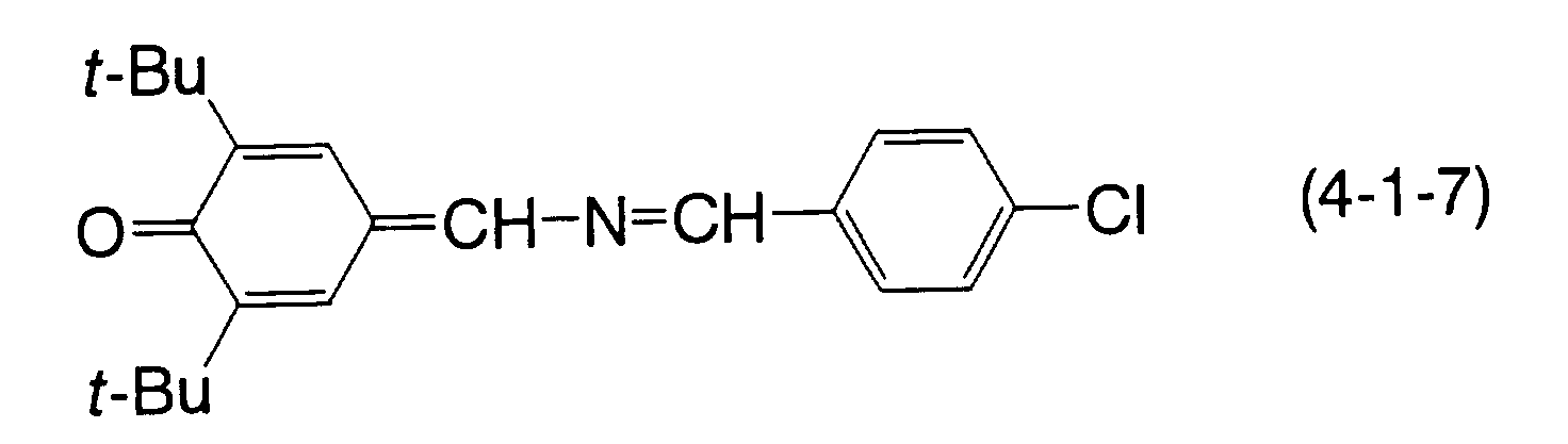
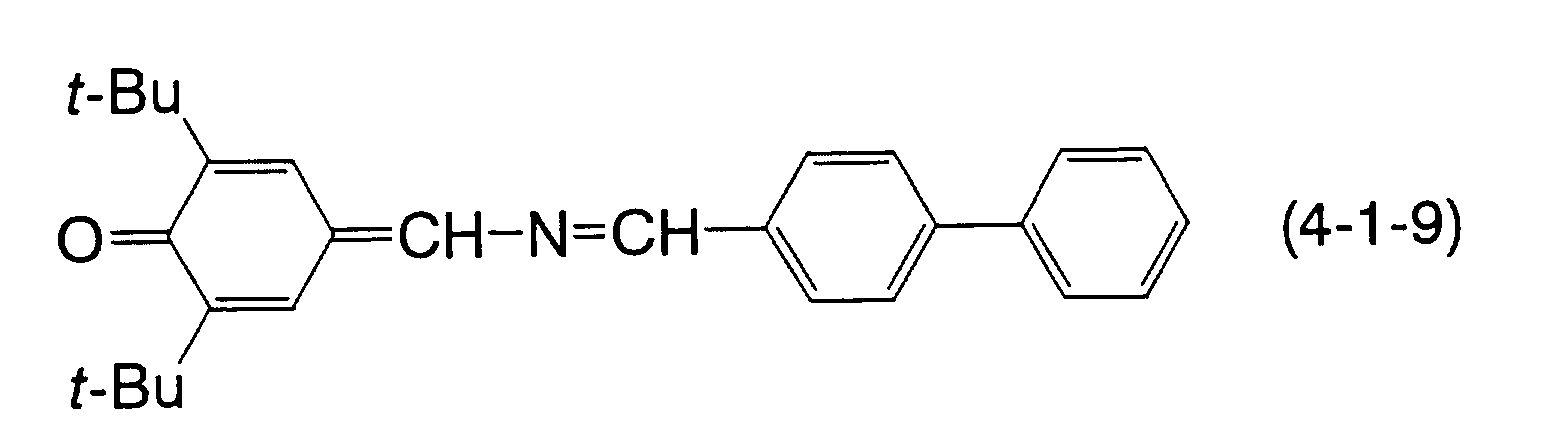
  • Specific examples of the compound of the formula (4-1) include compounds represented by formulas (4-1-1) to (4-1-16).
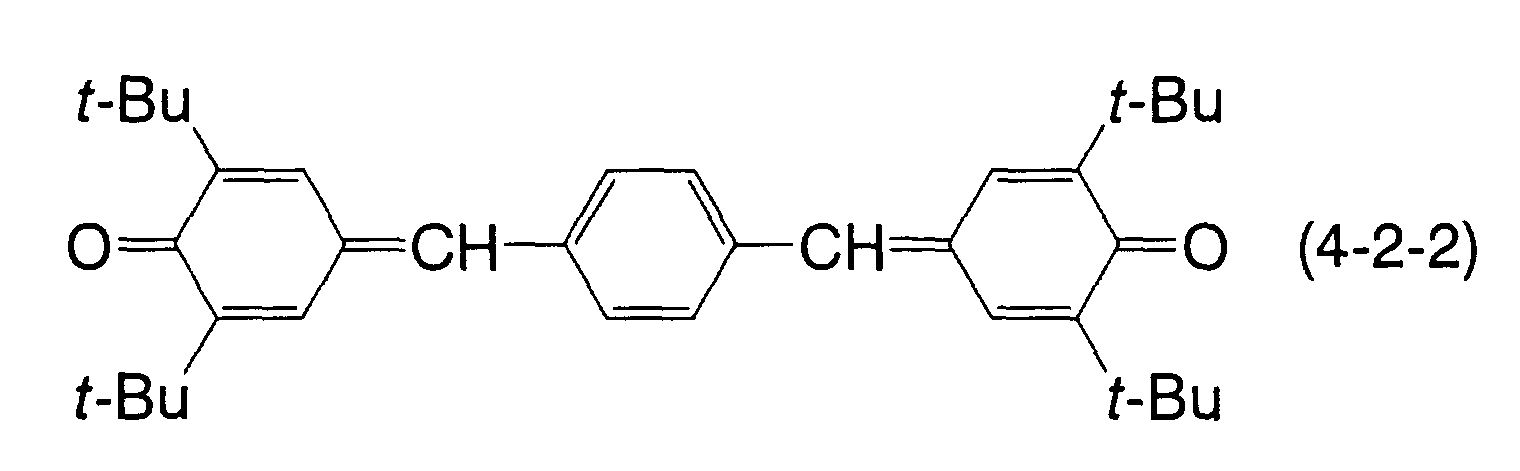
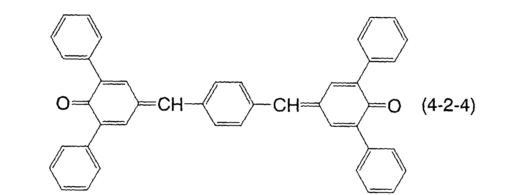
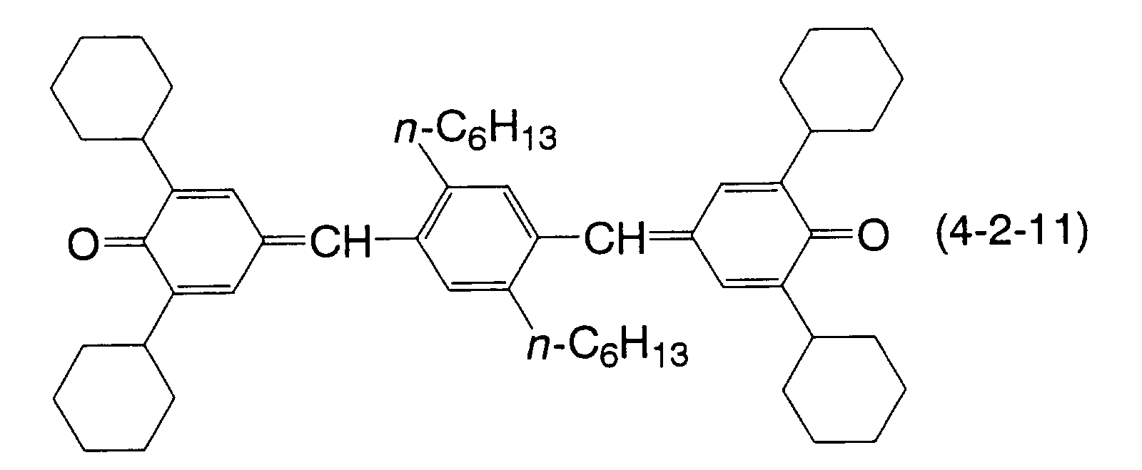
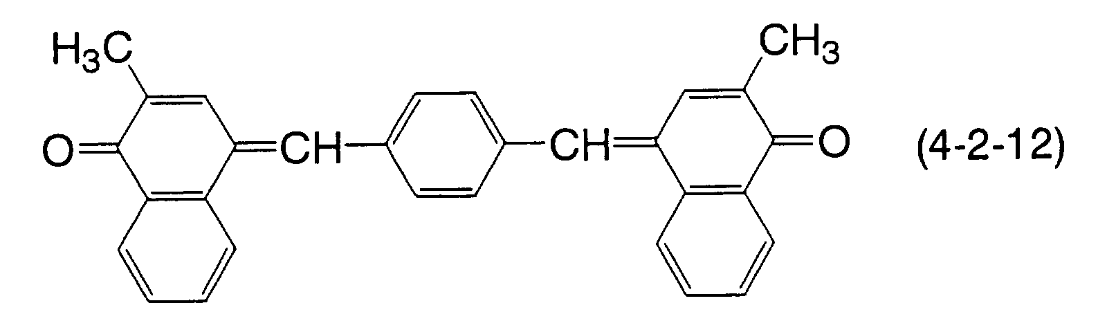
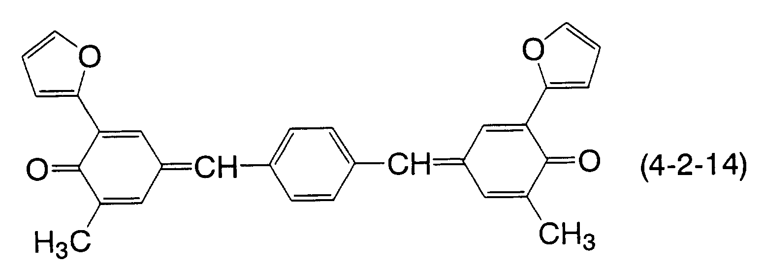
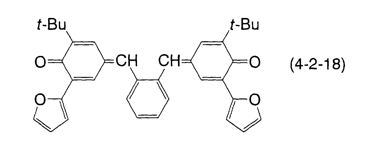
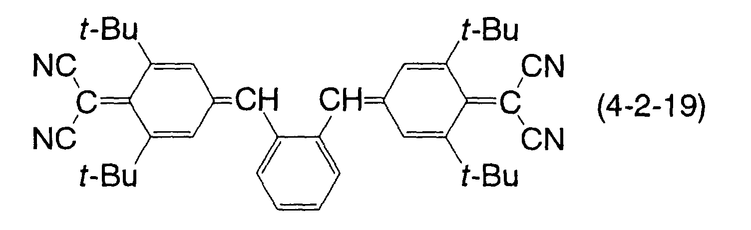
  • Specific examples of the compound of the formula (4-2) include compounds represented by formulas (4-2-1) to (4-2-20).
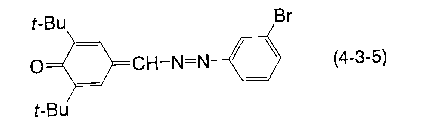
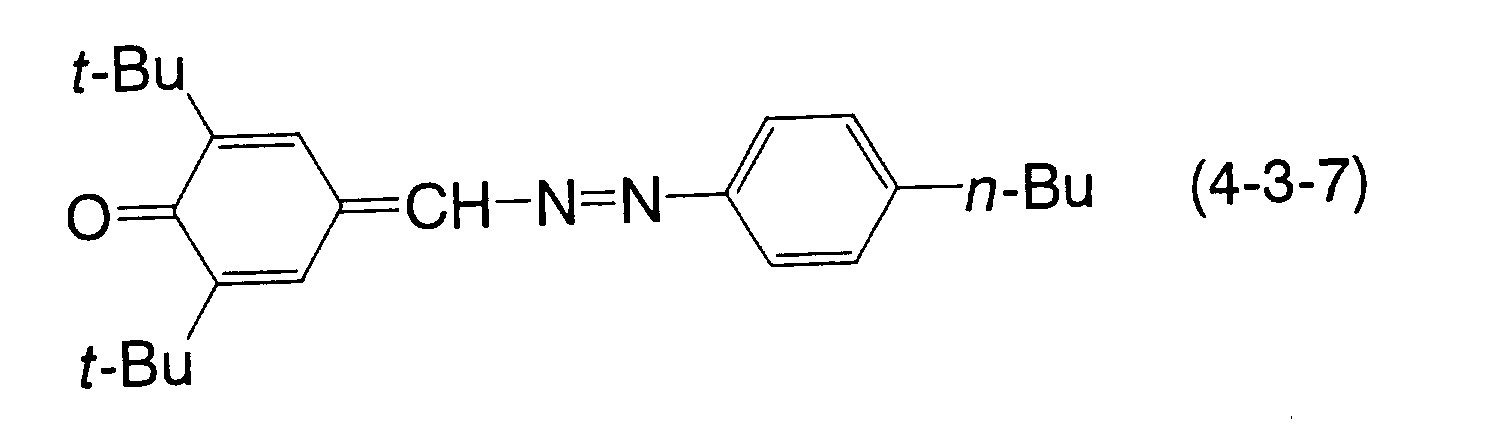
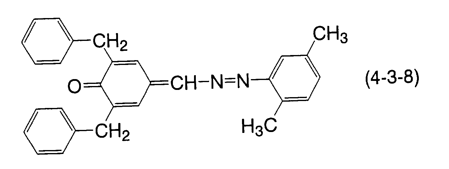
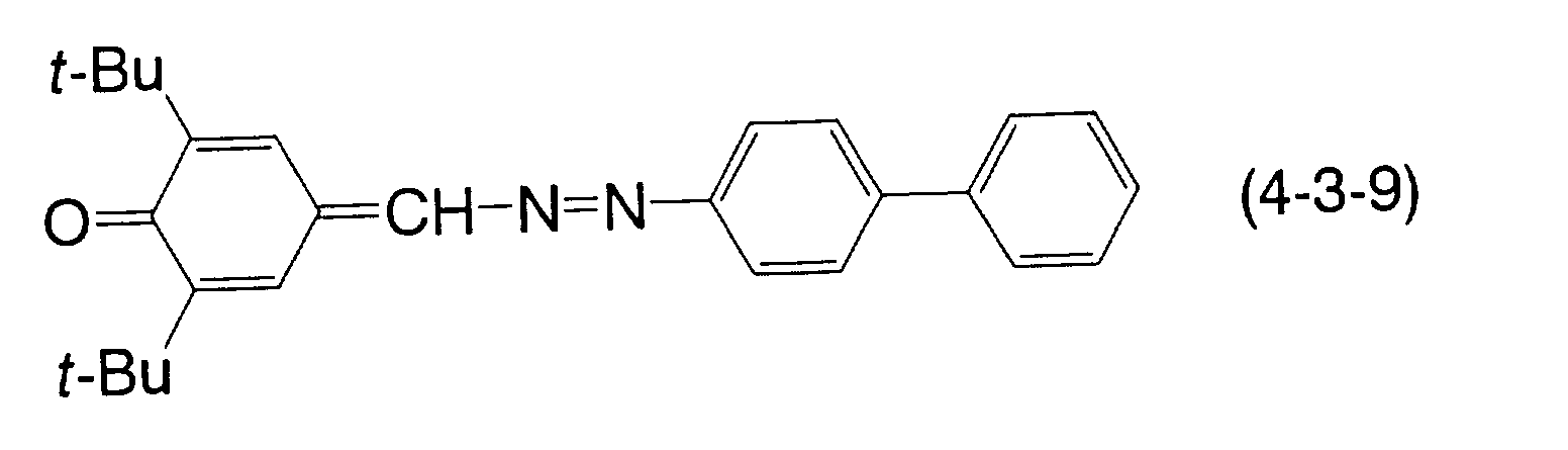
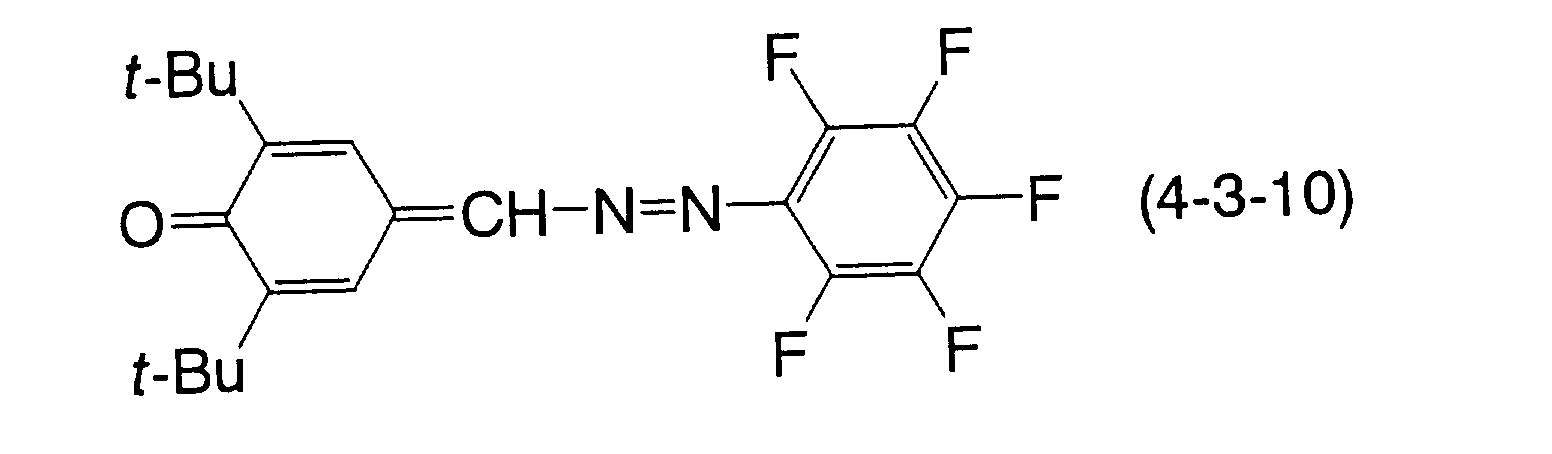
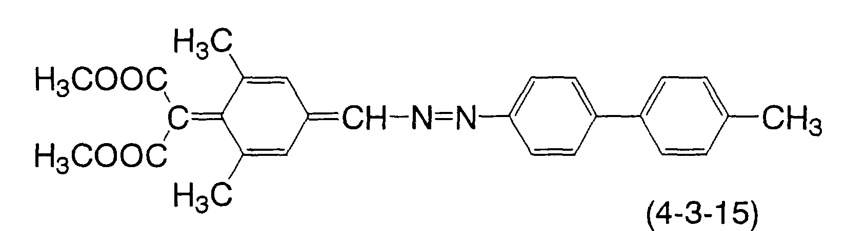
  • Specific examples of the compound of the formula (4-3) include compounds represented by formulas (4-3-1) to (4-3-15).
  • the organic photosensitive layer includes a single layer type and a multi-layer type, and the invention may be applicable to both of the types.
  • the single-layer photosensitive layer is formed by the steps of applying a coating solution to a conductive substrate and drying the solution, the coating solution prepared by dissolving or dispersing in a suitable organic solvent, at least one of the compounds of the formulas (1) to (4), the charge generating material, the charge transport material and the binder resin.
  • the single-layer photosensitive layer features a simple layer construction and good productivity.
  • the charge transport material may be dispensed with. However, it is preferred to admix the charge transport material in order to attain preferable sensitivity characteristics.
  • either of the positive-hole transport material and the electron-transport material may be used according to a charge polarity of the photosensitive layer.
  • both polarities charge transport materials may be used in combination with the above charge transport material.
  • a photosensitive layer including such charge transport materials of opposite polarities is advantageous in that a single layer construction is positively and negatively chargeable.
  • the multi-layer photosensitive layer is formed by the steps of overlaying on the conductive substrate the charge generating layer containing the charge generating material, applying a coating solution containing the charge transport material and the binder resin onto the resultant charge generating layer, and drying the solution thereby forming the charge transport layer. Otherwise, the multi-layer photosensitive layer may also be obtained by forming the charge transport layer over the conductive substrate, followed by forming thereover the charge generating layer.
  • the charge generating layer may further contain a charge transport material of the opposite polarity to that of the charge transport layer.
  • multi-layer photosensitive layer include the following four types:
  • the negative-charge photosensitive layers (a) and (b) are generally more preferred because of more excellent electrical characteristics thereof such as photosensitivity and residual potential.
  • the charge generating layer has quite a small thickness as compared with the charge transport layer and hence, the construction (a) with the charge transport layer laid on the upper side is more preferred.
  • the upper layer located at the outermost part of the above multi-layer photosensitive layer and contacting the surface protective layer is required to contain at least one of the compounds of the formulas (1) to (4).
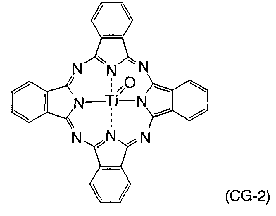
  • Examples of a usable charge generating material include powders of inorganic photoconductive materials such as selenium, selenium-tellurium, selenium-arsenic, cadmium sulfide, ⁇ -silicon and the like; and a variety of known pigments including phthalocyanine pigments comprising crystalline phthalocyanine compounds of various crystalline forms such as metal-free phthalocyanine represented by a formula (CG-1): titanyl phthalocyanine represented by a formula (CG-2): azo pigments, bisazo pigments, perylene pigments, anthanthrone pigments, indigo pigments, triphenylmethane pigments, threne pigments, toluidine pigments, pyrazoline pigments, quinacridone pigments, dithioketopyrolopyrrole pigments and the like.
  • CG-1 metal-free phthalocyanine represented by a formula (CG-1): titanyl phthalocyanine represented by a formula (CG
  • the charge generating materials may be used alone or in combination of two or more types such that the photosensitive layer may have sensitivity at a desired wavelength range.
  • a electrophotosensitive material having photosensitivity in the wavelength range of 700 nm or more is required by digital-optical image forming apparatuses such as laser beam printers, plain paper facsimiles and the like which utilize infrared light such as semiconductor laser beam. Accordingly, phthalocyanine pigments among the above exemplary compounds are preferably employed as the charge generating material.
  • Any of the various known electron-transporting compounds may be used as the electron transport material.
  • a preferred electron transport material include electron-attracting compounds which include, for example, benzoquinone compounds, diphenoquinone compounds, isatin compounds such as a compound represented by a formula (ET-1): naphthoquinone compounds, malononitrile, thiopyran compounds, tetracyanoethylene, 2,4,8-trinitrilothioxanthone, fluorenone compounds such as 2,4,7-trinitrilo-9-fluorenone, dinitrobenzene, dinitroanthracene, dinitroacridine, nitroanthraquinone, succinic anhydride, maleic anhydride, dibromomaleic anhydride, 2,4,7-trinitrofluorenoneimine compounds, ethylated nitrofluorenoneimine compounds, tryptantrin compounds, tryptantrinimine compounds, azafluorenone compounds, dinitropyridoquinazoline compounds, thioxanthene compounds, 2-phenyl
  • any of the various known positive-hole transporting compounds may be used as the positive-hole transport material.
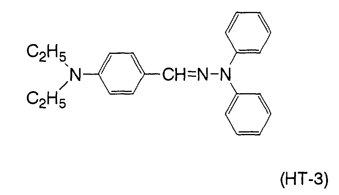
  • Examples of a particularly preferred positive-hole transport material include benzidine compounds, phenylenediamine compounds, naphthylenediamine compounds, phenantolylenediamine compounds, oxadiazole compounds such as 2,5-di(4-methylaminophenyl)-1,3,4-oxadiazole, styryl compounds such as 9-(4-diethylaminostyryl)anthracene, carbazole compounds such as poly-N-vinylcarbazole having a repeated unit represented by a formula (HT-1): organic polysilane compounds having a repeated unit represented by a formula (HT-2): [wherein R a and R b are the same or different each denoting an alkyl group, alkoxy group, aryl group or aralkyl group], pyrazoline compounds such as 1-phenyl-3-(p-dimethylaminophenyl)pyrazoline, hydrazone compounds such as diethylaminobenzaldehy
  • thermoplastic resins such as styrene polymers, styrene-butadiene copolymers, styrene-acrylonitrile copolymers, styrene-maleic acid copolymers, acrylic polymers, styrene-acryl copolymers, polyethylene, ethylene-vinyl acetate copolymers, chlorinated polyethylene, polyvinyl chloride, polypropylene, copolymers of vinyl chloride and vinyl acetate, polyester, alkyd resins, polyamide, polyurethane, polycarbonate, polyarylate, polysulfone, diarylphthalate resins, ketone resins, polyvinylbutyral resins, polyether resins and the like; crosslinking thermosetting resins such as silicone resins, epoxy resins, phenol resins, urea resins, melamine resins and the like; and photosetting resins such as epoxy-acrylate, urethane-acrylate
  • These resins may be used alone or in combination of two or more types.
  • the aforesaid high-molecular positive-hole transport material such as poly-N-vinylcarbazole or organic polysilane compound
  • such a compound also serves as the binder resin and hence, the aforesaid binder resin may be dispensed with.
  • the photosensitive layer may further contain any of the various additives such as fluorene compound, ultraviolet absorber, plasticizer, surfactant, leveling agent and the like.
  • a sensitizer such as terphenyl, halonaphthoquinone, acenaphthylene or the like.
  • the single-layer photosensitive layer may preferably contain 0.1 to 50 parts by weight or particularly 0.5 to 30 parts by weight of charge generating material, and 5 to 100 parts by weight or particularly 10 to 80 parts by weight of at least one of the compounds of the formulas (1) to (4), based on 100 parts by weight of binder resin.
  • the mixing ratio of the charge transport material may be suitably defined based on the charge polarity or construction of the photosensitive layer.
  • the mixing ratio of the positive-hole transport material is preferably in the range of 5 to 500 parts by weight or particularly of 25 to 200 parts by weight based on 100 parts by weight of binder resin. It is also possible to employ the aforesaid positive-hole transport material also serving as the binder resin so as to dispense with the binder resin.
  • the mixing ratio of the electron transport material is preferably in the range of 5 to 100 parts by weight or particularly of 10 to 80 parts by weight based on 100 parts by weight of binder resin.
  • positive-hole transport material and the electron transport material are used in combination as the charge transport material, for instance, these materials may preferably be present in total amount of 20 to 500 parts by weight or particularly of 30 to 200 parts by weight based on 100 parts by weight of binder resin.
  • the single-layer photosensitive layer may preferably have a thickness of 5 to 100 ⁇ m or particularly of 10 to 50 ⁇ m.
  • the charge generating layer disposed on the lower side thereof may be formed from the charge generating material alone or from the binder resin in which the charge generating material and, as required, the electron transport material are dispersed.
  • the charge generating material is present in the range of 5 to 1000 parts by weight or particularly of 30 to 500 parts by weight based on 100 parts by weight of binder resin while the electron transport material is present in the range of 1 to 200 parts by weight or particularly of 5 to 100 parts by weight based on 100 parts by weight of binder resin.
  • the charge transport layer disposed on the upper side may preferably contain the positive-hole transport material in the range of 10 to 500 parts by weight or particularly of 25 to 200 parts by weight based on 100 parts by weight of binder resin, and at least one of the compounds of the formulas (1) to (4) in the range of 0.1 to 250 parts by weight or particularly of 0.5 to 150 parts by weight based on 100 parts by weight of binder resin.
  • the aforesaid positive-hole transport material also serving as the binder resin may be used so as to dispense with the binder resin.
  • the charge generating layer may preferably have a thickness of about 0.01 to 5 ⁇ m or particularly of about 0.1 to 3 ⁇ m, whereas the charge transport layer may preferably have a thickness of about 2 to 100 ⁇ m or particularly of about 5 to 50 ⁇ m.
  • An intermediate layer or barrier layer may be formed between the single-layer or the multi-layer organic photosensitive layer and the conductive substrate or between the charge generating layer and the charge transport layer of the multi-layer photosensitive layer, so long as such a layer does not decrease the characteristics of the electrophotosensitive material.
  • the charge generating material, charge transport material, binder resin and the like may be dispersed, by mixing, into an organic solvent using a roll mill, ball mill, attritor, paint shaker, ultrasonic disperser or the like, thereby to prepare a coating solution, which may be applied and dried by the known means.
  • Examples of a usable organic solvent include alcohols such as methanol, ethanol, isopropanol, butanol and the like;
  • the coating solution may further contain a surfactant, leveling agent or the like for increasing the dispersibility of the charge generating material and charge transport material, and the surface smoothness of the photosensitive layer.
  • the inorganic surface protective layer is exemplified by a variety of surface protective layers comprising at least one element selected from the group consisting of metallic elements (the elements on the left side of a line interconnecting boron (B) and astatine (At) in the long-form periodic table) and carbon, or an inorganic compound containing any of these elements.
  • the surface protective layer may be formed by any of the various known vapor deposition methods including the chemical vapor deposition methods such as plasma CVD, photo CVD and the like, and the physical vapor deposition methods such as sputtering, vacuum deposition, ion plating and the like.
  • These films may contain a fractional amount of hydrogen (H) for improved electrical characteristics of the surface protective layer.
  • a usable raw material gas for introduction of a constituent element of the surface protective layer include the molecules of the constituent elements, and compounds thereof such as oxides, hydrides, nitrides and halides thereof, the compounds capable of presenting a gaseous state under normal temperature and pressure conditions or of being readily gassified under film forming conditions.
  • these compounds may be diluted with a gas such as hydrogen gas (H 2 ), helium gas, argon gas, neon gas or the like.
  • raw material gas examples include:
  • the. introduction of the other constituent elements may employ compounds capable of presenting a gaseous state under normal temperature and pressure conditions or of being readily gassified under film forming conditions.
  • films which each comprise one or more than one metallic elements selected from the group consisting of, for example, gallium (Ga), indium (In) and the like of the 13-group elements; germanium (Ge), tin (Sn), lead (Pb) and the like of the 14-group elements; arsenic (As), antimony (Sb) and the like of the 15-group elements; and selenium (Se) and the like of the 16-group elements, or which each comprise an inorganic compound comprising any of the above metallic elements.
  • metallic elements selected from the group consisting of, for example, gallium (Ga), indium (In) and the like of the 13-group elements; germanium (Ge), tin (Sn), lead (Pb) and the like of the 14-group elements; arsenic (As), antimony (Sb) and the like of the 15-group elements; and selenium (Se) and the like of the 16-group elements, or which each comprise an inorganic compound comprising any of the above metallic elements
  • Preferred as the inorganic surface protective layer are, for example, the carbon (C) film, silicon-carbon (SiC) composite film and the like.
  • the thickness of the inorganic surface protective layer may preferably be in the range of 0.01 to 30 ⁇ m or particularly of 0.1 to 10 ⁇ m.
  • the inorganic film defining the surface protective layer may be in any of the amorphous form, microcrystalline form, and crystalline form. Further, the film may comprise a mixture of amorphous and crystalline particles.
  • the conductive substrate may employ substrates formed from various materials having conductivity.
  • a usable conductive substrate include those formed from metals such as iron, aluminum, copper, tin, platinum, silver, vanadium, molybdenum, chromium, cadmium, titanium, nickel, palladium, indium, stainless steel, brass and the like; those formed from a plastic material on which any of the above metals is deposited or laminated; and glass substrate coated with aluminum iodide, tin oxide, indium oxide or the like.
  • the substrate itself may have the conductivity or the surface thereof may have the conductivity. It is preferred that the conductive substrate has a sufficient mechanical strength in use.
  • the conductive substrate may have any form, such as sheet, drum and the like, according to the construction of the image forming apparatus to which the conductive substrate is applied.
  • CG-1 charge generating material represented by the formula (CG-1)
  • 100 parts by weight of poly-N-vinylcarbazole (number-average molecular weight Mn 9500) serving as the positive-hole transport material and the binder resin and having the repeated unit represented by the formula (HT-1)
  • the resultant coating solution was dip coated on an aluminum tube as the conductive substrate and then was air dried at 100°C for 30 minutes.
  • a single-layer photosensitive layer having a thickness of 25 ⁇ m.
  • the aluminum tube formed with the single-layer photosensitive layer was placed in a chamber of a plasma CVD system.
  • the air within the chamber was evacuated to reach a degree of vacuum of 0.67 Pa while a heater of the system was operated to adjust the temperature of the tube to 50°C.
  • methane gas (CH 4 ), silane gas (SiH 4 ) and hydrogen gas (H 2 ) were fed into the chamber at respective flow rates listed below, thereby to adjust the degree of vacuum to 0.47 hPa.
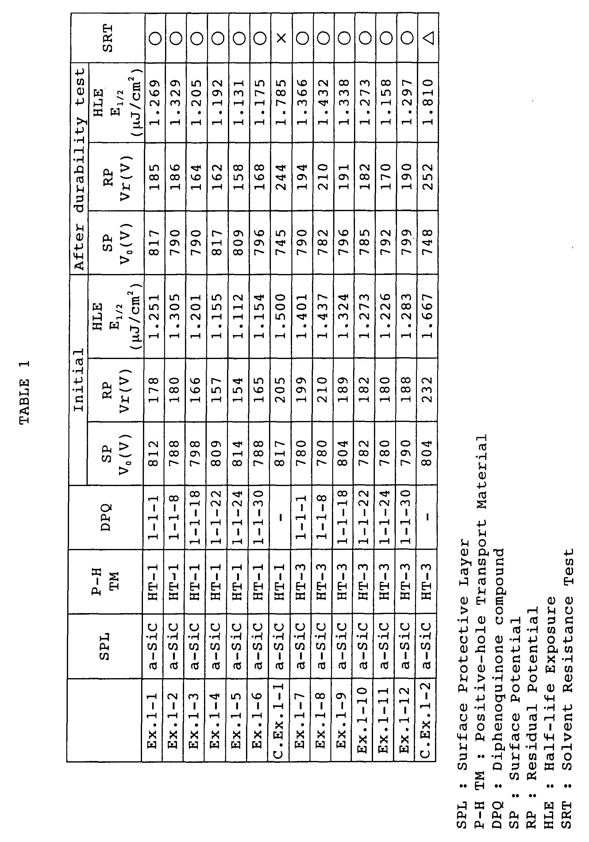
  • Electrophotosensitive materials of Examples 1-2 to 1-6 were fabricated the same way as in Example 1-1, except that each of the examples used 40 parts by weight of diphenoquinone compound of the formula of a number listed in Table 1.
  • An electrophotosensitive material of Comparative Example 1-1 was fabricated the same way as in Example 1-1, except that the diphenoquinone compound was dispensed with.
  • Each of the electrophotosensitive materials of the above examples and comparative examples was charged at +800 ⁇ 20V and the surface potential V 0 (V) thereof was measured using a drum sensitivity tester available from GENTEC Co.
  • a bandpass filter was used to extract monochromatic light from white light from a halogen lamp as a light source of the tester, the monochromatic light having a wavelength of 780 nm and a half width of 20 nm.
  • the surface of the above electrophotosensitive material was irradiated with the monochromatic light at a light intensity of 10 ⁇ W/cm 2 for 1.0 second while the half-life exposure E 1/2 ( ⁇ J/cm 2 ) was determined by measuring the time elapsed before the surface potential V 0 (V) decreased to half.
  • the residual potential V r (V) was determined by measuring a surface potential after a lapse of 0.5 seconds from the start of the light exposure.
  • the electrophotosensitive materials of the above examples and comparative examples were each mounted in the drum sensitivity tester available from GENTEC Co.
  • the surface of each electrophotosensitive material was charged and exposed to light under the same conditions as in the photosensitivity test (I) and then was exposed to light (wavelength of 660 nm) from an erase lamp of the tester for static elimination.
  • the process of charging, light exposure and static elimination was consecutively repeated in 2,000 cycles with a rotational speed of the electrophotosensitive material set to 40 rpm. Subsequent to the process repeated in cycles, the electrophotosensitive material was subjected to the photosensitivity test (I) again for determining the surface potential V 0 (V), half-life exposure E 1/2 ( ⁇ J/cm 2 ) and residual potential V r (V).
  • the adhesion between the surface protective layer and the organic photosensitive layer was examined as follows. A pipette was used to apply methanol dropwise to the surface of each of the electrophotosensitive materials of the examples and comparative examples and changes of surface were visually observed. The solvent resistance of each electrophotosensitive material was evaluated based on the following criteria:
  • electrophotosensitive materials of these comparative examples were significantly decreased in photosensitivity when formed with the surface protective layer, because they presented, in the initial stage, large residual potentials after light exposure and large half-life exposures.
  • the electrophotosensitive materials of these comparative examples were found to have poor durability because they were significantly increased in residual potential and half-life exposure after the durability test.
  • Electrophotosensitive materials of Examples 1-13 to 1-24 and of Comparative Examples 1-3, 1-4 were fabricated the same way as in Examples 1-1 to 1-12 and Comparative Examples 1-1, 1-2, except that the following procedure was taken to form a surface protective layer of amorphous carbon (C) having a thickness of 0.5 ⁇ m, instead of the silicon-carbon composite film, over the surface of the single-layer photosensitive layer.
  • C amorphous carbon
  • the aluminum tube formed with the single-layer photosensitive layer was placed in the chamber of the plasma CVD system.
  • the air within the chamber was evacuated to reach a degree of vacuum of 0.67 Pa while the heater of the system was operated to adjust the temperature of the tube to 50°C.
  • methane gas (CH 4 ) and hydrogen gas (H 2 ) were fed into the chamber at respective flow rates listed below, thereby to adjust the degree of vacuum to 0.47 hPa.
  • a high-frequency electric field having a frequency of 13.56 MHz and an output of 200 W was applied for causing glow discharge in the chamber.
  • the plasma CVD process was performed for depositing a film of amorphous carbon (C) at a film growth rate of 0.15 ⁇ m/hr, thereby forming the surface protective layer of the aforesaid thickness over the surface of the single-layer photosensitive layer.
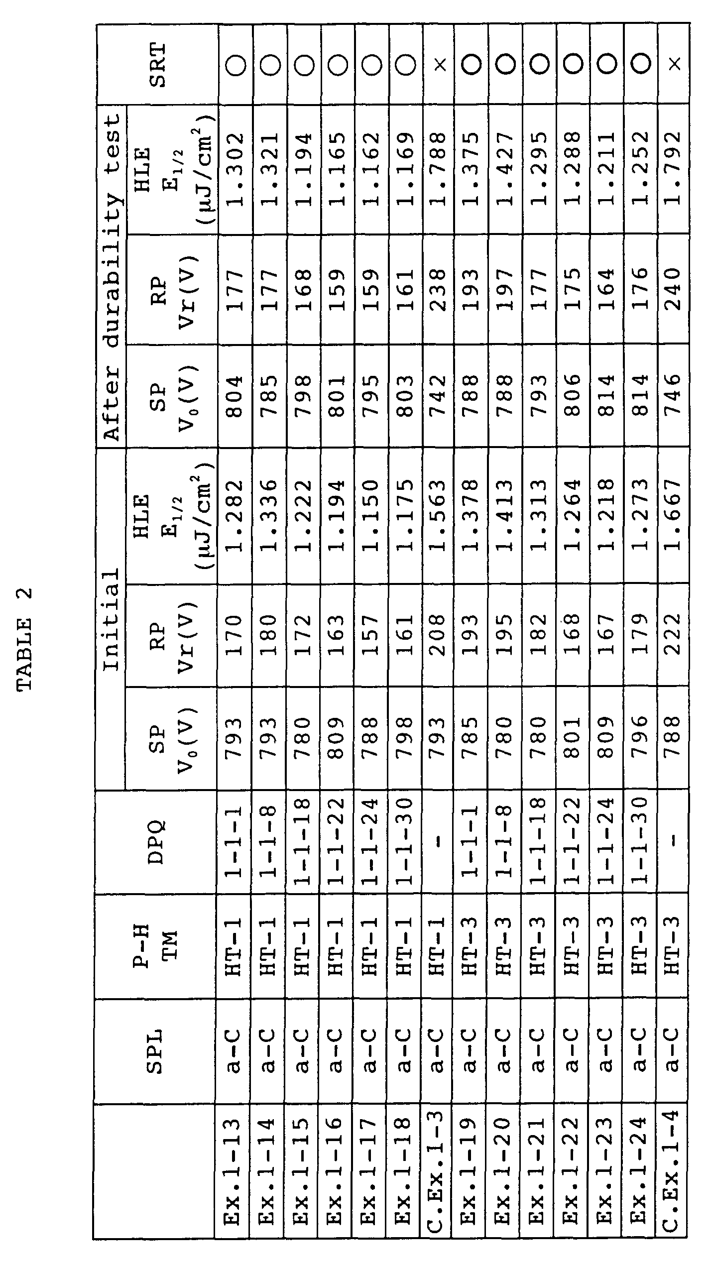
  • the electrophotosensitive materials of the above examples and comparative examples were subjected to the same photosensitivity test (I), durability test (I) and solvent resistance test as the above and evaluated for the characteristics thereof. The results are listed in Table 2.
  • electrophotosensitive materials of these comparative examples were significantly decreased in photosensitivity when formed with the surface protective layer, because they presented, in the initial stage, large residual potentials after light exposure and large half-life exposures.
  • the electrophotosensitive materials of these comparative examples were found to have poor durability because they were significantly increased in residual potential and half-life exposure after the durability test.
  • Electrophotosensitive materials of Examples 1-25, 1-26 and of Comparative Example 1-5 were fabricated the same way as in Examples 1-11, 1-12 and Comparative Examples 1-2, except that the following procedure was taken to form a surface protective layer of amorphous silicon-nitrogen (SiN) composite film having a thickness of 0.5 ⁇ m, instead of the silicon-carbon composite film, over the surface of the single-layer photosensitive layer.
  • SiN amorphous silicon-nitrogen
  • the aluminum tube formed with the single-layer photosensitive layer was placed in the chamber of the plasma CVD system.
  • the air within the chamber was evacuated to reach a degree of vacuum of 0.67 Pa while the heater of the system was operated to adjust the temperature of the tube to 50°C.
  • silane gas (SiH 4 ), nitrogen gas (N 2 ) and hydrogen gas (H 2 ) were fed into the chamber at respective flow rates listed below, thereby to adjust the degree of vacuum to 0.47 hPa.
  • a high-frequency electric field having a frequency of 13.56 MHz and an output of 150 W was applied for causing glow discharge in the chamber.
  • the plasma CVD process was performed for depositing a silicon-nitrogen (SiN) composite film at a film growth rate of 0.75 ⁇ m/hr, thereby forming the surface protective layer of the aforesaid thickness over the surface of the single-layer photosensitive layer.
  • Electrophotosensitive materials of Examples 1-27, 1-28 and of Comparative Example 1-6 were fabricated the same way as in Examples 1-11, 1-12 and Comparative Examples 1-2, except that the following procedure was taken to form a surface protective layer of amorphous carbon-nitrogen (CN) composite film having a thickness of 0.5 ⁇ m, instead of the silicon-carbon composite film, over the surface of the single-layer photosensitive layer.
  • CN amorphous carbon-nitrogen
  • the aluminum tube formed with the single-layer photosensitive layer was placed in the chamber of the plasma CVD system.
  • the air within the chamber was evacuated to reach a degree of vacuum of 0.67 Pa while the heater of the system was operated to adjust the temperature of the tube to 50°C.
  • methane gas (CH 4 ), nitrogen gas (N 2 ) and hydrogen gas (H 2 ) were fed into the chamber at respective flow rates listed below, thereby to adjust the degree of vacuum to 0.47 hPa.
  • a high-frequency electric field having a frequency of 13.56 MHz and an output of 150 W was applied for causing glow discharge in the chamber.
  • the plasma CVD process was performed for depositing a carbon-nitrogen (CN) composite film at a film growth rate of 0.10 ⁇ m/hr, thereby forming the surface protective layer of the aforesaid thickness over the surface of the single-layer photosensitive layer.
  • CN carbon-nitrogen
  • Electrophotosensitive materials of Examples 1-29, 1-30 and of Comparative Example 1-7 were fabricated the same way as in Examples 1-11, 1-12 and Comparative Examples 1-2, except that the following procedure was taken to form a surface protective layer of amorphous carbon-boron (CB) composite film having a thickness of 0.5 ⁇ m, instead of the silicon-carbon composite film, over the surface of the single-layer photosensitive layer.
  • CB amorphous carbon-boron
  • the aluminum tube formed with the single-layer photosensitive layer was placed in the chamber of the plasma CVD system.
  • the air within the chamber was evacuated to reach a degree of vacuum of 0.67 Pa while the heater of the system was operated to adjust the temperature of the tube to 50°C.
  • methane gas (CH 4 ), diborane gas (B 2 H 6 ) and hydrogen gas (H 2 ) were fed into the chamber at respective flow rates listed below, thereby to adjust the degree of vacuum to 0.47 hPa.
  • a high-frequency electric field having a frequency of 13.56 MHz and an output of 150 W was applied for causing glow discharge in the chamber.
  • the plasma CVD process was performed for depositing a carbon-boron (CB) composite film at a film growth rate of 0.10 ⁇ m/hr, thereby forming the surface protective layer of the aforesaid thickness over the surface of the single-layer photosensitive layer.
  • CB carbon-boron
  • Electrophotosensitive materials of Examples 1-31, 1-32 and of Comparative Example 1-8 were fabricated the same way as in Examples 1-11, 1-12 and Comparative Examples 1-2, except that the following procedure was taken to form a surface protective layer of amorphous carbon-fluorine (CF) composite film having a thickness of 0.5 ⁇ m, instead of the silicon-carbon composite film, over the surface of the single-layer photosensitive layer.
  • CF amorphous carbon-fluorine
  • the aluminum tube formed with the single-layer photosensitive layer was placed in the chamber of the plasma CVD system.
  • the air within the chamber was evacuated to reach a degree of vacuum of 0.67 Pa while the heater of the system was operated to adjust the temperature of the tube to 50°C.
  • methane gas (CH 4 ), carbon tetrafluoride gas (CF 4 ) and hydrogen gas (H 2 ) were fed into the chamber at respective flow rates listed below, thereby to adjust the degree of vacuum to 0.47 hPa.
  • a high-frequency electric field having a frequency of 13.56 MHz and an output of 150 W was applied for causing glow discharge in the chamber.
  • the plasma CVD process was performed for depositing a carbon-fluorine (CF) composite film at a film growth rate of 0.10 ⁇ m/hr, thereby forming the surface protective layer of the aforesaid thickness over the surface of the single-layer photosensitive layer.
  • CF carbon-fluorine
  • Electrophotosensitive materials of Examples 1-33, 1-34 and of Comparative Example 1-9 were fabricated the same way as in Examples 1-11, 1-12 and Comparative Examples 1-2, except that the following procedure was taken to form a surface protective layer of amorphous boron-nitrogen (BN) composite film having a thickness of 0.5 ⁇ m, instead of the silicon-carbon composite film, over the surface of the single-layer photosensitive layer.
  • BN amorphous boron-nitrogen
  • the aluminum tube formed with the single-layer photosensitive layer was placed in the chamber of the plasma CVD system.
  • the air within the chamber was evacuated to reach a degree of vacuum of 0.67 Pa while the heater of the system was operated to adjust the temperature of the tube to 50°C.
  • diborane gas (B 2 H 6 ), nitrogen gas (N 2 ) and hydrogen gas (H 2 ) were fed into the chamber at respective flow rates listed below, thereby to adjust the degree of vacuum to 0.47 hPa.
  • a high-frequency electric field having a frequency of 13.56 MHz and an output of 150 W was applied for causing glow discharge in the chamber.
  • the plasma CVD process was performed for depositing a boron-nitrogen (BN) composite film at a film growth rate of 0.08 ⁇ m/hr, thereby forming the surface protective layer of the aforesaid thickness over the surface of the single-layer photosensitive layer.
  • BN boron-nitrogen
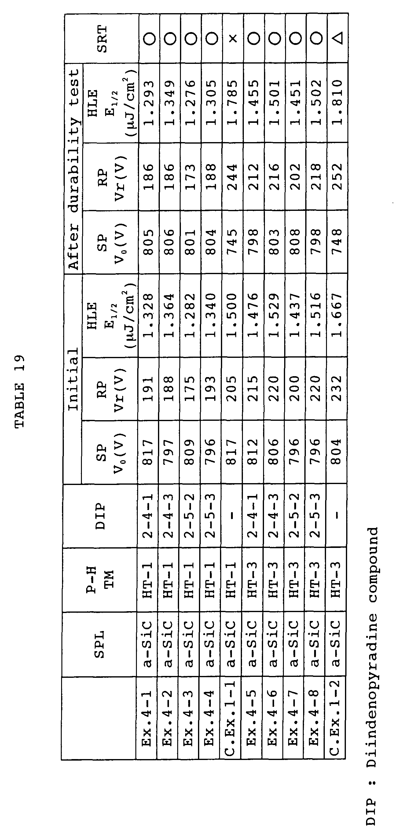
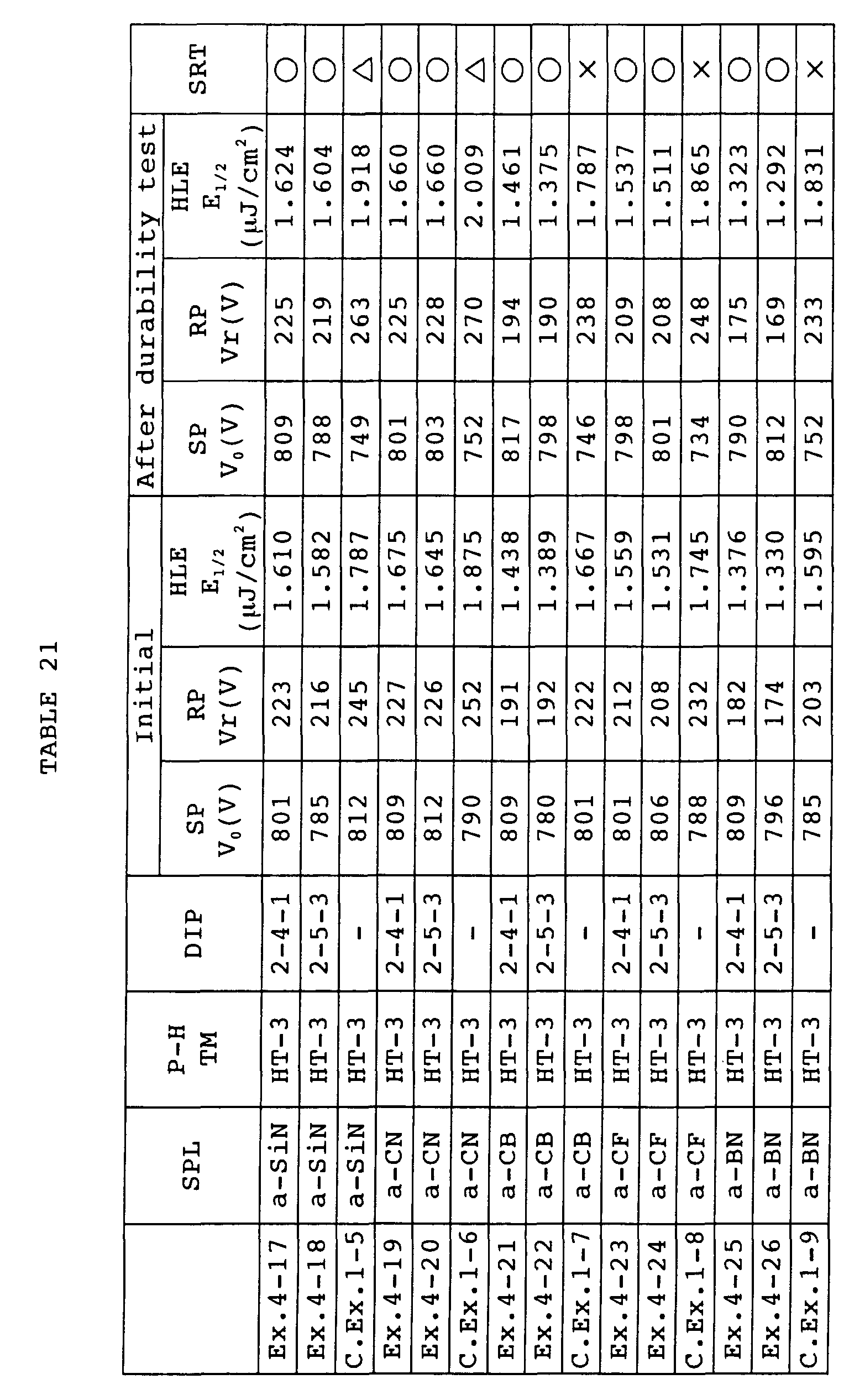
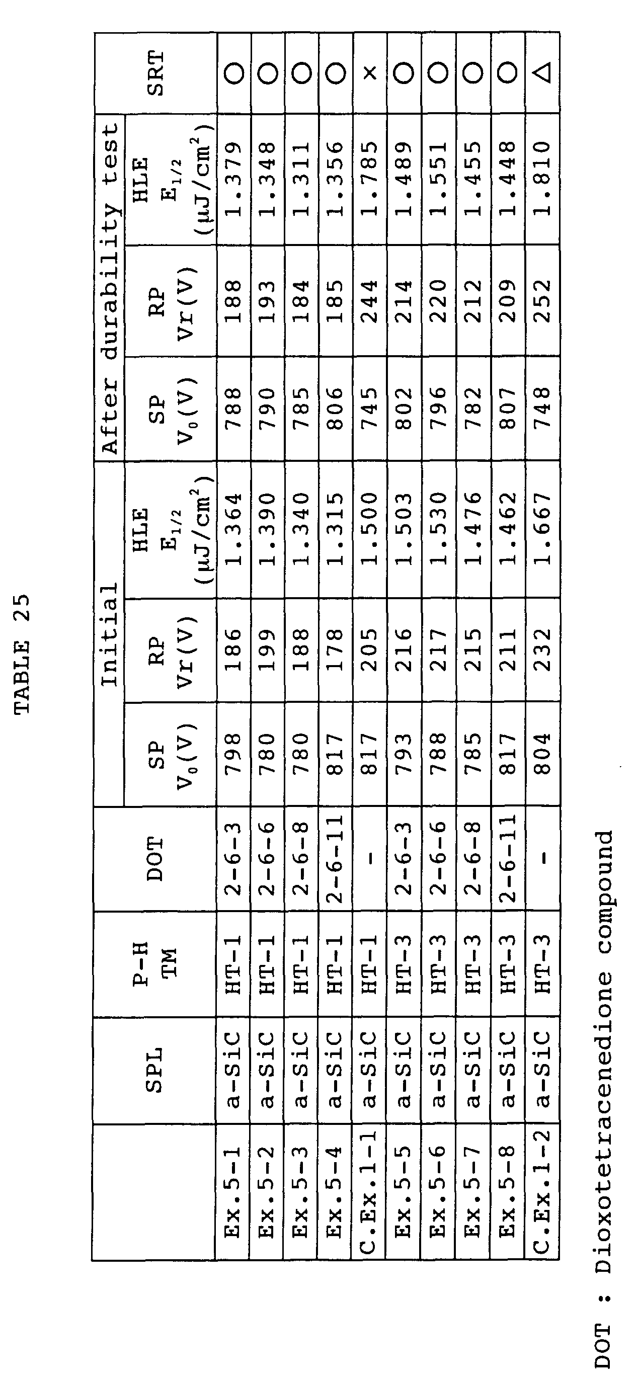
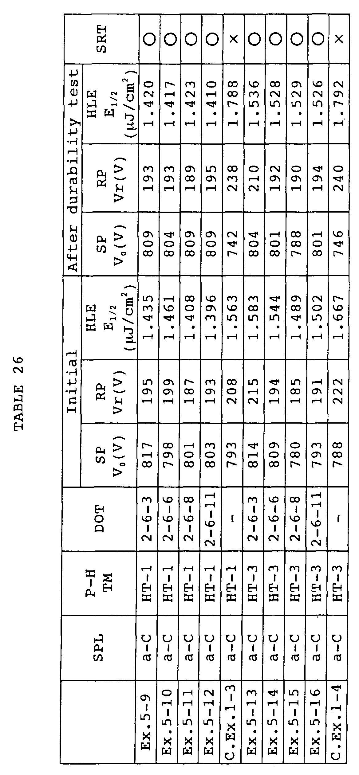
  • the electrophotosensitive materials of the above examples and comparative examples were subjected to the same photosensitivity test (I), durability test (I) and solvent resistance test as the above and evaluated for the characteristics thereof. The results are listed in Table 3.
  • electrophotosensitive materials of these comparative examples were significantly decreased in photosensitivity when formed with the surface protective layer, because they presented, in the initial stage, large residual potentials after light exposure and large half-life exposures.
  • the electrophotosensitive materials of these comparative examples were found to have poor durability because they were significantly increased in residual potential and half-life exposure after the durability test.
  • the ball mill was operated for dispersing by mixing 2.5 parts by weight of crystalline X-type metal-free phthalocyanine as the charge generating material represented by the formula (CG-1), and 1 part by weight of polyvinylbutyral as the binder resin in 15 parts by weight of tetrahydrofuran, thereby to prepare a coating solution for charge generating layer of the multi-layer photosensitive layer.
  • CG-1 crystalline X-type metal-free phthalocyanine
  • polyvinylbutyral as the binder resin in 15 parts by weight of tetrahydrofuran
  • the resultant coating solution was dip coated on the aluminum tube as the conductive substrate and then was air dried at 110°C for 30 minutes. Thus was formed a charge generating layer having a thickness of 0.5 ⁇ m.
  • the resultant coating solution was dip coated on the above charge generating layer and then was air dried at 110°C for 30 minutes, thereby to form a charge transport layer having a thickness of 20 ⁇ m.
  • a negative-charge multi-layer photosensitive layer was formed.
  • Example 1-1 The plasma CVD process was performed under the same conditions as in Example 1-1, thereby forming a surface protective layer of amorphous silicon-carbon (SiC) composite film having a thickness of 0.5 ⁇ m.
  • SiC amorphous silicon-carbon
  • Electrophotosensitive materials of Examples 1-36 to 1-40 were fabricated the same way as in Example 1-35 except that each of the examples used 0.2 parts by weight of diphenoquinone compound of the formula of a number listed in Table 4.
  • An electrophotosensitive material of Comparative Example 1-10 was fabricated the same way as in Example 1-35 except that the diphenoquinone compound was dispensed with.
  • HT-3 diethylaminobenzaldehyde diphenylhydrazone
  • Each of the electrophotosensitive materials of the above examples and comparative examples was charged at -800 ⁇ 20V and the surface potential V 0 (V) thereof was measured using a drum sensitivity tester available from GENTEC Co.
  • a bandpass filter was used to extract monochromatic light from white light from a halogen lamp as a light source of the tester, the monochromatic light having a wavelength of 780 nm and a half width of 20 nm.
  • the surface of the above electrophotosensitive material was irradiated with the monochromatic light at a light intensity of 10 ⁇ W/cm 2 for 1.0 second while the half-life exposure E 1/2 ( ⁇ J/cm 2 ) was determined by measuring the time elapsed before the surface potential V 0 (V) decreased to half.
  • the residual potential V r (V) was determined by measuring a surface potential after a lapse of 0.5 seconds from the start of the light exposure.
  • the electrophotosensitive materials of the above examples and comparative examples were each mounted in the drum sensitivity tester available from GENTEC Co.
  • the surface of each electrophotosensitive material was charged and exposed to light under the same conditions as in the photosensitivity test (II) and then was exposed to light (wavelength of 660 nm) from an erase lamp of the tester for static elimination.
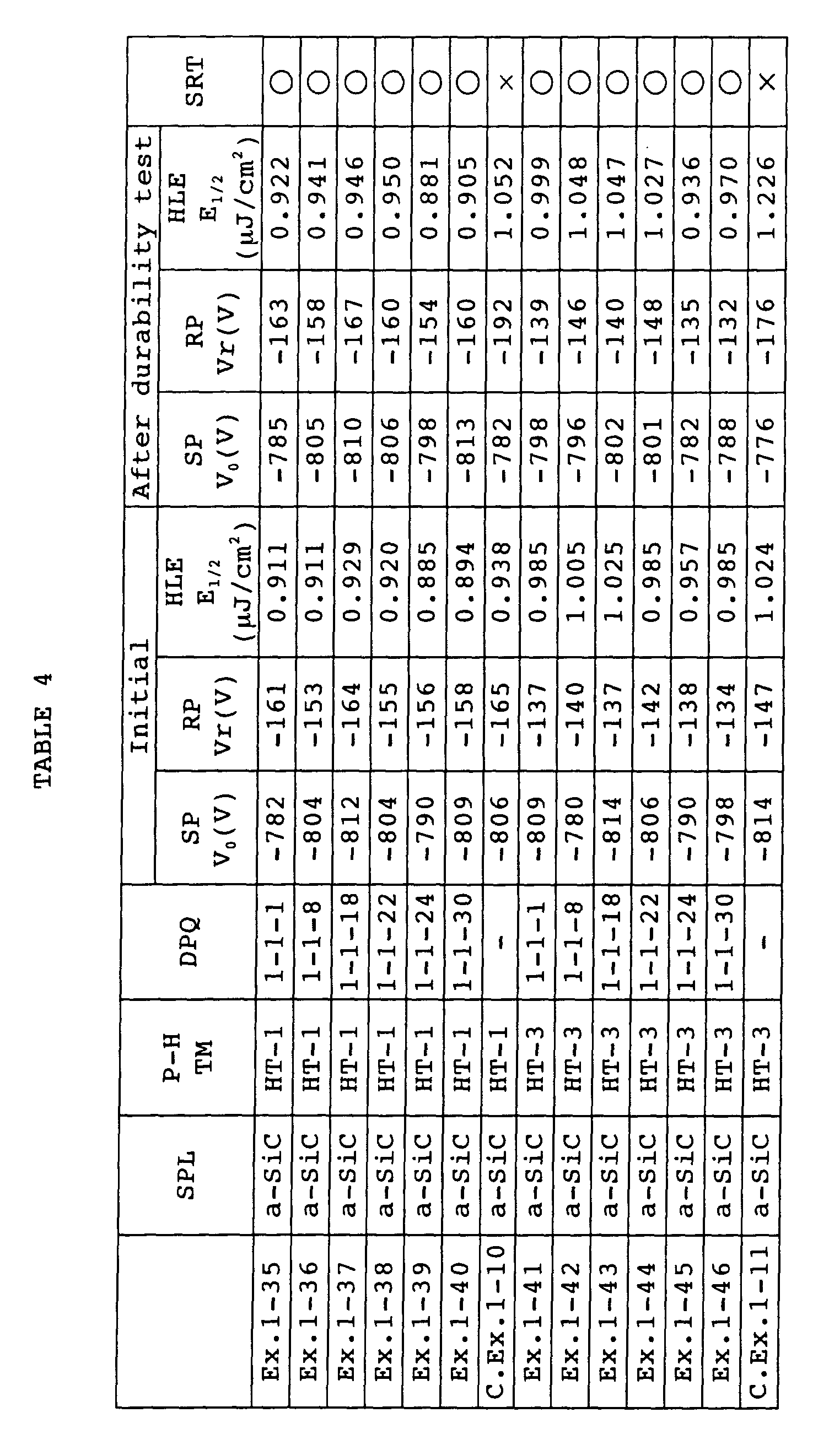
  • the process of charging, light exposure and static elimination was consecutively repeated in 2,000 cycles with a rotational speed of the electrophotosensitive material set to 40 rpm. Subsequent to the process repeated in cycles, the electrophotosensitive material was subjected to the photosensitivity test (II) again for determining the surface potential V 0 (V), half-life exposure E 1/2 ( ⁇ J/cm 2 ) and residual potential V r (V).
  • electrophotosensitive materials of these comparative examples were significantly decreased in photosensitivity when formed with the surface protective layer, because they presented, in the initial stage, large residual potentials after light exposure and large half-life exposures.
  • the electrophotosensitive materials of these comparative examples were found to have poor durability because they were significantly increased in residual potential and half-life exposure after the durability test.
  • Electrophotosensitive materials of these examples and comparative examples were fabricated the same way as in Examples 1-35 to 1-46 and Comparative Examples 1-10, 1-11, except that the same procedure as in Examples 1-13 to 1-24 and Comparative Examples 1-3, 1-4 was taken to form a surface protective layer of amorphous carbon (C) having a thickness of 0.5 ⁇ m, instead of the silicon-carbon composite film, over a surface of the multi-layer photosensitive layer.
  • C amorphous carbon
  • electrophotosensitive materials of these comparative examples were significantly decreased in photosensitivity when formed with the surface protective layer, because they presented, in the initial stage, large residual potentials after light exposure and large half-life exposures.
  • the electrophotosensitive materials of these comparative examples were found to have poor durability because they were significantly increased in residual potential and half-life exposure after the durability test.
  • Electrophotosensitive materials of these examples and comparative example were fabricated the same way as in Examples 1-45, 1-46 and Comparative Example 1-11, except that the same procedure as in Examples 1-25, 1-26 and Comparative Example 1-5 was taken to form a surface protective layer of amorphous silicon-nitrogen (SiN) composite film having a thickness of 0.5 ⁇ m, instead of the silicon-carbon composite film, over the surface of the multi-layer photosensitive layer.
  • SiN amorphous silicon-nitrogen
  • Electrophotosensitive materials of these examples and comparative example were fabricated the same way as in Examples 1-45, 1-46 and Comparative Example 1-11, except that the same procedure as in Examples 1-27, 1-28 and Comparative Example 1-6 was taken to form a surface protective layer of amorphous carbon-nitrogen (CN) composite film having a thickness of 0.5 ⁇ m, instead of the silicon-carbon composite film, over the surface of the multi-layer photosensitive layer.
  • CN amorphous carbon-nitrogen
  • Electrophotosensitive materials of these examples and comparative example were fabricated the same way as in Examples 1-45, 1-46 and Comparative Example 1-11, except that the same procedure as in Examples 1-29, 1-30 and Comparative Example 1-7 was taken to form a surface protective layer of amorphous carbon-boron (CB) composite film having a thickness of 0.5 ⁇ m, instead of the silicon-carbon composite film, over the surface of the multi-layer photosensitive layer.
  • CB amorphous carbon-boron
  • Electrophotosensitive materials of these examples and comparative example were fabricated the same way as in Examples 1-45, 1-46 and Comparative Example 1-11, except that the same procedure as in Examples 1-31, 1-32 and Comparative Example 1-8 was taken to form a surface protective layer of amorphous carbon-fluorine (CF) composite film having a thickness of 0.5 ⁇ m, instead of the silicon-carbon composite film, over the surface of the multi-layer photosensitive layer.
  • CF amorphous carbon-fluorine
  • Electrophotosensitive materials of these examples and comparative example were fabricated the same way as in Examples 1-45, 1-46 and Comparative Example 1-11, except that the same procedure as in Examples 1-33, 1-34 and Comparative Example 1-9 was taken to form a surface protective layer of amorphous boron-nitrogen (BN) composite film having a thickness of 0.5 ⁇ m, instead of the silicon-carbon composite film, over the surface of the multi-layer photosensitive layer.
  • BN amorphous boron-nitrogen
  • the electrophotosensitive materials of the above examples and comparative examples were subjected to the same photosensitivity test (II), durability test (II) and solvent resistance test as the above and were evaluated for the characteristics thereof. The results are listed in Table 6.
  • electrophotosensitive materials of these comparative examples were significantly decreased in photosensitivity when formed with the surface protective layer, because they presented, in the initial stage, large residual potentials after light exposure and large half-life exposures.
  • the electrophotosensitive materials of these comparative examples were found to have poor durability because they were significantly increased in residual potential and half-life exposure after the durability test.
  • Electrophotosensitive materials of Examples 2-1 to 2-5 were fabricated the same way as in Example 1-1, except that each of the examples used 40 parts by weight of dinaphthoquinone compound of the formula of a number listed in Table 7.
  • Electrophotosensitive materials of Examples 2-6 to 2-10 were fabricated the same way as in Example 1-7, except that each of the examples used 40 parts by weight of dinaphthoquinone compound of the formula of a number listed in Table 7.
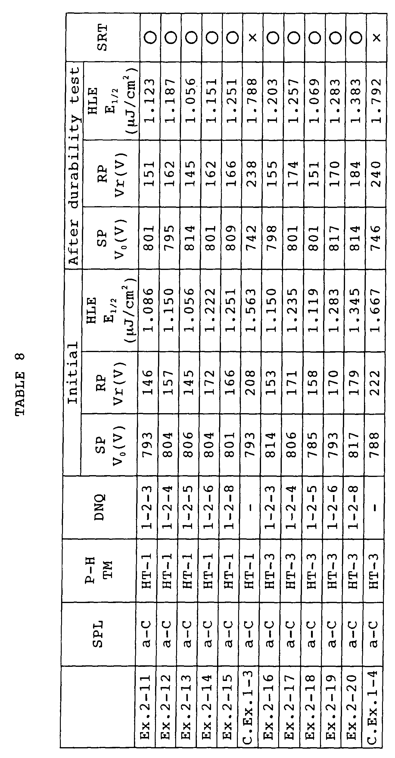
  • Electrophotosensitive materials of Examples 2-11 to 2-20 were fabricated the same way as in Examples 2-1 to 2-10, except that the same procedure as in Examples 1-13 to 1-24 was taken to form a surface protective layer of amorphous carbon (C) having a thickness of 0.5 ⁇ m, instead of the silicon-carbon composite film, over the surface of the single-layer photosensitive layer.
  • C amorphous carbon
  • Electrophotosensitive materials of Examples 2-21, 2-22 were fabricated the same way as in Examples 2-7, 2-8 except that the same procedure as in Examples 1-25, 1-26 was taken to form a surface protective layer of amorphous silicon-nitrogen (SiN) composite film having a thickness of 0.5 ⁇ m, instead of the silicon-carbon composite film, over the surface of the single-layer photosensitive layer.
  • SiN amorphous silicon-nitrogen
  • Electrophotosensitive materials of Examples 2-23, 2-24 were fabricated the same way as in Examples 2-7, 2-8 except that the same procedure as in Examples 1-27, 1-28 was taken to form a surface protective layer of amorphous carbon-nitrogen (CN) composite film having a thickness of 0.5 ⁇ m, instead of the silicon-carbon composite film, over the surface of the single-layer photosensitive layer.
  • CN amorphous carbon-nitrogen
  • Electrophotosensitive materials of Examples 2-25, 2-26 were fabricated the same way as in Examples 2-7, 2-8 except that the same procedure as in Examples 1-29, 1-30 was taken to form a surface protective layer of amorphous carbon-boron (CB) composite film having a thickness of 0.5 ⁇ m, instead of the silicon-carbon composite film, over the surface of the single-layer photosensitive layer.
  • CB amorphous carbon-boron
  • Electrophotosensitive materials of Examples 2-27, 2-28 were fabricated the same way as in Examples 2-7, 2-8 except that the same procedure as in Examples 1-31, 1-32 was taken to form a surface protective layer of amorphous carbon-fluorine (CF) composite film having a thickness of 0.5 ⁇ m, instead of the silicon-carbon composite film, over the surface of the single-layer photosensitive layer.
  • CF amorphous carbon-fluorine
  • Electrophotosensitive materials of Examples 2-29, 2-30 were fabricated the same way as in Examples 2-7, 2-8 except that the same procedure as in Examples 1-33, 1-34 was taken to form a surface protective layer of amorphous boron-nitrogen (BN) composite film having a thickness of 0.5 ⁇ m, instead of the silicon-carbon composite film, over the surface of the single-layer photosensitive layer.
  • BN amorphous boron-nitrogen
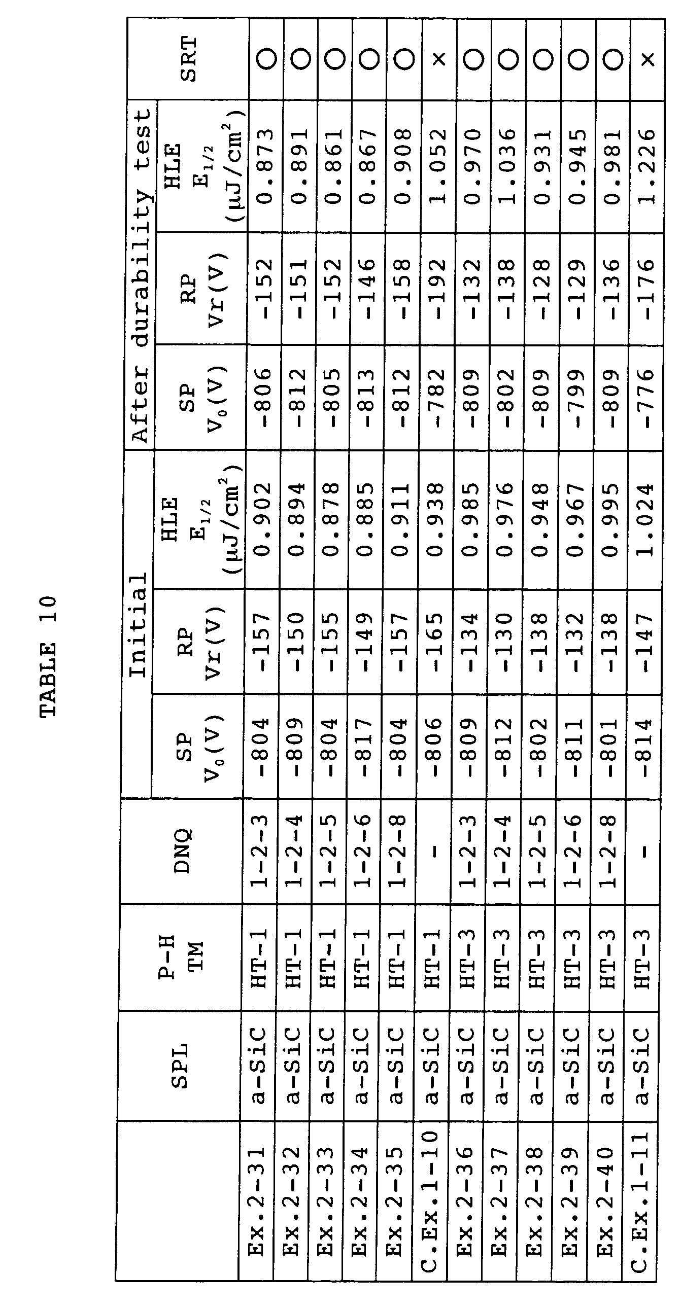
  • Electrophotosensitive materials of Examples 2-31 to 2-35 were fabricated the same way as in Example 1-35, except that each of the examples used 0.2 parts by weight of dinaphthoquinone compound of the formula of a number listed in Table 10.
  • Electrophotosensitive materials of Examples 2-36 to 2-40 were fabricated the same way as in Example 1-41, except that each of the examples used 40 parts by weight of dinaphthoquinone compound of the formula of a number listed in Table 10.
  • Electrophotosensitive materials of these examples were fabricated the same way as in Examples 2-31 to 2-40, except that the same procedure as in Examples 1-13 to 1-24 was taken to form a surface protective layer of amorphous carbon (C) having a thickness of 0.5 ⁇ m, instead of the silicon-carbon composite film, over a surface of the multi-layer photosensitive layer.
  • C amorphous carbon
  • Electrophotosensitive materials of these examples were fabricated the same way as in Examples 2-37, 2-38 except that the same procedure as in Examples 1-25, 1-26 was taken to form a surface protective layer of amorphous silicon-nitrogen (SiN) composite film having a thickness of 0.5 ⁇ m, instead of the silicon-carbon composite film, over the surface of the multi-layer photosensitive layer.
  • SiN amorphous silicon-nitrogen
  • Electrophotosensitive materials of these examples were fabricated the same way as in Examples 2-37, 2-38 except that the same procedure as in Examples 1-27, 1-28 was taken to form a surface protective layer of amorphous carbon-nitrogen (CN) composite film having a thickness of 0.5 ⁇ m, instead of the silicon-carbon composite film, over the surface of the multi-layer photosensitive layer.
  • CN amorphous carbon-nitrogen
  • Electrophotosensitive materials of these examples were fabricated the same way as in Examples 2-37, 2-38 except that the same procedure as in Examples 1-29, 1-30 was taken to form a surface protective layer of amorphous carbon-boron (CB) composite film having a thickness of 0.5 ⁇ m, instead of the silicon-carbon composite film, over the surface of the multi-layer photosensitive layer.
  • CB amorphous carbon-boron
  • Electrophotosensitive materials of these examples were fabricated the same way as in Examples 2-37, 2-38 except that the same procedure as in Examples 1-31, 1-32 was taken to form a surface protective layer of amorphous carbon-fluorine (CF) composite film having a thickness of 0.5 ⁇ m, instead of the silicon-carbon composite film, over the surface of the multi-layer photosensitive layer.
  • CF amorphous carbon-fluorine
  • Electrophotosensitive materials of these examples were fabricated the same way as in Examples 2-37, 2-38 except that the same procedure as in Examples 1-33, 1-34 was taken to form a surface protective layer of amorphous boron-nitrogen (BN) composite film having a thickness of 0.5 ⁇ m, instead of the silicon-carbon composite film, over the surface of the multi-layer photosensitive layer.
  • BN amorphous boron-nitrogen
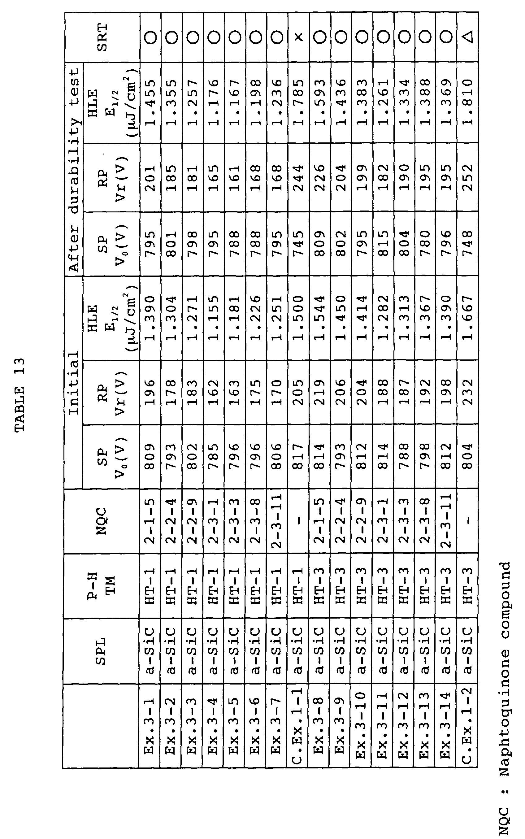
  • Electrophotosensitive materials of Examples 3-1 to 3-7 were fabricated the same way as in Example 1-1, except that each of the examples used 40 parts by weight of naphthoquinone compound of the formula of a number listed in Table 13.
  • Electrophotosensitive materials of Examples 3-8 to 3-14 were fabricated the same way as in Example 1-7, except that each of the examples used 40 parts by weight of naphthoquinone compound of the formula of a number listed in Table 13.
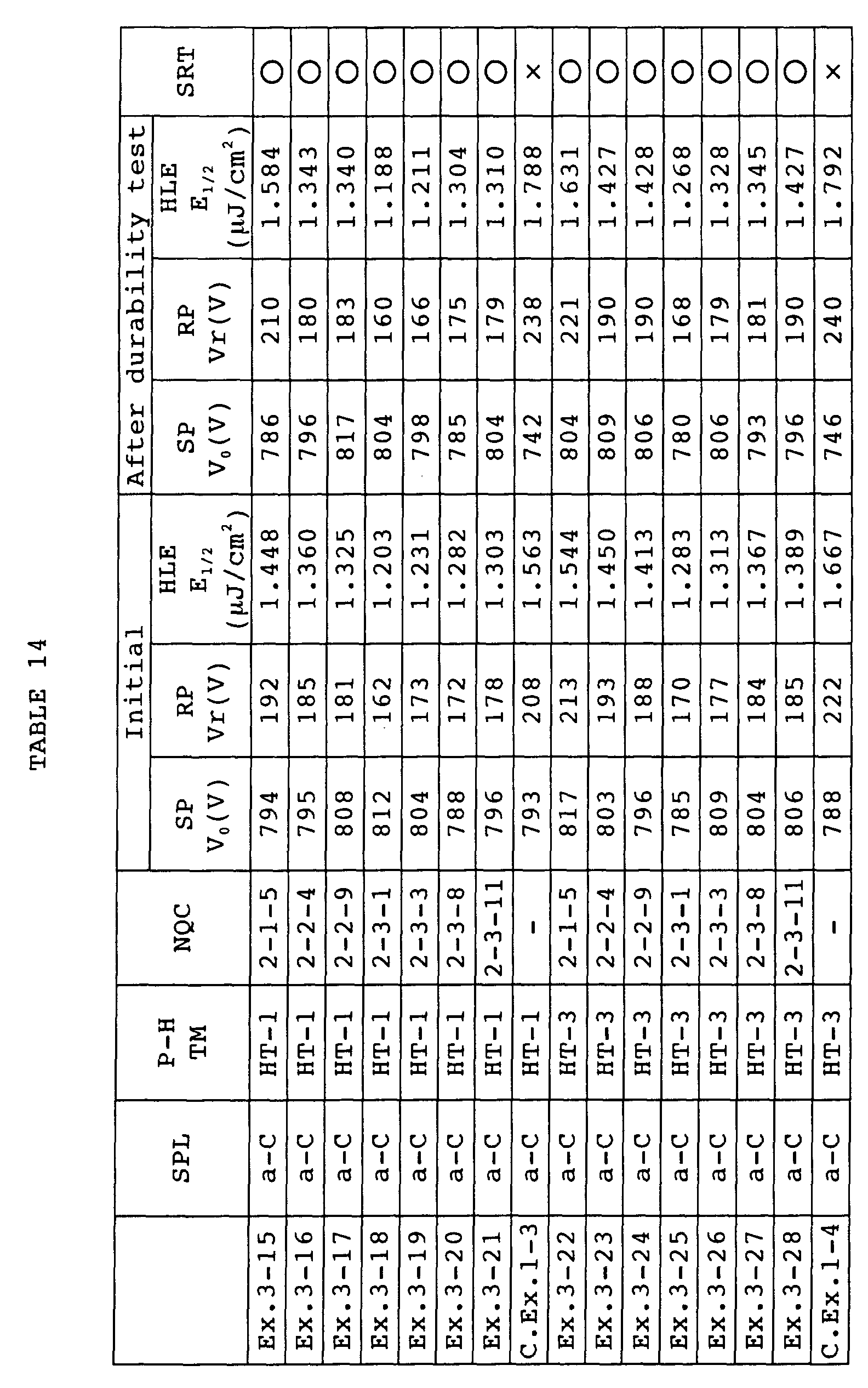
  • Electrophotosensitive materials of Examples 3-15 to 3-28 were fabricated the same way as in Examples 3-1 to 3-14 except that the same procedure as in Examples 1-13 to 1-24 was taken to form a surface protective layer of amorphous carbon (C) having a thickness of 0.5 ⁇ m, instead of the silicon-carbon composite film, over the surface of the single-layer photosensitive layer.
  • C amorphous carbon
  • Electrophotosensitive materials of Examples 3-29 to 3-32 were fabricated the same way as in Examples 3-8, 3-10, 3-12 and 3-13 except that the same procedure as in Examples 1-25, 1-26 was taken to form a surface protective layer of amorphous silicon-nitrogen (SiN) composite film having a thickness of 0.5 ⁇ m, instead of the silicon-carbon composite film, over the surface of the single-layer photosensitive layer.
  • SiN amorphous silicon-nitrogen
  • Electrophotosensitive materials of Examples 3-33 to 3-36 were fabricated the same way as in Examples 3-8, 3-10, 3-12 and 3-13 except that the same procedure as in Examples 1-27, 1-28 was taken to form a surface protective layer of amorphous carbon-nitrogen (CN) composite film having a thickness of 0.5 ⁇ m, instead of the silicon-carbon composite film, over the surface of the single-layer photosensitive layer.
  • CN amorphous carbon-nitrogen
  • Electrophotosensitive materials of Examples 3-37 to 3-40 were fabricated the same way as in Examples 3-8, 3-10, 3-12 and 3-13 except that the same procedure as in Examples 1-29, 1-30 was taken to form a surface protective layer of amorphous carbon-boron (CB) composite film having a thickness of 0.5 ⁇ m, instead of the silicon-carbon composite film, over the surface of the single-layer photosensitive layer.
  • CB amorphous carbon-boron
  • Electrophotosensitive materials of Examples 3-41 to 3-44 were fabricated the same way as in Examples 3-8, 3-10, 3-12 and 3-13 except that the same procedure as in Examples 1-31, 1-32 was taken to form a surface protective layer of amorphous carbon-fluorine (CF) composite film having a thickness of 0.5 ⁇ m, instead of the silicon-carbon composite film, over the surface of the single-layer photosensitive layer.
  • CF amorphous carbon-fluorine
  • Electrophotosensitive materials of Examples 3-45 to 3-48 were fabricated the same way as in Examples 3-8, 3-10, 3-12 and 3-13 except that the same procedure as in Examples 1-33, 1-34 was taken to form a surface protective layer of amorphous boron-nitrogen (BN) composite film having a thickness of 0.5 ⁇ m, instead of the silicon-carbon composite film, over the surface of the single-layer photosensitive layer.
  • BN amorphous boron-nitrogen
  • Electrophotosensitive materials of Examples 3-49 to 3-55 were fabricated the same way as in Example 1-35, except that each of the examples used 0.2 parts by weight of naphthoquinone compound of the formula of a number listed in Table 16.
  • Electrophotosensitive materials of Examples 3-56 to 3-62 were fabricated the same way as in Example 1-41, except that each of the examples used 40 parts by weight of naphthoquinone compound of the formula of a number listed in Table 16.
  • Electrophotosensitive materials of these examples were fabricated the same way as in Examples 3-49 to 3-62 except that the same procedure as in Examples 1-13 to 1-24 was taken to form a surface protective layer of amorphous carbon (C) having a thickness of 0.5 ⁇ m, instead of the silicon-carbon composite film, over the surface of the multi-layer photosensitive layer.
  • C amorphous carbon
  • Electrophotosensitive materials of these examples were fabricated the same way as in Examples 3-56, 3-58, 3-60 and 3-61 except that the same procedure as in Examples 1-25, 1-26 was taken to form a surface protective layer of amorphous silicon-nitrogen (SiN) composite film having a thickness of 0.5 ⁇ m, instead of the silicon-carbon composite film, over the surface of the multi-layer photosensitive layer.
  • SiN amorphous silicon-nitrogen
  • Electrophotosensitive materials of these examples were fabricated the same way as in Examples 3-56, 3-58, 3-60 and 3-61 except that the same procedure as in Examples 1-27, 1-28 was taken to form a surface protective layer of amorphous carbon-nitrogen (CN) composite film having a thickness of 0.5 ⁇ m, instead of the silicon-carbon composite film, over the surface of the multi-Layer photosensitive layer.
  • CN amorphous carbon-nitrogen
  • Electrophotosensitive materials of these examples were fabricated the same way as in Examples 3-56, 3-58, 3-60 and 3-61 except that the same procedure as in Examples 1-29, 1-30 was taken to form a surface protective layer of amorphous carbon-boron (CB) composite film having a thickness of 0.5 ⁇ m, instead of the silicon-carbon composite film, over the surface of the multi-layer photosensitive layer.
  • CB amorphous carbon-boron
  • Electrophotosensitive materials of these examples were fabricated the same way as in Examples 3-56, 3-58, 3-60 and 3-61 except that the same procedure as in Examples 1-31, 1-32 was taken to form a surface protective layer of amorphous carbon-fluorine (CF) composite film having a thickness of 0.5 ⁇ m, instead of the silicon-carbon composite film, over the surface of the multi-layer photosensitive layer.
  • CF amorphous carbon-fluorine
  • Electrophotosensitive materials of these examples were fabricated the same way as in Examples 3-56, 3-58, 3-60 and 3-61 except that the same procedure as in Examples 1-33, 1-34 was taken to form a surface protective layer of amorphous boron-nitrogen (BN) composite film having a thickness of 0.5 ⁇ m, instead of the silicon-carbon composite film, over the surface of the multi-layer photosensitive layer.
  • BN amorphous boron-nitrogen
  • Electrophotosensitive materials of Examples 4-1 to 4-4 were fabricated the same way as in Example 1-1 except that each of the examples used 40 parts by weight of diindenopyrazine compound of the formula of a number listed in Table 19.
  • Electrophotosensitive materials of Examples 4-5 to 4-8 were fabricated the same way as in Example 1-7 except that each of the examples used 40 parts by weight of diindenopyrazine compound of the formula of a number listed in Table 19.
  • Electrophotosensitive materials of Examples 4-9 to 4-16 were fabricated the same way as in Examples 4-1 to 4-8 except that the same procedure as in Examples 1-13 to 1-24 was taken to form a surface protective layer of amorphous carbon (C) having a thickness of 0.5 ⁇ m, instead of the silicon-carbon composite film, over the surface of the single-layer photosensitive layer.
  • C amorphous carbon
  • the electrophotosensitive materials of the above examples were subjected to the same photosensitivity test (I), durability test (I) and solvent resistance test as the above and were evaluated for the characteristics thereof.
  • the results as well as those of Comparative Examples 1-3, 1-4 are listed in Table 20.
  • Electrophotosensitive materials of Examples 4-17, 4-18 were fabricated the same way as in Examples 4-5, 4-8 except that the same procedure as in Examples 1-25, 1-26 was taken to form a surface protective layer of amorphous silicon-nitrogen (SiN) composite film having a thickness of 0.5 ⁇ m, instead of the silicon-carbon composite film, over the surface of the single-layer photosensitive layer.
  • SiN amorphous silicon-nitrogen
  • Electrophotosensitive materials of Examples 4-19, 4-20 were fabricated the same way as in Examples 4-5, 4-8 except that the same procedure as in Examples 1-27, 1-28 was taken to form a surface protective layer of amorphous carbon-nitrogen (CN) composite film having a thickness of 0.5 ⁇ m, instead of the silicon-carbon composite film, over the surface of the single-layer photosensitive layer.
  • CN amorphous carbon-nitrogen
  • Electrophotosensitive materials of Examples 4-21, 4-22 were fabricated the same way as in Examples 4-5, 4-8 except that the same procedure as in Examples 1-29, 1-30 was taken to form a surface protective layer of amorphous carbon-boron (CB) composite film having a thickness of 0.5 ⁇ m, instead of the silicon-carbon composite film, over the surface of the single-layer photosensitive layer.
  • CB amorphous carbon-boron
  • Electrophotosensitive materials of Examples 4-23, 4-24 were fabricated the same way as in Examples 4-5, 4-8 except that the same procedure as in Examples 1-31, 1-32 was taken to form a surface protective layer of amorphous carbon-fluorine (CF) composite film having a thickness of 0.5 ⁇ m, instead of the silicon-carbon composite film, over the surface of the single-layer photosensitive layer.
  • CF amorphous carbon-fluorine
  • Electrophotosensitive materials of Examples 4-25, 4-26 were fabricated the same way as in Examples 4-5, 4-8 except that the same procedure as in Examples 1-33, 1-34 was taken to form a surface protective layer of amorphous boron-nitrogen (BN) composite film having a thickness of 0.5 ⁇ m, instead of the silicon-carbon composite film, over the surface of the single-layer photosensitive layer.
  • BN amorphous boron-nitrogen
  • the electrophotosensitive materials of the above examples were subjected to the same photosensitivity test (I), durability test (I) and solvent resistance test as the above and were evaluated for the characteristics thereof.
  • the results as well as those of Comparative Examples 1-5 to 1-9 are listed in Table 21.
  • Electrophotosensitive materials of Examples 4-27 to 4-30 were fabricated the same way as in Example 1-35 except that each of the examples used 0.2 parts by weight of diindenopyrazine compound of the formula of a number listed in Table 22.
  • Electrophotosensitive materials of Examples 4-31 to 4-34 were fabricated the same way as in Example 1-41 except that each of the examples used 40 parts by weight of diindenopyrazine compound of the formula of a number listed in Table 22.
  • the electrophotosensitive materials of the above examples were subjected to the same photosensitivity test (II), durability test (II) and solvent resistance test as the above and were evaluated for the characteristics thereof.
  • the results as well as those of Comparative Examples 1-10, 1-11 are listed in Table 22.
  • Electrophotosensitive materials of these examples were fabricated the same way as in Examples 4-27 to 4-34 except that the same procedure as in Examples 1-13 to 1-24 was taken to form a surface protective layer of amorphous carbon (C) having a thickness of 0.5 ⁇ m, instead of the silicon-carbon composite film, over the surface of the multi-layer photosensitive layer.
  • C amorphous carbon
  • the electrophotosensitive materials of the above examples were subjected to the same photosensitivity test (II), durability test (II) and solvent resistance test as the above and were evaluated for the characteristics thereof.
  • the results as well as those of Comparative Examples 1-12, 1-13 are listed in Table 23.
  • Electrophotosensitive materials of these examples were fabricated the same way as in Examples 4-31, 4-34 except that the same procedure as in Examples 1-25, 1-26 was taken to form a surface protective layer of amorphous silicon-nitrogen (SiN) composite film having a thickness of 0.5 ⁇ m, instead of the silicon-carbon composite film, over the surface of the multi-layer photosensitive layer.
  • SiN amorphous silicon-nitrogen
  • Electrophotosensitive materials of these examples were fabricated the same way as in Examples 4-31, 4-34 except that the same procedure as in Examples 1-27, 1-28 was taken to form a surface protective layer of amorphous carbon-nitrogen (CN) composite film having a thickness of 0.5 ⁇ m, instead of the silicon-carbon composite film, over the surface of the multi-layer photosensitive layer.
  • CN amorphous carbon-nitrogen
  • Electrophotosensitive materials of these examples were fabricated the same way as in Examples 4-31, 4-34 except that the same procedure as in Examples 1-29, 1-30 was taken to form a surface protective layer of amorphous carbon-boron (CB) composite film having a thickness of 0.5 ⁇ m, instead of the silicon-carbon composite film, over the surface of the multi-layer photosensitive layer.
  • CB amorphous carbon-boron
  • Electrophotosensitive materials of these examples were fabricated the same way as in Examples 4-31, 4-34 except that the same procedure as in Examples 1-31, 1-32 was taken to form a surface protective layer of amorphous carbon-fluorine (CF) composite film having a thickness of 0.5 ⁇ m, instead of the silicon-carbon composite film, over the surface of the multi-layer photosensitive layer.
  • CF amorphous carbon-fluorine
  • Electrophotosensitive materials of these examples were fabricated the same way as in Examples 4-31, 4-34 except that the same procedure as in Examples 1-33, 1-34 was taken to form a surface protective layer of amorphous boron-nitrogen (BN) composite film having a thickness of 0.5 ⁇ m, instead of the silicon-carbon composite film, over the surface of the multi-layer photosensitive layer.
  • BN amorphous boron-nitrogen
  • the electrophotosensitive materials of the above examples were subjected to the same photosensitivity test (II), durability test (II) and solvent resistance test as the above and were evaluated for the characteristics thereof.
  • the results as well as those of Comparative Examples 1-14 to 1-18 are listed in Table 24.
  • Electrophotosensitive materials of Examples 5-1 to 5-4 were fabricated the same way as in Example 1-1 except that each of the examples used 40 parts by weight of dioxotetracenedione compound of the formula of a number listed in Table 25.
  • Electrophotosensitive materials of Examples 5-5 to 5-8 were fabricated the same way as in Example 1-7 except that each of the examples used 40 parts by weight of dioxotetracenedione compound of the formula of a number listed in Table 25.
  • Electrophotosensitive materials of Examples 5-9 to 5-16 were fabricated the same way as in Examples 5-1 to 5-8 except that the same procedure as in Examples 1-13 to 1-24 was taken to form a surface protective layer of amorphous carbon (C) having a thickness of 0.5 ⁇ m, instead of the silicon-carbon composite film, over the surface of the single-layer photosensitive layer.
  • C amorphous carbon
  • the electrophotosensitive materials of the above examples were subjected to the same photosensitivity test (I), durability test (I) and solvent resistance test as the above and were evaluated for the characteristics thereof.
  • the results as well as those of Comparative Examples 1-3, 1-4 are listed in Table 26.
  • Electrophotosensitive materials of Examples 5-17, 5-18 were fabricated the same way as in Examples 5-5, 5-7 except that the same procedure as in Examples 1-25, 1-26 was taken to form a surface protective layer of amorphous silicon-nitrogen (SiN) composite film having a thickness of 0.5 ⁇ m, instead of the silicon-carbon composite film, over the surface of the single-layer photosensitive layer.
  • SiN amorphous silicon-nitrogen
  • Electrophotosensitive materials of Examples 5-19, 5-20 were fabricated the same way as in Examples 5-5, 5-7 except that the same procedure as in Examples 1-27, 1-28 was taken to form a surface protective layer of amorphous carbon-nitrogen (CN) composite film having a thickness of 0.5 ⁇ m, instead of the silicon-carbon composite film, over the surface of the single-layer photosensitive layer.
  • CN amorphous carbon-nitrogen
  • Electrophotosensitive materials of Examples 5-21, 5-22 were fabricated the same way as in Examples 5-5, 5-7 except that the same procedure as in Examples 1-29, 1-30 was taken to form a surface protective layer of amorphous carbon-boron (CB) composite film having a thickness of 0.5 ⁇ m, instead of the silicon-carbon composite film, over the surface of the single-layer photosensitive layer.
  • CB amorphous carbon-boron
  • Electrophotosensitive materials of Examples 5-23, 5-24 were fabricated the same way as in Examples 5-5, 5-7 except that the same procedure as in Examples 1-31, 1-32 was taken to form a surface protective layer of amorphous carbon-fluorine (CF) composite film having a thickness of 0.5 ⁇ m, instead of the silicon-carbon composite film, over the surface of the single-layer photosensitive layer.
  • CF amorphous carbon-fluorine
  • Electrophotosensitive materials of Examples 5-25, 5-26 were fabricated the same way as in Examples 5-5, 5-7 except that the same procedure as in Examples 1-33, 1-34 was taken to form a surface protective layer of amorphous boron-nitrogen (BN) composite film having a thickness of 0.5 ⁇ m, instead of the silicon-carbon composite film, over the surface of the single-layer photosensitive layer.
  • BN amorphous boron-nitrogen
  • the electrophotosensitive materials of the above examples were subjected to the same photosensitivity test (I), durability test (I) and solvent resistance test as the above and were evaluated for the characteristics thereof.
  • the results as well as those of Comparative Examples 1-5 to 1-9 are listed in Table 27.
  • Electrophotosensitive materials of Examples 5-27 to 5-30 were fabricated the same way as in Example 1-35 except that each of the examples used 0.2 parts by weight of dioxotetracenedione compound of the formula of a number listed in Table 28.
  • Electrophotosensitive materials of Examples 5-31 to 5-34 were fabricated the same way as in Example 1-41 except that each of the examples used 40 parts by weight of dioxotetracenedione compound of the formula of a number listed in Table 28.
  • the electrophotosensitive materials of the above examples were subjected to the same photosensitivity test (II), durability test (II) and solvent resistance test as the above and were evaluated for the characteristics thereof.
  • the results as well as those of Comparative Examples 1-10, 1-11 are listed in Table 28.
  • Electrophotosensitive materials of these examples were fabricated the same way as in Examples 5-27 to 5-34 except that the same procedure as in Examples 1-13 to 1-24 was taken to form a surface protective layer of amorphous carbon (C) having a thickness of 0.5 ⁇ m, instead of the silicon-carbon composite film, over the surface of the multi-layer photosensitive layer.
  • C amorphous carbon
  • the electrophotosensitive materials of the above examples were subjected to the same photosensitivity test (II), durability test (II) and solvent resistance test as the above and were evaluated for the characteristics thereof.
  • the results as well as those of Comparative Examples 1-12, 1-13 are listed in Table 29.
  • Electrophotosensitive materials of these examples were fabricated the same way as in Examples 5-31, 5-33 except that the same procedure as in Examples 1-25, 1-26 was taken to form a surface protective layer of amorphous silicon-nitrogen (SiN) composite film having a thickness of 0.5 ⁇ m, instead of the silicon-carbon composite film, over the surface of the multi-layer photosensitive layer.
  • SiN amorphous silicon-nitrogen
  • Electrophotosensitive materials of these examples were fabricated the same way as in Examples 5-31, 5-33 except that the same procedure as in Examples 1-27, 1-28 was taken to form a surface protective layer of amorphous carbon-nitrogen (CN) composite film having a thickness of 0.5 ⁇ m, instead of the silicon-carbon composite film, over the surface of the multi-layer photosensitive layer.
  • CN amorphous carbon-nitrogen
  • Electrophotosensitive materials of these examples were fabricated the same way as in Examples 5-31, 5-33 except that the same procedure as in Examples 1-29, 1-30 was taken to form a surface protective layer of amorphous carbon-boron (CB) composite film having a thickness of 0.5 ⁇ m, instead of the silicon-carbon composite film, over the surface of the multi-layer photosensitive layer.
  • CB amorphous carbon-boron
  • Electrophotosensitive materials of these examples were fabricated the same way as in Examples 5-31, 5-33 except that the same procedure as in Examples 1-31, 1-32 was taken to form a surface protective layer of amorphous carbon-fluorine (CF) composite film having a thickness of 0.5 ⁇ m, instead of the silicon-carbon composite film, over the surface of the multi-layer photosensitive layer.
  • CF amorphous carbon-fluorine
  • Electrophotosensitive materials of these examples were fabricated the same way as in Examples 5-31, 5-33 except that the same procedure as in Examples 1-33, 1-34 was taken to form a surface protective layer of amorphous boron-nitrogen (BN) composite film having a thickness of 0.5 ⁇ m, instead of the silicon-carbon composite film, over the surface of the multi-layer photosensitive layer.
  • BN amorphous boron-nitrogen
  • the electrophotosensitive materials of the above examples were subjected to the same photosensitivity test (II), durability test (II) and solvent resistance test as the above and were evaluated for the characteristics thereof.
  • the results as well as those of Comparative Examples 1-14 to 1-18 are listed in Table 30.
  • Electrophotosensitive materials of Examples 6-1 to 6-4 were fabricated the same way as in Example 1-1 except that each of the examples used 40 parts by weight of naphthylene diimide derivative of the formula of a number listed in Table 31.
  • Electrophotosensitive materials of Examples 6-5 to 6-8 were fabricated the same way as in Example 1-7 except that each of the examples used 40 parts by weight of naphthylene diimide derivative of the formula of a number listed in Table 31.
  • Electrophotosensitive materials of Examples 6-9 to 6-16 were fabricated the same way as in Examples 6-1 to 6-8 except that the same procedure as in Examples 1-13 to 1-24 was taken to form a surface protective layer of amorphous carbon (C) having a thickness of 0.5 ⁇ m, instead of the silicon-carbon composite film, over the surface of the single-layer photosensitive layer.
  • C amorphous carbon
  • the electrophotosensitive materials of the above examples were subjected to the same photosensitivity test (I), durability test (I) and solvent resistance test as the above and were evaluated for the characteristics thereof.
  • the results as well as those of Comparative Examples 1-3, 1-4 are listed in Table 32.
  • Electrophotosensitive materials of Examples 6-17, 6-18 were fabricated the same way as in Examples 6-5, 6-8 except that the same procedure as in Examples 1-25, 1-26 was taken to form a surface protective layer of amorphous silicon-nitrogen (SiN) composite film having a thickness of 0.5 ⁇ m, instead of the silicon-carbon composite film, over the surface of the single-layer photosensitive layer.
  • SiN amorphous silicon-nitrogen
  • Electrophotosensitive materials of Examples 6-19, 6-20 were fabricated the same way as in Examples 6-5, 6-8 except that the same procedure as in Examples 1-27, 1-28 was taken to form a surface protective layer of amorphous carbon-nitrogen (CN) composite film having a thickness of 0.5 ⁇ m, instead of the silicon-carbon composite film, over the surface of the single-layer photosensitive layer.
  • CN amorphous carbon-nitrogen
  • Electrophotosensitive materials of Examples 6-21, 6-22 were fabricated the same way as in Examples 6-5, 6-8 except that the same procedure as in Examples 1-29, 1-30 was taken to form a surface protective layer of amorphous carbon-boron (CB) composite film having a thickness of 0.5 ⁇ m, instead of the silicon-carbon composite film, over the surface of the single-layer photosensitive layer.
  • CB amorphous carbon-boron
  • Electrophotosensitive materials of Examples 6-23, 6-24 were fabricated the same way as in Examples 6-5, 6-8 except that the same procedure as in Examples 1-31, 1-32 was taken to form a surface protective layer of amorphous carbon-fluorine (CF) composite film having a thickness of 0.5 ⁇ m, instead of the silicon-carbon composite film, over the surface of the single-layer photosensitive layer.
  • CF amorphous carbon-fluorine
  • Electrophotosensitive materials of Examples 6-25, 6-26 were fabricated the same way as in Examples 6-5, 6-8 except that the same procedure as in Examples 1-33, 1-34 was taken to form a surface protective layer of amorphous boron-nitrogen (BN) composite film having a thickness of 0.5 ⁇ m, instead of the silicon-carbon composite film, over the surface of the single-layer photosensitive layer.
  • BN amorphous boron-nitrogen
  • the electrophotosensitive materials of the above examples were subjected to the same photosensitivity test (I), durability test (I) and solvent resistance test as the above and were evaluated for the characteristics thereof.
  • the results as well as those of Comparative Examples 1-5 to 1-9 are listed in Table 33.
  • Electrophotosensitive materials of Examples 6-27 to 6-30 were fabricated the same way as in Example 1-35 except that each of the examples used 0.2 parts by weight of naphthylene diimide derivative of the formula of a number listed in Table 34.
  • Electrophotosensitive materials of Examples 6-31 to 6-34 were fabricated the same way as in Example 1-41 except that each of the examples used 40 parts by weight of naphthylene diimide derivative of the formula of a number listed in Table 34.
  • the electrophotosensitive materials of the above examples were subjected to the same photosensitivity test (II), durability test (II) and solvent resistance test as the above and were evaluated for the characteristics thereof.
  • the results as well as those of Comparative Examples 1-10, 1-11 are listed in Table 34.
  • Electrophotosensitive materials of these examples were fabricated the same way as in Examples 6-27 to 6-34 except that the same procedure as in Examples 1-13 to 1-24 was taken to form a surface protective layer of amorphous carbon (C) having a thickness of 0.5 ⁇ m, instead of the silicon-carbon composite film, over the surface of the multi-layer photosensitive layer.
  • C amorphous carbon
  • the electrophotosensitive materials of the above examples were subjected to the same photosensitivity test (II), durability test (II) and solvent resistance test as the above and were evaluated for the characteristics thereof.
  • the results as well as those of Comparative Examples 1-12, 1-13 are listed in Table 35.
  • Electrophotosensitive materials of these examples were fabricated the same way as in Examples 6-31, 6-34 except that the same procedure as in Examples 1-25, 1-26 was taken to form a surface protective layer of amorphous silicon-nitrogen (SiN) composite film having a thickness of 0.5 ⁇ m, instead of the silicon-carbon composite film, over the surface of the multi-layer photosensitive layer
  • Electrophotosensitive materials of these examples were fabricated the same way as in Examples 6-31, 6-34 except that the same procedure as in Examples 1-27, 1-28 was taken to form a surface protective layer of amorphous carbon-nitrogen (CN) composite film having a thickness of 0.5 ⁇ m, instead of the silicon-carbon composite film, over the surface of the multi-layer photosensitive layer.
  • CN amorphous carbon-nitrogen
  • Electrophotosensitive materials of these examples were fabricated the same way as in Examples 6-31, 6-34 except that the same procedure as in Examples 1-29, 1-30 was taken to form a surface protective layer of amorphous carbon-boron (CB) composite film having a thickness of 0.5 ⁇ m, instead of the silicon-carbon composite film, over the surface of the multi-layer photosensitive layer.
  • CB amorphous carbon-boron
  • Electrophotosensitive materials of these examples were fabricated the same way as in Examples 6-31, 6-34 except that the same procedure as in Examples 1-31, 1-32 was taken to form a surface protective layer of amorphous carbon-fluorine (CF) composite film having a thickness of 0.5 ⁇ m, instead of the silicon-carbon composite film, over the surface of the multi-layer photosensitive layer.
  • CF amorphous carbon-fluorine
  • Electrophotosensitive materials of these examples were fabricated the same way as in Examples 6-31, 6-34 except that the same procedure as in Examples 1-33, 1-34 was taken to form a surface protective layer of amorphous boron-nitrogen (BN) composite film having a thickness of 0.5 ⁇ m, instead of the silicon-carbon composite film, over the surface of the multi-layer photosensitive layer.
  • BN amorphous boron-nitrogen
  • the electrophotosensitive materials of the above examples were subjected to the same photosensitivity test (II), durability test (II) and solvent resistance test as the above and were evaluated for the characteristics thereof.
  • the results as well as those of Comparative Examples 1-14 to 1-18 are listed in Table 36.
  • Electrophotosensitive materials of Examples 7-1 to 7-7 were fabricated the same way as in Example 1-1 except that each of the examples used 40 parts by weight of quinone derivative of the formula of a number listed in Table 37.
  • An electrophotosensitive material of Comparative Example 7-1 was fabricated the same way as in Examples 7-1 to 7-7 except that 40 parts by weight of isatin compound represented by the formula (ET-1) was used instead of the quinone derivative.
  • Electrophotosensitive materials of Examples 7-8 to 7-14 were fabricated the same way as in Example 1-7 except that each of the examples used 40 parts by weight of quinone derivative of the formula of a number listed in Table 37.
  • An electrophotosensitive material of Comparative Example 7-2 was fabricated the same way as in Examples 7-8 to 7-14 except that 40 parts by weight of isatin compound represented by the formula (ET-1) was used instead of the quinone derivative.
  • the electrophotosensitive materials of these comparative examples were found to have poor durability because they were significantly increased in residual potential and half-life exposure after the durability test.
  • Electrophotosensitive materials of Examples 7-15 to 7-28 and Comparative Examples 7-3, 7-4 were fabricated the same way as in Examples 7-1 to 7-14 and Comparative Examples 7-1, 7-2 except that the same procedure as in Examples 1-13 to 1-24 was taken to form a surface protective layer of amorphous carbon (C) having a thickness of 0.5 ⁇ m, instead of the silicon-carbon composite film, over the surface of the single-layer photosensitive layer.
  • C amorphous carbon
  • the electrophotosensitive materials of these comparative examples were found to have poor durability because they were significantly increased in residual potential and half-life exposure after the durability test.
  • Electrophotosensitive materials of Examples 7-29 to 7-32 and Comparative Example 7-5 were fabricated the same way as in Examples 7-8, 7-10, 7-11 and 7-13 and Comparative Example 7-2 except that the same procedure as in Examples 1-25, 1-26 was taken to form a surface protective layer of amorphous silicon-nitrogen (SiN) composite film having a thickness of 0.5 ⁇ m, instead of the silicon-carbon composite film, over the surface of the single-layer photosensitive layer.
  • SiN amorphous silicon-nitrogen
  • Electrophotosensitive materials of Examples 7-33 to 7-36 and Comparative Example 7-6 were fabricated the same way as in Examples 7-8, 7-10, 7-11 and 7-13 and Comparative Example 7-2 except that the same procedure as in Examples 1-27, 1-28 was taken to form a surface protective layer of amorphous carbon-nitrogen (CN) composite film having a thickness of 0.5 ⁇ m, instead of the silicon-carbon composite film, over the surface of the single-layer photosensitive layer.
  • CN amorphous carbon-nitrogen
  • Electrophotosensitive materials of Examples 7-37 to 7-40 and Comparative Example 7-7 were fabricated the same way as in Examples 7-8, 7-10, 7-11 and 7-13 and Comparative Example 7-2 except that the same procedure as in Examples 1-29, 1-30 was taken to form a surface protective layer of amorphous carbon-boron (CB) composite film having a thickness of 0.5 ⁇ m, instead of the silicon-carbon composite film, over the surface of the single-layer photosensitive layer.
  • CB amorphous carbon-boron
  • Electrophotosensitive materials of Examples 7-41 to 7-44 and Comparative Example 7-8 were fabricated the same way as in Examples 7-8, 7-10, 7-11 and 7-13 and Comparative Example 7-2 except that the same procedure as in Examples 1-31, 1-32 was taken to form a surface protective layer of amorphous carbon-fluorine (CF) composite film having a thickness of 0.5 ⁇ m, instead of the silicon-carbon composite film, over the surface of the single-layer photosensitive layer.
  • CF amorphous carbon-fluorine
  • Electrophotosensitive materials of Examples 7-45 to 7-48 and Comparative Example 7-9 were fabricated the same way as in Examples 7-8, 7-10, 7-11 and 7-13 and Comparative Example 7-2 except that the same procedure as in Examples 1-33, 1-34 was taken to form a surface protective layer of amorphous boron-nitrogen (BN) composite film having a thickness of 0.5 ⁇ m, instead of the silicon-carbon composite film, over the surface of the single-layer photosensitive layer.
  • BN amorphous boron-nitrogen
  • the electrophotosensitive materials of these comparative examples were found to have poor durability because they were significantly increased in residual potential and half-life exposure after the durability test.
  • Electrophotosensitive materials of Examples 7-49 to 7-55 were fabricated the same way as in Example 1-35 except that each of the examples used 0.2 parts by weight of quinone derivative of the formula of a number listed in Table 40.
  • An electrophotosensitive material of Comparative Example 7-10 was fabricated the same way as in Examples 7-49 to 7-55 except that 0.2 parts by weight of isatin compound represented by the formula (ET-1) was used instead of the quinone derivative.
  • Electrophotosensitive materials of Examples 7-56 to 7-62 were fabricated the same way as in Example 1-41 except that each of the examples used 40 parts by weight of quinone derivative of the formula of a number listed in Table 40.
  • An electrophotosensitive material of Comparative Example 7-11 was fabricated the same way as in Examples 7-56 to 7-62 except that 0.2 parts by weight of isatin compound represented by the formula (ET-1) was used instead of the quinone derivative.
  • the electrophotosensitive materials of the above examples and comparative examples were subjected to the same photosensitivity test (II), durability test (II) and solvent resistance test as the above and were evaluated for the characteristics thereof.
  • the results as well as those of Comparative Examples 1-10, 1-11 are listed in Table 40.
  • the electrophotosensitive materials of these comparative examples were found to have poor durability because they were significantly increased in residual potential and half-life exposure after the durability test.
  • Electrophotosensitive materials of these examples and comparative examples were fabricated the same way as in Examples 7-49 to 7-62 and Comparative Examples 7-10, 7-11 except that the same procedure as in Examples 1-13 to 1-24 was taken to form a surface protective layer of amorphous carbon (C) having a thickness of 0.5 ⁇ m, instead of the silicon-carbon composite film, over the surface of the multi-layer photosensitive layer.
  • C amorphous carbon
  • the electrophotosensitive materials of the above examples and comparative examples were subjected to the same photosensitivity test (II), durability test (II) and solvent resistance test as the above and were evaluated for the characteristics thereof.
  • the results as well as those of Comparative Examples 1-12, 1-13 are listed in Table 41.
  • electrophotosensitive materials of these comparative examples were significantly decreased in photosensitivity when formed with the surface protective layer, because they presented, in the initial stage, large residual potentials after light exposure and large half-life exposures.
  • the electrophotosensitive materials of these comparative examples were found to have poor durability because they were significantly increased in residual potential and half-life exposure after the durability test.
  • Electrophotosensitive materials of these examples and comparative example were fabricated the same way as in Examples 7-56, 7-58, 7-59 and 7-61 and Comparative Example 7-11 except that the same procedure as in Examples 1-25, 1-26 was taken to form a surface protective layer of amorphous silicon-nitrogen (SiN) composite film having a thickness of 0.5 ⁇ m, instead of the silicon-carbon composite film, over the surface of the multi-layer photosensitive layer.
  • SiN amorphous silicon-nitrogen
  • Electrophotosensitive materials of these examples and comparative example were fabricated the same way as in Examples 7-56, 7-58, 7-59 and 7-61 and Comparative Example 7-11 except that the same procedure as in Examples 1-27, 1-28 was taken to form a surface protective layer of amorphous carbon-nitrogen (CN) composite film having a thickness of 0.5 ⁇ m, instead of the silicon-carbon composite film, over the surface of the multi-layer photosensitive layer.
  • CN amorphous carbon-nitrogen
  • Electrophotosensitive materials of these examples and comparative example were fabricated the same way as in Examples 7-56, 7-58, 7-59 and 7-61 and Comparative Example 7-11 except that the same procedure as in Examples 1-29, 1-30 was taken to form a surface protective layer of amorphous carbon-boron (CB) composite film having a thickness of 0.5 ⁇ m, instead of the silicon-carbon composite film, over the surface of the multi-layer photosensitive layer.
  • CB amorphous carbon-boron
  • Electrophotosensitive materials of these examples and comparative example were fabricated the same way as in Examples 7-56, 7-58, 7-59 and 7-61 and Comparative Example 7-11 except that the same procedure as in Examples 1-31, 1-32 was taken to form a surface protective layer of amorphous carbon-fluorine (CF) composite film having a thickness of 0.5 ⁇ m, instead of the silicon-carbon composite film, over the surface of the multi-layer photosensitive layer.
  • CF amorphous carbon-fluorine
  • Electrophotosensitive materials of these examples and comparative example were fabricated the same way as in Examples 7-56, 7-58, 7-59 and 7-61 and Comparative Example 7-11 except that the same procedure as in Examples 1-33, 1-34 was taken to form a surface protective layer of amorphous boron-nitrogen (BN) composite film having a thickness of 0.5 ⁇ m, instead of the silicon-carbon composite film, over the surface of the multi-layer photosensitive layer.
  • BN amorphous boron-nitrogen
  • electrophotosensitive materials of these comparative examples were significantly decreased in photosensitivity when formed with the surface protective layer, because they presented, in the initial stage, large residual potentials after light exposure and large half-life exposures.
  • the electrophotosensitive materials of these comparative examples were found to have poor durability because they were significantly increased in residual potential and half-life exposure after the durability test.

Landscapes

  • Physics & Mathematics (AREA)
  • General Physics & Mathematics (AREA)
  • Chemical & Material Sciences (AREA)
  • Inorganic Chemistry (AREA)
  • Health & Medical Sciences (AREA)
  • Emergency Medicine (AREA)
  • Photoreceptors In Electrophotography (AREA)

Abstract

An electrophotosensitive material comprising an organic photosensitive layer and an inorganic surface protective layer, wherein at least an outermost part of the organic photosensitive layer contains any one of the compounds represented by formulas (1) to (4).
Figure 80000001

Description

TECHNICAL FIELD
The present invention relates to an electrophotosensitive material.
BACKGROUND OF THE INVENTION
As an electrophotosensitive material for use in image forming apparatuses such as electrostatic copiers, laser beam printers, plain paper facsimiles and the like, a so-called organic electrophotosensitive material is widespread which comprises a combination of the following components:
  • a charge generating material for generating an electric charge (positive hole and electron) when exposed to light;
  • a charge transport material for transporting the generated electric charge; and
  • a binder resin.
The charge transport materials fall into two broad categories which include a positive-hole transport material for transporting positive holes of the electric charge, and an electron transport material for transporting electrons.
The organic electrophotosensitive material has an advantage over an inorganic electrophotosensitive material employing an inorganic semiconductor material in that the organic electrophotosensitive material is fabricated more easily at less production costs than the latter.
In addition, the organic electrophotosensitive material also has a merit of greater freedom of function design by virtue of a wide variety of options for materials including charge generating materials, charge transport materials, binder resins and the like.
The organic electrophotosensitive material is constructed by forming a single-layer or multi-layer photosensitive layer over a conductive substrate.
The single-layer photosensitive layer is formed by dispersing a charge generating material and a charge transport material (a positive-hole transport material and/or an electron transport material) in a binder resin.
The multi-layer photosensitive layer is formed by forming a lamination of the charge generating layer containing the charge generating material and the charge transport layer containing the charge transport material (the positive-hole transport material or the electron transport material).
Despite the aforementioned various merits, the organic electrophotosensitive material is susceptible to scratches, marks and the like in an actual use environment, thus suffering a smaller durability than the inorganic electrophotosensitive material.
With an aim at increasing the durability of the organic electrophotosensitive material by solving the above problem, study has been made on an approach to overlay a surface protective layer on an outermost layer.
The widely used surface protective layer is exemplified by an organic layer which is preferable in the light of adhesion to and affinity with the organic photosensitive layer, integrity as a lamination, and consistency in the film forming process. A usable surface protective layer includes, for example, a layer of binder resin, and a layer of binder resin having conductive particles, such as of metal oxides, dispersed therein.
However, the electrophotosensitive material employing such an organic layer as the surface protective layer suffers the drawbacks of an increased residual potential and a lowered chargeability when repeatedly used for image forming processes, and of significant variations in the photosensitivity characteristics due to environmental changes (temperature, humidity and the like).
In this connection, more recent years have seen investigations made on the use of an inorganic layer as the surface protective layer, the inorganic layer comprising an inorganic material such as metallic elements, carbon and inorganic compounds containing any of these elements, and having high hardness and wear resistance. The inorganic surface protective layer may be laid over the organic photosensitive layer by, for example, the vapor deposition method such as sputtering, plasma CVD, photo CVD or the like.
The inorganic surface protective layer is employed for the purposes of protecting the organic photosensitive layer and overcoming the above problem. Specifically, the electrophotosensitive material with the inorganic surface protective layer laid over the organic photosensitive layer has functions associated with the characteristics of the individual layers thereof, the organic photosensitive layer involved in the generation and transport of the electric charge, the surface protective layer responsible for ensuring the good durability and environmental resistance.
As compared with the organic surface protective layer, however, the inorganic surface protective layer has a lower ability to achieve a sufficient adhesion to the organic photosensitive layer. Even if adjustments for the deposition process or the deposition conditions may provide the inorganic layer with a sufficient initial adhesion to the organic layer, the inorganic layer is prone to suffer cracks or delamination due to various stresses imposed thereon under the actual use environment or during the long-term storage thereof.
In the combination of the organic photosensitive layer and the inorganic surface protective layer, which are formed of different materials, there are not attained as good adhering relation, affinity and integrity as in the combination of the organic layers or of the inorganic layers. That is, the organic layer and the inorganic layer are often merely combined with each other through a very small binding strength.
Accordingly, when subjected to mechanical stresses such as of contact pressure from a cleaning blade of the image forming apparatus, or thermal stresses due to repeated cycles of heating during the operation of the apparatus and cooling during the nonoperation thereof, or temperature changes during storage, the electrophotosensitive material will suffer cracks in the inorganic surface protective layer or delamination of the surface protective layer from the organic photosensitive layer as a result of increased differences between the hardnesses, flexibilities, expansion/shrinkage properties or the like of these layers.
In the present conditions, therefore, the conventional inorganic surface protective layer is yet to be put to practical use because it has not achieved a sufficient effect to increase the durability of the organic photosensitive layer.
SUMMARY OF THE INVENTION
The present invention seeks to provide an organic electrophotosensitive material comprising an inorganic surface protective layer less prone to suffer cracks or delamination and excellent in physical stability, thereby achieving a greater durability as compared with the prior-art products.
For achieving the above, the inventors have analyzed and investigated the film forming process for the inorganic surface protective layer.
As a result, the inventors have discovered that a condition of the surface protective layer initially deposited on the outermost part of the organic photosensitive layer has a significant influence on the physical stability of the surface protective layer subsequently deposited.
At an initial stage of the film formation, the inorganic material forming the surface protective layer is somehow combined with a part of the material of the organic photosensitive layer that is exposed at the outermost part thereof, thereby forming a nucleus for film growth. A film of the inorganic material grows about the resultant nucleus and thus, the surface protective layer is formed. In the surface protective layer thus formed, the nucleus portion functions as a binding point with the organic photosensitive layer, ensuring the good adhesion between these layers.
Therefore, the magnitude of binding strength between the organic photosensitive layer and the inorganic material at individual binding points as well as the per-area number of binding points namely the density of the binding points at an interface between the organic photosensitive layer and the surface protective layer give significant influences on the adhesion of the surface protective layer to the organic photosensitive layer and the physical stability of the surface protective layer.
Specifically, with increase in the binding strength between the organic photosensitive layer and the inorganic material and also in the density of the binding points at the interface between these layers, the surface protective layer is accordingly increased in the adhesion to the organic photosensitive layer, resulting in the greater physical stability.
As mentioned supra, the typical organic photosensitive layer has a structure wherein low molecular weight functional materials including the charge generating material, charge transport material and the like are dispersed in the binder resin forming the layer.
From the standpoint of the findings regarding the binding points, it is thought ideal that the binder resin, forming the layer and accounting for a major part thereof, acts as the nucleus of film growth so as to be combined with the inorganic material forming the surface protective layer.
In the actual process, however, because of the stability and reactivity of the molecules per se or of the reaction site, the formation of the surface protective layer proceeds with some of the low molecular weight materials, that is exposed at the outermost part of the organic photosensitive layer, functioning as the nuclei of film growth, the low-molecular weight materials including the charge generating material, charge transport material and the like which are dispersed in the layer.
Hence, the properties of the low molecular weight materials, which include the reactivity and binding strength with the inorganic material, the degrees of the compatibility and affinity with the binder resin forming the organic photosensitive layer, the dimensions of the materials themselves (including not only the molecular weight but also the molecular or spatial extent), also significantly affect the adhesion to the organic photosensitive layer and the physical stability of the surface protective layer.
That is, as the low molecular-weight materials are increased in the reactivity and binding strength with the inorganic material, the surface protective layer is accordingly improved in the adhesion to the organic photosensitive layer and in the physical stability thereof.
Furthermore, as the low molecular weight materials are increased in the compatibility and affinity with the binder resin forming the organic photosensitive layer as well as in the dimensions thereof, a so-called anchor effect is accordingly increased so that the surface protective layer is also improved in the adhesion to the organic photosensitive layer and the physical stability thereof.
As to the combined form between the low molecular weight materials and the inorganic material, the most preferred is molecular bond in the light of the magnitude of the binding strength. However, if this bond should change the molecular structure to cause the production of an electric charge trap, the photosensitivity of the electrophotosensitive material might be decreased.
Therefore, an important consideration in the use of the low-molecular weight materials influence the need to prevent the reaction from transforming the molecular structure to a state reduced in the electrical properties.
Thus, the inventors have found that a electrophotosensitive material capable of forming preferable images cannot be obtained simply by overlaying on the conventional organic photosensitive layer a surface protective layer containing an inorganic material of a greater hardness.
Only after the fabrication of electrophotosensitive materials satisfying the various conditions described above, the inventors have finally discovered that the inorganic surface protective layer contributes to the improvement of the durability and environmental resistance of the electrophotosensitive material while maintaining the electrical characteristics of the organic photosensitive layer as they are.
Taking these findings into consideration, the inventors have made investigation into various materials for forming the organic photosensitive layer. The invention has been achieved by the inventors' study that a suitable material satisfying these requirements is a compound represented by any one of the following formulas (1) to (4):
Figure 00110001
wherein R1, R2, R3, R4, R5, R6, R7 and R8 are the same or different and each denoting a hydrogen atom, alkyl group, alkoxy group, aryl group, cycloalkyl group or aralkyl group; and out of the groups R1 to R8, two groups bonded to adjacent carbon atoms of the same ring may be linked together to form a condensed ring jointly with the ring;
Figure 00110002
wherein R9 and R10 are the same or different and each denoting a hydrogen atom, alkyl group, alkoxy group, alkylthio group, aryl group, cycloalkyl group, aryloxy group, arylthio group or a group represented by a formula (2a):
Figure 00120001
provided that R9 and R10 are not hydrogen atoms at the same time; R9 and R10 may be linked together to form a condensed ring jointly with the ring; R11 denotes a hydrogen atom, halogen atom, alkyl group, alkoxy group, aryl group or aralkyl group; in which formula (2a), R12 denotes an alkyl group, alkoxy group, aryl group or aryloxy group; and 'a' denotes an integer of 0 to 4;
Figure 00120002
wherein R13 and R14 are the same or different and each denoting a hydrogen atom, alkyl group, alkoxy group, aryl group, cycloalkyl group or aralkyl group; and
Figure 00130001
wherein R15 denotes a hydrogen atom, halogen atom, alkyl group, alkoxy group, aryl group, cycloalkyl group, heterocyclic group or aralkyl group; 'b' denotes an integer of 0 to 4, provided that when 'b' is 2 or more, the two groups R15 bonded to adjacent carbon atoms of the ring may be linked together to form a condensed ring jointly with the ring; A1 denotes an oxygen atom or a group represented by a formula (4a):
Figure 00130002
in which R16 and R17 are the same or different and each denoting a cyano group or alkoxycarbonyl group; A2 denotes a group represented by a formula (4b):
Figure 00130003
or a formula (4c):
Figure 00130004
in which formula (4b), A3 denotes a -N=CH- group or-N=N- group; R18 denotes a hydrogen atom, halogen atom, alkyl group, alkoxy group, aryl group, cycloalkyl group, heterocyclic group or aralkyl group; and 'c' denotes an integer of 0 to 5, provided that when 'c' is 2 or more, the groups R18 may be linked together to form a condensed ring jointly with the ring;
in which formula (4c), R19 and R20 are the same or different and each denoting a hydrogen atom, halogen atom, alkyl group, alkoxy group, aryl group, cycloalkyl group or aralkyl group; 'd' denotes an integer of 0 to 4, provided that when 'd' is 2 or more, the groups R19 may be linked together to form a condensed ring jointly with the ring; 'e' denotes an integer of 0 to 5, provided that when 'e' is 2 or more, the two groups R20 bonded to adjacent carbon atoms of the ring may be linked together to form a condensed ring jointly with the ring; and A4 denotes an oxygen atom or a group represented by a formula (4d):
Figure 00140001
in which R21 and R22 are the same or different and each denoting a cyano group or alkoxycarbonyl group.
In short, the electrophotosensitive material of the invention comprises the organic photosensitive layer and the inorganic surface protective layer laid over the conductive substrate in this order, wherein at least an outermost part of the organic photosensitive layer that contacts the surface protective layer contains at least one compound selected from the group consisting of a diphenoquinone derivative of the formula (1), a naphthoquinone derivative of the formula (2), a naphthylene diimide derivative of the formula (3) and a quinone derivative of the formula (4).
The above compounds each having the following features:
  • a π-electron conjugated system is spread across the molecules thereof,
  • having the carbonyl group or the A1=C< group,
  • has a molecular structure spread in a plane-like fashion as a whole, thus having a great molecular or spatial extent.
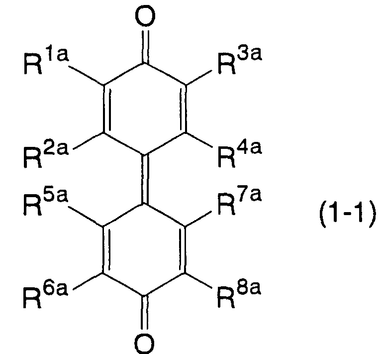
In detail,the above compounds each feature a great reactivity with the inorganic material forming the surface protective layer because a π-electron conjugated system is spread across the molecules thereof so that the compounds has a function to attract particularly a metallic element or carbon of the inorganic material at the initial stage of the film forming process.
Additionally, this function increases the ratio of the molecules of these compounds exposed at the outermost part of the organic photosensitive layer that are combined with the inorganic material to form the nuclei of film growth. This results in a higher density of the binding points at the interface between these layers.
Furthermore, the higher the density of the binding points, the greater the film growth rate. Therefore, the time for film forming process may be reduced thereby minimizing damage on the organic photosensitive layer during the deposition of the surface protective layer by the vapor deposition method or the like.
With a π-bond of a double bond in the molecules split off, each of the above compounds is rigidly combined with a metallic element, carbon or the like via molecular bond. Particularly in the π-bond of the carbonyl group in the compounds of the formulas (1) to (3) or of the A1=C< group (including the carbonyl group) in the compound of the formula (4), there is a great difference of electronegativity between carbon and oxygen or between carbon and the group A1. This provides a dipolar resonance structure wherein carbon has a positive polarity while oxygen or the group A1 has a negative polarity. As a result, the compound is increased in reactivity, contributing to a significant increase in the binding strength between the organic photosensitive layer and the inorganic material.
In addition, each of the compounds has a molecular structure spread in a plane-like fashion as a whole, thus having a great molecular or spatial extent. Furthermore, the compounds are all excellent in compatibility and affinity with the binder resin, presenting a good anchor effect on the binder resin.
Therefore, the binding strength between the organic photosensitive layer and the inorganic material is increased.
According to the invention, the physical stability of the inorganic surface protective layer may be improved by increasing the adhesion thereof to the organic photosensitive layer. Thus, the surface protective layer may be prevented from suffering the occurrence of cracks and delamination in the actual use environment or during the long-term storage. As a result, the electrophotosensitive material featuring a superior durability to the conventional ones may be provided.
Furthermore, the compounds do not produce a deep electric charge trap even when they are changed in the molecular structures thereof due to the molecular bond with a metal or carbon. In addition, the molecular bond occurs only in a limited part of the compound that is exposed at the outermost part of the organic photosensitive layer, so that a major part of the compound in the organic photosensitive layer maintains its initial state as it is. Hence, there is no fear of reducing the photosensitivity of the electrophotosensitive material.
Besides the above merits, all the compounds are excellent in compatibility with the binder resin so that a large amount of each compound may be uniformly dispersed in the binder resin without producing particle aggregation. As a result, the electrophotosensitive material of the invention also features good photosensitivity characteristics.
DETAILED DESCRIPTION OF THE INVENTION
The invention will be described as below.
In an electrophotosensitive material according to the invention, at least an outermost part of an organic photosensitive layer that is in contact with a surface protective layer contains any one of the above compounds represented by the formulas (1) to (4).
Examples of the alkyl group in the above formulas include alkyl groups having 1 to 12 carbon atoms, such as methyl, ethyl, n-propyl (n-Pr), isopropyl (i-Pr), n-butyl (n-Bu), isobutyl (i-Bu), sec-butyl (s-Bu), tert-butyl(t-Bu), pentyl(n-amyl), isopentyl (isoamyl), sec-amyl, tert-amyl, neopentyl, hexyl, heptyl, octyl, nonyl, decyl, undecyl, dodecyl and the like.
Examples of the alkoxy group include alkoxy groups having 1 to 12 carbon atoms, such as methoxy, ethoxy, n-propoxy, isopropoxy, n-butoxy, isobutoxy, sec-butoxy, tert-butoxy, pentyloxy, isopentyloxy, neopentyloxy, hexyloxy, heptyloxy, octyloxy, nonyloxy, decyloxy, undecyloxy, dodecyloxy and the like.
Examples of the aryl group include groups derived from aromatic compounds such as benzene, toluene, xylene, biphenyl, o-terphenyl, m-terphenyl, p-terphenyl, naphthalene, anthracene, phenanthrene, pyrene, indene, azulene, heptalene, biphenylene, fluorene and the like.
Examples of the aralkyl group include aralkyl groups having 4 to 10 carbon atoms in an aryl potion thereof, such as benzyl, benzhydryl, triphenylmethyl, phenethyl, thenyl, furfuryl and the like.
Examples of the alkylthio group include those represented by -S-Ra wherein Ra denotes the above alkyl group having 1 to 12 carbon atoms.
Examples of the aryloxy group include those represented by -O-Φ1 wherein Φ1 denotes the aforesaid aryl group.
Examples of the arylthio group include those represented by -S-Φ2 wherein Φ2 denotes the aforesaid aryl group.
Examples of the alkoxycarbonyl group include those represented by -COORb wherein Rb denotes the above alkyl group having 1 to 12 carbon atoms.
Examples of the cycloalkyl group include cycloalkyl groups having 5 to 12 carbon atoms, such as cyclopentyl, cyclohexyl, 1-cyclohexenyl, cycloheptyl, cyclooctyl, cyclononyl, cyclodecyl, cycloundecyl, cyclododecyl and the like.
Examples of the heterocyclic group include such as thienyl, furyl, pyrrolyl, pyrrolidinyl, oxazoly, isoxazolyl, thiazolyl, isothiazolyl, imidazolyl, 2H-imidazolyl, piperidyl, piperidino, 3-morpholinyl, morpholino and the like. In addition, it may be a heterocyclic group condensed with an aromatic ring.
These groups may be unsubstituted or contain one or more substituents which are exemplified by the above groups and halogen atoms. Other usable substituents include, for example, hydroxyalkyl groups; alkoxyalkyl groups; monoalkyl aminoalkyl groups; dialkyl aminoalkyl groups; halogen-substituted alkyl groups; alkoxycarbonylalkyl groups; carboxyalkyl groups; alkanoyloxyalkyl groups; aminoalkyl groups; amino group; hydroxy group; optionally esterified carboxyl groups; cyano group, nitro group and the like. The substituents are not particularly limited in the position and the number.
Diphenoquinone Derivative
Among the above compounds, an example of a preferred diphenoquinone derivative of the formula (1) includes at least one selected from the group consisting of a diphenoquinone compound represented by a formula (1-1):
Figure 00210001
wherein R1a, R2a, R3a, R4a, R5a, R6a, R7a and R8a are the same or different and each denoting a hydrogen atom, alkyl group, alkoxy group, aryl group, cycloalkyl group or aralkyl group; and
a dinaphthoquinone compound represented by a formula (1-2):
Figure 00220001
wherein R3b, R4b, R5b and R6b are the same or different and each denoting a hydrogen atom, alkyl group, alkoxy group, aryl group, cycloalkyl group or aralkyl group.
Specific examples of the diphenoquinone compound of the formula (1-1) include compounds represented by formulas (1-1-1) to (1-1-32).
Figure 00220002
Figure 00230001
Figure 00230002
Figure 00230003
Figure 00240001
Figure 00240002
Figure 00240003
Figure 00250001
Figure 00250002
Figure 00250003
Figure 00260001
Figure 00260002
Figure 00260003
Figure 00270001
Figure 00270002
Figure 00270003
Specific examples of the dinaphthoquinone compound of the formula (1-2) include compounds represented by formulas (1-2-1) to (1-2-11).
Figure 00280001
Figure 00280002
Figure 00280003
Figure 00290001
Figure 00290002
Figure 00290003
Naphthoquinone Derivative
An example of a preferred naphthoquinone derivative of the formula (2) includes at least one selected from the group consisting of a naphthoquinone compound represented by a formula (2-1):
Figure 00300001
wherein R9a denotes an alkyl group, cycloalkyl group or aryl group;
a naphthoquinone compound represented by a formula (2-2):
Figure 00300002
wherein R9b and R10b are the same or different and each denoting an alkoxy group, alkylthio group, aryloxy group or arylthio group;
a naphthoquinone compound represented by a formula (2-3):
Figure 00300003
wherein R9c denotes an alkyl group or aryl group; and R12c denotes an alkyl group, alkoxy group, aryl group or aryloxy group;
a diindenopyrazine compound represented by a formula (2-4):
Figure 00310001
wherein R11d, R21a and R22a are the same or different and each denoting a hydrogen atom, halogen atom, alkyl group, alkoxy group, aryl group or aralkyl group; 'a' and 'f' are the same or different and each denoting an integer of 0 to 4; and 'g' denotes an integer of 0 to 5;
a diindenopyrazine compound represented by a formula (2-5):
Figure 00310002
wherein R11e and R21b are the same or different and each denoting a hydrogen atom, halogen atom, alkyl group, alkoxy group, aryl group or aralkyl group; and 'a' and 'f' are the same or different and each denoting an integer of 0 to 4; and
a dioxotetracenedione compound represented by a formula (2-6):
Figure 00320001
wherein A5 and A6 are the same or different and each denoting an oxygen atom or =N-CN group; and R23a, R23b, R23c and R23d are the same or different and each denoting a hydrogen atom, alkyl group, alkoxycarbonyl group, cycloalkyl group or group represented by a formula (2-6a):
Figure 00320002
in which R24a, R24b, R24c, R24d and R24e are the same or different and each denoting a hydrogen atom or alkyl group.
Specific examples of the naphthoquinone compound of the formula (2-1) include compounds represented by formulas (2-1-1) to (2-1-6).
Figure 00330001
Figure 00330002
Figure 00330003
Specific examples of the naphthoquinone compound of the formula (2-2) include compounds represented by formulas (2-2-1) to (2-2-23).
Figure 00330004
Figure 00340001
Figure 00340002
Figure 00340003
Figure 00340004
Figure 00350001
Figure 00350002
Figure 00350003
Figure 00360001
Figure 00360002
Figure 00360003
Figure 00360004
Figure 00370001
Figure 00370002
Figure 00370003
Figure 00380001
Figure 00380002
Figure 00380003
Figure 00390001
Figure 00390002
Figure 00390003
Figure 00400001
Figure 00400002
Specific examples of the naphthoquinone compound of the formula (2-3) include compounds represented by formulas (2-3-1) to (2-3-11).
Figure 00400003
Figure 00400004
Figure 00410001
Figure 00410002
Figure 00410003
Figure 00410004
Figure 00410005
Figure 00420001
Figure 00420002
Figure 00420003
Figure 00420004
Specific examples of the diindenopyrazine compound of the formula (2-4) include compounds represented by formulas (2-4-1) to (2-4-4).
Figure 00430001
Figure 00430002
Figure 00430003
Figure 00430004
Specific examples of the diindenopyrazine compound of the formula (2-5) include compounds represented by formulas (2-5-1) to (2-5-4).
Figure 00440001
Figure 00440002
Figure 00440003
Figure 00440004
Specific examples of the dioxotetracenedione compound of the formula (2-6) include compounds represented by formulas (2-6-1) to (2-6-11).
Figure 00450001
Figure 00450002
Figure 00450003
Figure 00450004
Figure 00450005
Figure 00450006
Figure 00460001
Figure 00460002
Figure 00460003
Figure 00460004
Figure 00460005
Naphthylene Diimide Derivative
Specific examples of the naphthylene diimide derivative of the formula (3) include compounds represented by formulas (3-1-1) to (3-1-13).
Figure 00470001
Figure 00470002
Figure 00470003
Figure 00470004
Figure 00470005
Figure 00470006
Figure 00480001
Figure 00480002
Figure 00480003
Figure 00480004
Figure 00480005
Figure 00490001
Figure 00490002
Quinone Derivative
An example of a preferred quinone derivative of the formula (4) includes at least one selected from the group consisting of a compound represented by a formula (4-1):
Figure 00490003
wherein R15a and R18a are the same or different and each denoting a hydrogen atom, halogen atom, alkyl group, alkoxy group, aryl group or aralkyl group; 'b' denotes an integer of 0 to 4, provided that when 'b' is 2 or more, the two groups R15a bonded to adjacent carbon atoms of the ring may be linked together to form a condensed ring jointly with the ring; 'c' denotes an integer of 0 to 5, provided that when 'c' is 2 or more, the groups R18a may be linked together to form a condensed ring jointly with the ring; and A1a denotes an oxygen atom or the group represented by the formula (4a);
a compound represented by a formula (4-2):
Figure 00500001
wherein R15b, R19b and R20b are the same or different and each denoting a hydrogen atom, halogen atom, alkyl group, alkoxy group, aryl group, cycloalkyl group, hetero cyclic group or aralkyl group; 'b', 'd' and 'e' are the same or different and each denoting an integer of 0 to 4, provided that when 'd' is 2 or more, the groups may be linked together to form a condensed ring jointly with the ring; when 'b' or 'e' is 2 or more, the corresponding two groups bonded to adjacent carbon atoms of each ring may be linked together to form a condensed ring jointly with the ring; A1b denotes an oxygen atom or the group represented by the formula (4a); and A4b denotes an oxygen atom or the group represented by the formula (4d); and a compound represented by a formula (4-3):
Figure 00510001
wherein R15c and R18c are the same or different and each denoting a hydrogen atom, halogen atom, alkyl group, alkoxy group, aryl group or aralkyl group; 'b' denotes an integer of 0 to 4, provided that when 'b' is 2 or more, the two groups R15c bonded to adjacent carbon atoms of the ring may be linked together to form a condensed ring jointly with the ring; 'c' denotes an integer of 0 to 5, provided that when 'c' is 2 or more, the groups R18c may be linked together to form a condensed ring jointly with the ring; and A1c denotes an oxygen atom or the group represented by the formula (4a).
Specific examples of the compound of the formula (4-1) include compounds represented by formulas (4-1-1) to (4-1-16).
Figure 00510002
Figure 00520001
Figure 00520002
Figure 00520003
Figure 00520004
Figure 00520005
Figure 00520006
Figure 00530001
Figure 00530002
Figure 00530003
Figure 00530004
Figure 00530005
Figure 00530006
Figure 00540001
Figure 00540002
Figure 00540003
Specific examples of the compound of the formula (4-2) include compounds represented by formulas (4-2-1) to (4-2-20).
Figure 00540004
Figure 00540005
Figure 00550001
Figure 00550002
Figure 00550003
Figure 00550004
Figure 00550005
Figure 00560001
Figure 00560002
Figure 00560003
Figure 00560004
Figure 00560005
Figure 00570001
Figure 00570002
Figure 00570003
Figure 00570004
Figure 00570005
Figure 00580001
Figure 00580002
Figure 00580003
Specific examples of the compound of the formula (4-3) include compounds represented by formulas (4-3-1) to (4-3-15).
Figure 00580004
Figure 00580005
Figure 00590001
Figure 00590002
Figure 00590003
Figure 00590004
Figure 00590005
Figure 00590006
Figure 00600001
Figure 00600002
Figure 00600003
Figure 00600004
Figure 00600005
Figure 00600006
Figure 00610001
The above compounds of the formulas (1) to (4) may be used alone or in combination of two or more types. Organic electrophotosensitive Layer
The organic photosensitive layer includes a single layer type and a multi-layer type, and the invention may be applicable to both of the types.
The single-layer photosensitive layer is formed by the steps of applying a coating solution to a conductive substrate and drying the solution, the coating solution prepared by dissolving or dispersing in a suitable organic solvent, at least one of the compounds of the formulas (1) to (4), the charge generating material, the charge transport material and the binder resin.
The single-layer photosensitive layer features a simple layer construction and good productivity.
Since all the compounds of the formulas (1) to (4) have a function as the electron transport material, the charge transport material may be dispensed with. However, it is preferred to admix the charge transport material in order to attain preferable sensitivity characteristics.
As to the charge transport material, either of the positive-hole transport material and the electron-transport material may be used according to a charge polarity of the photosensitive layer.
Furthermore, both polarities charge transport materials may be used in combination with the above charge transport material. A photosensitive layer including such charge transport materials of opposite polarities is advantageous in that a single layer construction is positively and negatively chargeable.
The multi-layer photosensitive layer is formed by the steps of overlaying on the conductive substrate the charge generating layer containing the charge generating material, applying a coating solution containing the charge transport material and the binder resin onto the resultant charge generating layer, and drying the solution thereby forming the charge transport layer. Otherwise, the multi-layer photosensitive layer may also be obtained by forming the charge transport layer over the conductive substrate, followed by forming thereover the charge generating layer.
The charge generating layer may further contain a charge transport material of the opposite polarity to that of the charge transport layer.
There are a great variety of multi-layer photosensitive layers in correspondence to combinations of the orders of the formation of the charge generating layer and charge transport layer and the polarities of the charge transport materials contained in these layers.
Specific examples of the multi-layer photosensitive layer include the following four types:
  • (a) a negative-charge multi-layer photosensitive layer wherein the charge generating layer containing the charge generating material and, as required, the electron transport material is formed over the conductive substrate and then the charge transport layer containing the positive-hole transport material is laid over the charge generating layer;
  • (b) a negative-charge multi-layer photosensitive layer wherein the charge transport layer containing the electron transport material is formed over the conductive substrate, and then the charge generating layer containing the charge generating material and, as required, the positive-hole transport material is laid over the charge transport layer;
  • (c) a positive-charge multi-layer photosensitive layer wherein the charge generating layer containing the charge generating material and, as required, the positive-hole transport material is formed over the conductive substrate and then, the charge transport layer containing the electron transport material is laid over the charge generating layer; and
  • (d) a positive-charge multi-layer photosensitive layer wherein the charge transport layer containing the positive-hole transport material is formed over the conductive substrate and then, the charge generating layer containing the charge generating material and, as required, the electron transport material is laid over the charge transport layer.
  • As compared with the positive-charge photosensitive layers (c) and (d), the negative-charge photosensitive layers (a) and (b) are generally more preferred because of more excellent electrical characteristics thereof such as photosensitivity and residual potential.
    In addition, the charge generating layer has quite a small thickness as compared with the charge transport layer and hence, the construction (a) with the charge transport layer laid on the upper side is more preferred.
    According to the invention, the upper layer located at the outermost part of the above multi-layer photosensitive layer and contacting the surface protective layer is required to contain at least one of the compounds of the formulas (1) to (4).
    Examples of a usable charge generating material include powders of inorganic photoconductive materials such as selenium, selenium-tellurium, selenium-arsenic, cadmium sulfide, α-silicon and the like; and
    a variety of known pigments including phthalocyanine pigments comprising crystalline phthalocyanine compounds of various crystalline forms such as metal-free phthalocyanine represented by a formula (CG-1):
    Figure 00650001
    titanyl phthalocyanine represented by a formula (CG-2):
    Figure 00650002
    azo pigments, bisazo pigments, perylene pigments, anthanthrone pigments, indigo pigments, triphenylmethane pigments, threne pigments, toluidine pigments, pyrazoline pigments, quinacridone pigments, dithioketopyrolopyrrole pigments and the like.
    The charge generating materials may be used alone or in combination of two or more types such that the photosensitive layer may have sensitivity at a desired wavelength range.
    Particularly, a electrophotosensitive material having photosensitivity in the wavelength range of 700 nm or more is required by digital-optical image forming apparatuses such as laser beam printers, plain paper facsimiles and the like which utilize infrared light such as semiconductor laser beam. Accordingly, phthalocyanine pigments among the above exemplary compounds are preferably employed as the charge generating material.
    Any of the various known electron-transporting compounds may be used as the electron transport material.
    A preferred electron transport material include electron-attracting compounds which include, for example, benzoquinone compounds, diphenoquinone compounds, isatin compounds such as a compound represented by a formula (ET-1):
    Figure 00670001
    naphthoquinone compounds, malononitrile, thiopyran compounds, tetracyanoethylene, 2,4,8-trinitrilothioxanthone, fluorenone compounds such as 2,4,7-trinitrilo-9-fluorenone, dinitrobenzene, dinitroanthracene, dinitroacridine, nitroanthraquinone, succinic anhydride, maleic anhydride, dibromomaleic anhydride, 2,4,7-trinitrofluorenoneimine compounds, ethylated nitrofluorenoneimine compounds, tryptantrin compounds, tryptantrinimine compounds, azafluorenone compounds, dinitropyridoquinazoline compounds, thioxanthene compounds, 2-phenyl-1,4-benzoquinone compounds, 2-phenyl-1,4-naphthoquinone compounds, 5,12-naphthacenequinone compounds, α-cyanostilbene compounds, 4'-nitrostilbene compounds, salts formed by reaction between anionic radicals of benzoquinone compounds and cations.
    These materials may be used alone or in combination of two or more types.
    Any of the various known positive-hole transporting compounds may be used as the positive-hole transport material.
    Examples of a particularly preferred positive-hole transport material include benzidine compounds, phenylenediamine compounds, naphthylenediamine compounds, phenantolylenediamine compounds, oxadiazole compounds such as 2,5-di(4-methylaminophenyl)-1,3,4-oxadiazole, styryl compounds such as 9-(4-diethylaminostyryl)anthracene, carbazole compounds such as poly-N-vinylcarbazole having a repeated unit represented by a formula (HT-1):
    Figure 00680001
    organic polysilane compounds having a repeated unit represented by a formula (HT-2):
    Figure 00680002
    [wherein Ra and Rb are the same or different each denoting an alkyl group, alkoxy group, aryl group or aralkyl group], pyrazoline compounds such as 1-phenyl-3-(p-dimethylaminophenyl)pyrazoline, hydrazone compounds such as diethylaminobenzaldehyde diphenylhydrazone represented by a formula (HT-3):
    Figure 00690001
    triphenylamine compounds such as tris(3-methylphenyl)amine, indole compounds, oxazole compounds, isooxazole compounds, thiazole compounds, thiadiazole compounds, imidazole compounds, pyrazole compounds, triazole compounds, butadiene compounds, pyrene-hydrazone compounds, acrolein compounds, carbazole-hydrazone compounds, quinoline-hydrazone compounds, stilbene-hydrazone compounds, diphenylenediamine compounds and the like.
    These compounds may be used alone or in combination of two or more types.
    Examples of a usable binder resin include thermoplastic resins such as styrene polymers, styrene-butadiene copolymers, styrene-acrylonitrile copolymers, styrene-maleic acid copolymers, acrylic polymers, styrene-acryl copolymers, polyethylene, ethylene-vinyl acetate copolymers, chlorinated polyethylene, polyvinyl chloride, polypropylene, copolymers of vinyl chloride and vinyl acetate, polyester, alkyd resins, polyamide, polyurethane, polycarbonate, polyarylate, polysulfone, diarylphthalate resins, ketone resins, polyvinylbutyral resins, polyether resins and the like;
       crosslinking thermosetting resins such as silicone resins, epoxy resins, phenol resins, urea resins, melamine resins and the like; and
       photosetting resins such as epoxy-acrylate, urethane-acrylate and the like.
    These resins may be used alone or in combination of two or more types.
    Where the aforesaid high-molecular positive-hole transport material such as poly-N-vinylcarbazole or organic polysilane compound is used, such a compound also serves as the binder resin and hence, the aforesaid binder resin may be dispensed with.
    Additionally to the above components, the photosensitive layer may further contain any of the various additives such as fluorene compound, ultraviolet absorber, plasticizer, surfactant, leveling agent and the like. For an increased photosensitivity of the electrophotosensitive material, there may be further added a sensitizer such as terphenyl, halonaphthoquinone, acenaphthylene or the like.
    The single-layer photosensitive layer may preferably contain 0.1 to 50 parts by weight or particularly 0.5 to 30 parts by weight of charge generating material, and 5 to 100 parts by weight or particularly 10 to 80 parts by weight of at least one of the compounds of the formulas (1) to (4), based on 100 parts by weight of binder resin.
    The mixing ratio of the charge transport material may be suitably defined based on the charge polarity or construction of the photosensitive layer.
    Where the positive-hole transport material is used alone as the charge transport material, for instance, the mixing ratio of the positive-hole transport material is preferably in the range of 5 to 500 parts by weight or particularly of 25 to 200 parts by weight based on 100 parts by weight of binder resin. It is also possible to employ the aforesaid positive-hole transport material also serving as the binder resin so as to dispense with the binder resin.
    Where the electron transport material is used alone as the charge transport material, for instance, the mixing ratio of the electron transport material is preferably in the range of 5 to 100 parts by weight or particularly of 10 to 80 parts by weight based on 100 parts by weight of binder resin.
    Where the positive-hole transport material and the electron transport material are used in combination as the charge transport material, for instance, these materials may preferably be present in total amount of 20 to 500 parts by weight or particularly of 30 to 200 parts by weight based on 100 parts by weight of binder resin.
    The single-layer photosensitive layer may preferably have a thickness of 5 to 100 µm or particularly of 10 to 50 µm.
    In the multi-layer photosensitive layer of the construction (a), the charge generating layer disposed on the lower side thereof may be formed from the charge generating material alone or from the binder resin in which the charge generating material and, as required, the electron transport material are dispersed. In the latter case, it is preferred that the charge generating material is present in the range of 5 to 1000 parts by weight or particularly of 30 to 500 parts by weight based on 100 parts by weight of binder resin while the electron transport material is present in the range of 1 to 200 parts by weight or particularly of 5 to 100 parts by weight based on 100 parts by weight of binder resin.
    In the construction (a), the charge transport layer disposed on the upper side may preferably contain the positive-hole transport material in the range of 10 to 500 parts by weight or particularly of 25 to 200 parts by weight based on 100 parts by weight of binder resin, and at least one of the compounds of the formulas (1) to (4) in the range of 0.1 to 250 parts by weight or particularly of 0.5 to 150 parts by weight based on 100 parts by weight of binder resin. In this case, as well, the aforesaid positive-hole transport material also serving as the binder resin may be used so as to dispense with the binder resin.
    As to the thickness of the multi-layer photosensitive layer, the charge generating layer may preferably have a thickness of about 0.01 to 5 µm or particularly of about 0.1 to 3 µm, whereas the charge transport layer may preferably have a thickness of about 2 to 100 µm or particularly of about 5 to 50 µm.
    An intermediate layer or barrier layer may be formed between the single-layer or the multi-layer organic photosensitive layer and the conductive substrate or between the charge generating layer and the charge transport layer of the multi-layer photosensitive layer, so long as such a layer does not decrease the characteristics of the electrophotosensitive material.
    Where each layer forming the electrophotosensitive material is formed by the coating method, the charge generating material, charge transport material, binder resin and the like may be dispersed, by mixing, into an organic solvent using a roll mill, ball mill, attritor, paint shaker, ultrasonic disperser or the like, thereby to prepare a coating solution, which may be applied and dried by the known means.
    Examples of a usable organic solvent include alcohols such as methanol, ethanol, isopropanol, butanol and the like;
  • aliphatic hydrocarbons such as n-hexane, octane, cyclohexane and the like;
  • aromatic hydrocarbons such as benzene, toluene, xylene and the like;
  • halogenated hydrocarbons such as dichloromethane, dichloroethane, carbon tetrachloride, chlorobenzene and the like;
  • ethers such as dimethyl ether, diethyl ether, tetrahydrofuran, 1,4-dioxane, ethyleneglycol dimethyl ether, diethyleneglycol dimethyl ether and the like;
  • ketones such as acetone, methyl ethyl ketone, cyclohexanone and the like;
  • esters such as ethyl acetate, methyl acetate and the like; and
  • dimethylformaldehyde, dimethylformamide, dimethyl sulfoxide and the like. These solvents may be used alone or in combination of two or more types.
  • The coating solution may further contain a surfactant, leveling agent or the like for increasing the dispersibility of the charge generating material and charge transport material, and the surface smoothness of the photosensitive layer.
    Surface Protective Layer
    The inorganic surface protective layer is exemplified by a variety of surface protective layers comprising at least one element selected from the group consisting of metallic elements (the elements on the left side of a line interconnecting boron (B) and astatine (At) in the long-form periodic table) and carbon, or an inorganic compound containing any of these elements.
    The surface protective layer may be formed by any of the various known vapor deposition methods including the chemical vapor deposition methods such as plasma CVD, photo CVD and the like, and the physical vapor deposition methods such as sputtering, vacuum deposition, ion plating and the like.
    In the chemical vapor deposition method such as plasma CVD, there are formed:
  • 1. a film comprising carbon (C) and/or silicon (Si) of the 14-group elements, that is, carbon (C) film, silicon (Si) film or silicon-carbon (Si-C) composite film;
  • 2. a film comprising a compound containing the aforesaid carbon (C) and/or silicon (Si), and at least one element selected from the group consisting of boron (B) and aluminum (Al) of the 13-group elements; nitrogen (Ni) and phosphorus (P) of the 15-group elements; oxygen (O) and sulfur (S) of the 16-group elements; and fluorine (F), chlorine (Cl) and bromine (Br) of the 17-group elements; the film including, for example, silicon-nitrogen (SiN) composite film, silicon-oxygen (SiO) composite film, carbon-fluorine (CF) composite film, carbon-nitrogen (CN) composite film, carbon-boron (CB) composite film, carbon-oxygen (CO) composite film and the like; and
  • 3. a film comprising a compound containing boron (B) and/or aluminum (Al) of the 13-group elements, and at least one element selected from the group consisting of the aforesaid elements including nitrogen (N), phosphorus (P), oxygen (O), sulfur (S), fluorine (F), chlorine (Cl) and bromine (Br), the film including, for example, boron-nitrogen (BN) composite film, aluminum-nitrogen (AlN) composite film and the like.
  • These films may contain a fractional amount of hydrogen (H) for improved electrical characteristics of the surface protective layer.
    In the chemical vapor deposition method, a usable raw material gas for introduction of a constituent element of the surface protective layer include the molecules of the constituent elements, and compounds thereof such as oxides, hydrides, nitrides and halides thereof, the compounds capable of presenting a gaseous state under normal temperature and pressure conditions or of being readily gassified under film forming conditions. As required, these compounds may be diluted with a gas such as hydrogen gas (H2), helium gas, argon gas, neon gas or the like.
    Specific examples of the raw material gas include:
  • silane gas (SiH4) and disilane gas (Si2H6) for silicon introduction;
  • methane gas (CH4), ethane gas (C2H6), propane gas (C3H8) and ethylene gas (C2H4) for carbon introduction;
  • fluorine gas (F2), bromine monofluoride gas (BrF), chlorine difluoride gas (ClF2), carbon tetrafluoride gas (CF4) and silicon tetrafluoride gas (SiF4) for fluorine introduction;
  • nitrogen gas (N2), ammonia gas (NH3), nitrogen oxide gas (NOx) for nitrogen introduction; and
  • boron hydride gas such as diborane gas (B2H6), and tetraborane gas (B4H10) for boron introduction; and the like.
  • Similarly, the. introduction of the other constituent elements may employ compounds capable of presenting a gaseous state under normal temperature and pressure conditions or of being readily gassified under film forming conditions.
    In the physical vapor deposition method, or particularly in the sputtering or ion plating method, there may be formed films, besides the aforesaid films, which each comprise one or more than one metallic elements selected from the group consisting of, for example, gallium (Ga), indium (In) and the like of the 13-group elements; germanium (Ge), tin (Sn), lead (Pb) and the like of the 14-group elements; arsenic (As), antimony (Sb) and the like of the 15-group elements; and selenium (Se) and the like of the 16-group elements, or which each comprise an inorganic compound comprising any of the above metallic elements.
    Preferred as the inorganic surface protective layer are, for example, the carbon (C) film, silicon-carbon (SiC) composite film and the like.
    The thickness of the inorganic surface protective layer may preferably be in the range of 0.01 to 30 µm or particularly of 0.1 to 10 µm.
    The inorganic film defining the surface protective layer may be in any of the amorphous form, microcrystalline form, and crystalline form. Further, the film may comprise a mixture of amorphous and crystalline particles.
    Conductive Substrate
    The conductive substrate may employ substrates formed from various materials having conductivity. Examples of a usable conductive substrate include those formed from metals such as iron, aluminum, copper, tin, platinum, silver, vanadium, molybdenum, chromium, cadmium, titanium, nickel, palladium, indium, stainless steel, brass and the like; those formed from a plastic material on which any of the above metals is deposited or laminated; and glass substrate coated with aluminum iodide, tin oxide, indium oxide or the like.
    In short, the substrate itself may have the conductivity or the surface thereof may have the conductivity. It is preferred that the conductive substrate has a sufficient mechanical strength in use.
    The conductive substrate may have any form, such as sheet, drum and the like, according to the construction of the image forming apparatus to which the conductive substrate is applied.
    EXAMPLES
    The invention will hereinbelow be described by way of reference to examples and comparative examples thereof.
    SINGLE-LAYER ELECTROPHOTOSENSITIVE MATERIAL Example 1-1 Forming Single-Layer Photosensitive Layer
    A ball mill was operated for 50 hours for dispersing by mixing 5 parts by weight of crystalline X-type metal-free phthalocyanine as the charge generating material represented by the formula (CG-1); 100 parts by weight of poly-N-vinylcarbazole (number-average molecular weight Mn=9500) serving as the positive-hole transport material and the binder resin and having the repeated unit represented by the formula (HT-1); and 40 parts by weight of diphenoquinone compound represented by the formula (1-1-1) in 800 parts by weight of tetrahydrofuran, thereby to prepare a coating solution for single-layer photosensitive layer.
    Subsequently, the resultant coating solution was dip coated on an aluminum tube as the conductive substrate and then was air dried at 100°C for 30 minutes. Thus was obtained a single-layer photosensitive layer having a thickness of 25 µm.
    Forming Surface Protective Layer
    The aluminum tube formed with the single-layer photosensitive layer was placed in a chamber of a plasma CVD system. The air within the chamber was evacuated to reach a degree of vacuum of 0.67 Pa while a heater of the system was operated to adjust the temperature of the tube to 50°C.
    Subsequently, methane gas (CH4), silane gas (SiH4) and hydrogen gas (H2) were fed into the chamber at respective flow rates listed below, thereby to adjust the degree of vacuum to 0.47 hPa.
  • Methane gas: 208 SCCM
  • Silane gas: 2.5 SCCM
  • Hydrogen gas: 300 SCCM
  • In this state, a high-frequency electric field having a frequency of 13.56 MHz and an output of 133 W was applied for causing glow discharge in the chamber. The plasma CVD process was performed for depositing an amorphous silicon-carbon (SiC) composite film at a film growth rate of 0.2 µm/hr, thereby laying a surface protective layer having a thickness of 0.5µm over the surface of the single-layer photosensitive layer. Thus was fabricated an electrophotosensitive material of Example 1-1.
    Examples 1-2 to 1-6
    Electrophotosensitive materials of Examples 1-2 to 1-6 were fabricated the same way as in Example 1-1, except that each of the examples used 40 parts by weight of diphenoquinone compound of the formula of a number listed in Table 1.
    Comparative Example 1-1
    An electrophotosensitive material of Comparative Example 1-1 was fabricated the same way as in Example 1-1, except that the diphenoquinone compound was dispensed with.
    Examples 1-7 to 1-12, Comparative Example 1-2
    Electrophotosensitive materials of Examples 1-7 to 1-12 and Comparative Example 1-2 were fabricated the same way as in Examples 1-1 to 1-6 and Comparative Example 1-1, except that the poly-N-vinylcarbazole was replaced by 80 parts by weight of diethylaminobenzaldehyde diphenylhydrazone as the positive-hole transport material represented by the formula (HT-3), and 100 parts by weight of Z-type polycarbonate (weight-average molecular weight Mw=20,000) as the binder resin.
    Photosensitivity Test (I)
    Each of the electrophotosensitive materials of the above examples and comparative examples was charged at +800±20V and the surface potential V0(V) thereof was measured using a drum sensitivity tester available from GENTEC Co.
    A bandpass filter was used to extract monochromatic light from white light from a halogen lamp as a light source of the tester, the monochromatic light having a wavelength of 780 nm and a half width of 20 nm. The surface of the above electrophotosensitive material was irradiated with the monochromatic light at a light intensity of 10 µW/cm2 for 1.0 second while the half-life exposure E1/2 (µJ/cm2) was determined by measuring the time elapsed before the surface potential V0(V) decreased to half. On the other hand, the residual potential Vr(V) was determined by measuring a surface potential after a lapse of 0.5 seconds from the start of the light exposure.
    Durability Test (I)
    The electrophotosensitive materials of the above examples and comparative examples were each mounted in the drum sensitivity tester available from GENTEC Co. The surface of each electrophotosensitive material was charged and exposed to light under the same conditions as in the photosensitivity test (I) and then was exposed to light (wavelength of 660 nm) from an erase lamp of the tester for static elimination. The process of charging, light exposure and static elimination was consecutively repeated in 2,000 cycles with a rotational speed of the electrophotosensitive material set to 40 rpm. Subsequent to the process repeated in cycles, the electrophotosensitive material was subjected to the photosensitivity test (I) again for determining the surface potential V0(V), half-life exposure E1/2 (µJ/cm2) and residual potential Vr(V).
    Solvent Resistance Test
    The adhesion between the surface protective layer and the organic photosensitive layer was examined as follows. A pipette was used to apply methanol dropwise to the surface of each of the electrophotosensitive materials of the examples and comparative examples and changes of surface were visually observed. The solvent resistance of each electrophotosensitive material was evaluated based on the following criteria:
  • ○ : a electrophotosensitive material having a good solvent resistance, suffering no cracks nor delamination of the surface protective layer;
  • Δ: a electrophotosensitive material more or less lower in solvent resistance, suffering cracks spread in the overall surface of the surface protective layer which, however, sustained no delamination; and
  • × : a electrophotosensitive material of an unacceptable solvent resistance, suffering the delamination of the surface protective layer.
  • The results are listed in Table 1.
    Figure 00850001
    It was found from the results of the solvent resistance test listed in the table that the electrophotosensitive material of Comparative Example 1-1 suffered the delamination of the surface protective layer while the electrophotosensitive material of Comparative Example 1-2 sustained cracks. It was thus concluded that where the photosensitive layer does not contain the diphenoquinone compound of the formula (1-1), the effect to improve the physical stability of the inorganic surface protective layer is not obtained.
    It was also found that the electrophotosensitive materials of these comparative examples were significantly decreased in photosensitivity when formed with the surface protective layer, because they presented, in the initial stage, large residual potentials after light exposure and large half-life exposures.
    Furthermore, the electrophotosensitive materials of these comparative examples were found to have poor durability because they were significantly increased in residual potential and half-life exposure after the durability test.
    In contrast, all the electrophotosensitive materials of Examples 1-1 to 1-12 suffered no cracks nor delamination of the surface protective layer in the solvent resistance test. It was thus concluded that the use of the diphenoquinone compound of the formula (1-1) contributed the improvement of the physical stability of the inorganic surface protective layer.
    It was also found that all the electrophotosensitive materials of these examples were free from serious decrease in photosensitivity when formed with the surface protective layer and thus maintained high photosensitivity, because they had small residual potentials after light exposure and half-life exposures.
    In addition, all the electrophotosensitive materials of these examples were free from significant increase in residual potential and half-life exposure after the durability test. Based on this fact and the results of the solvent resistance test, it was concluded that these electrophotosensitive materials achieved greater improvement in durability than the prior-art products.
    Examples 1-13 to 1-24, Comparative Examples 1-3, 1-4
    Electrophotosensitive materials of Examples 1-13 to 1-24 and of Comparative Examples 1-3, 1-4 were fabricated the same way as in Examples 1-1 to 1-12 and Comparative Examples 1-1, 1-2, except that the following procedure was taken to form a surface protective layer of amorphous carbon (C) having a thickness of 0.5µm, instead of the silicon-carbon composite film, over the surface of the single-layer photosensitive layer.
    Forming Surface Protective Layer
    The aluminum tube formed with the single-layer photosensitive layer was placed in the chamber of the plasma CVD system. The air within the chamber was evacuated to reach a degree of vacuum of 0.67 Pa while the heater of the system was operated to adjust the temperature of the tube to 50°C.
    Subsequently, methane gas (CH4) and hydrogen gas (H2) were fed into the chamber at respective flow rates listed below, thereby to adjust the degree of vacuum to 0.47 hPa.
  • Methane gas: 300 SCCM
  • Hydrogen gas: 300 SCCM
  • In this state, a high-frequency electric field having a frequency of 13.56 MHz and an output of 200 W was applied for causing glow discharge in the chamber. The plasma CVD process was performed for depositing a film of amorphous carbon (C) at a film growth rate of 0.15 µm/hr, thereby forming the surface protective layer of the aforesaid thickness over the surface of the single-layer photosensitive layer.
    The electrophotosensitive materials of the above examples and comparative examples were subjected to the same photosensitivity test (I), durability test (I) and solvent resistance test as the above and evaluated for the characteristics thereof. The results are listed in Table 2.
    Figure 00900001
    It was confirmed from the table that if the type of the surface protective layer was changed, the same results as the above were obtained according to the compositions of the single-layer photosensitive layer as the base.
    Specifically, it was found in the solvent resistance test that both the electrophotosensitive materials of Comparative Examples 1-3, 1-4 suffered the delamination of the surface protective layer. It was thus concluded that where the photosensitive layer does not contain the diphenoquinone compound of the formula (1-1), the effect to improve the physical stability of the inorganic surface protective layer is not obtained.
    It was also found that the electrophotosensitive materials of these comparative examples were significantly decreased in photosensitivity when formed with the surface protective layer, because they presented, in the initial stage, large residual potentials after light exposure and large half-life exposures.
    Furthermore, the electrophotosensitive materials of these comparative examples were found to have poor durability because they were significantly increased in residual potential and half-life exposure after the durability test.
    In contrast, all the electrophotosensitive materials of Examples 1-13 to 1-24 suffered no cracks nor delamination of the surface protective layer in the solvent resistance test. It was thus confirmed that the use of the diphenoquinone compound of the formula (1-1) contributed the improvement of the physical stability of the inorganic surface protective layer.
    It was also found that all the electrophotosensitive materials of these examples were free from serious decrease in photosensitivity when formed with the surface protective layer and thus maintained high photosensitivity, because they had small residual potentials after light exposure and half-life exposures.
    In addition, all the electrophotosensitive materials of these examples were free from significant increase in residual potential and half-life exposure after the durability test. Based on this fact and the results of the solvent resistance test, it was concluded that these electrophotosensitive materials achieved greater improvement in durability than the prior-art products.
    Examples 1-25, 1-26, Comparative Example 1-5
    Electrophotosensitive materials of Examples 1-25, 1-26 and of Comparative Example 1-5 were fabricated the same way as in Examples 1-11, 1-12 and Comparative Examples 1-2, except that the following procedure was taken to form a surface protective layer of amorphous silicon-nitrogen (SiN) composite film having a thickness of 0.5µm, instead of the silicon-carbon composite film, over the surface of the single-layer photosensitive layer.
    Forming Surface Protective Layer
    The aluminum tube formed with the single-layer photosensitive layer was placed in the chamber of the plasma CVD system. The air within the chamber was evacuated to reach a degree of vacuum of 0.67 Pa while the heater of the system was operated to adjust the temperature of the tube to 50°C.
    Subsequently, silane gas (SiH4), nitrogen gas (N2) and hydrogen gas (H2) were fed into the chamber at respective flow rates listed below, thereby to adjust the degree of vacuum to 0.47 hPa.
  • Silane gas: 15 SCCM
  • Nitrogen gas: 150 SCCM
  • Hydrogen gas: 75 SCCM
  • In this state, a high-frequency electric field having a frequency of 13.56 MHz and an output of 150 W was applied for causing glow discharge in the chamber. The plasma CVD process was performed for depositing a silicon-nitrogen (SiN) composite film at a film growth rate of 0.75 µm/hr, thereby forming the surface protective layer of the aforesaid thickness over the surface of the single-layer photosensitive layer.
    Examples 1-27, 1-28, Comparative Example 1-6
    Electrophotosensitive materials of Examples 1-27, 1-28 and of Comparative Example 1-6 were fabricated the same way as in Examples 1-11, 1-12 and Comparative Examples 1-2, except that the following procedure was taken to form a surface protective layer of amorphous carbon-nitrogen (CN) composite film having a thickness of 0.5µm, instead of the silicon-carbon composite film, over the surface of the single-layer photosensitive layer.
    Forming Surface Protective Layer
    The aluminum tube formed with the single-layer photosensitive layer was placed in the chamber of the plasma CVD system. The air within the chamber was evacuated to reach a degree of vacuum of 0.67 Pa while the heater of the system was operated to adjust the temperature of the tube to 50°C.
    Subsequently, methane gas (CH4), nitrogen gas (N2) and hydrogen gas (H2) were fed into the chamber at respective flow rates listed below, thereby to adjust the degree of vacuum to 0.47 hPa.
  • Methane gas: 100 SCCM
  • Nitrogen gas: 150 SCCM
  • Hydrogen gas: 100 SCCM
  • In this state, a high-frequency electric field having a frequency of 13.56 MHz and an output of 150 W was applied for causing glow discharge in the chamber. The plasma CVD process was performed for depositing a carbon-nitrogen (CN) composite film at a film growth rate of 0.10 µm/hr, thereby forming the surface protective layer of the aforesaid thickness over the surface of the single-layer photosensitive layer.
    Examples 1-29, 1-30, Comparative Example 1-7
    Electrophotosensitive materials of Examples 1-29, 1-30 and of Comparative Example 1-7 were fabricated the same way as in Examples 1-11, 1-12 and Comparative Examples 1-2, except that the following procedure was taken to form a surface protective layer of amorphous carbon-boron (CB) composite film having a thickness of 0.5µm, instead of the silicon-carbon composite film, over the surface of the single-layer photosensitive layer.
    Forming Surface Protective Layer
    The aluminum tube formed with the single-layer photosensitive layer was placed in the chamber of the plasma CVD system. The air within the chamber was evacuated to reach a degree of vacuum of 0.67 Pa while the heater of the system was operated to adjust the temperature of the tube to 50°C.
    Subsequently, methane gas (CH4), diborane gas (B2H6) and hydrogen gas (H2) were fed into the chamber at respective flow rates listed below, thereby to adjust the degree of vacuum to 0.47 hPa.
  • Methane gas: 100 SCCM
  • Diborane gas: 200 SCCM
  • Hydrogen gas: 100 SCCM
  • In this state, a high-frequency electric field having a frequency of 13.56 MHz and an output of 150 W was applied for causing glow discharge in the chamber. The plasma CVD process was performed for depositing a carbon-boron (CB) composite film at a film growth rate of 0.10 µm/hr, thereby forming the surface protective layer of the aforesaid thickness over the surface of the single-layer photosensitive layer.
    Examples 1-31, 1-32, Comparative Example 1-8
    Electrophotosensitive materials of Examples 1-31, 1-32 and of Comparative Example 1-8 were fabricated the same way as in Examples 1-11, 1-12 and Comparative Examples 1-2, except that the following procedure was taken to form a surface protective layer of amorphous carbon-fluorine (CF) composite film having a thickness of 0.5µm, instead of the silicon-carbon composite film, over the surface of the single-layer photosensitive layer.
    Forming Surface Protective Layer
    The aluminum tube formed with the single-layer photosensitive layer was placed in the chamber of the plasma CVD system. The air within the chamber was evacuated to reach a degree of vacuum of 0.67 Pa while the heater of the system was operated to adjust the temperature of the tube to 50°C.
    Subsequently, methane gas (CH4), carbon tetrafluoride gas (CF4) and hydrogen gas (H2) were fed into the chamber at respective flow rates listed below, thereby to adjust the degree of vacuum to 0.47 hPa.
  • Methane gas: 100 SCCM
  • Carbon tetrafluoride gas: 100 SCCM
  • Hydrogen gas: 100 SCCM
  • In this state, a high-frequency electric field having a frequency of 13.56 MHz and an output of 150 W was applied for causing glow discharge in the chamber. The plasma CVD process was performed for depositing a carbon-fluorine (CF) composite film at a film growth rate of 0.10 µm/hr, thereby forming the surface protective layer of the aforesaid thickness over the surface of the single-layer photosensitive layer.
    Examples 1-33, 1-34, Comparative Example 1-9
    Electrophotosensitive materials of Examples 1-33, 1-34 and of Comparative Example 1-9 were fabricated the same way as in Examples 1-11, 1-12 and Comparative Examples 1-2, except that the following procedure was taken to form a surface protective layer of amorphous boron-nitrogen (BN) composite film having a thickness of 0.5µm, instead of the silicon-carbon composite film, over the surface of the single-layer photosensitive layer.
    Forming Surface Protective Layer
    The aluminum tube formed with the single-layer photosensitive layer was placed in the chamber of the plasma CVD system. The air within the chamber was evacuated to reach a degree of vacuum of 0.67 Pa while the heater of the system was operated to adjust the temperature of the tube to 50°C.
    Subsequently, diborane gas (B2H6), nitrogen gas (N2) and hydrogen gas (H2) were fed into the chamber at respective flow rates listed below, thereby to adjust the degree of vacuum to 0.47 hPa.
  • Diborane gas: 200 SCCM
  • Nitrogen gas: 150 SCCM
  • Hydrogen gas: 150 SCCM
  • In this state, a high-frequency electric field having a frequency of 13.56 MHz and an output of 150 W was applied for causing glow discharge in the chamber. The plasma CVD process was performed for depositing a boron-nitrogen (BN) composite film at a film growth rate of 0.08 µm/hr, thereby forming the surface protective layer of the aforesaid thickness over the surface of the single-layer photosensitive layer.
    The electrophotosensitive materials of the above examples and comparative examples were subjected to the same photosensitivity test (I), durability test (I) and solvent resistance test as the above and evaluated for the characteristics thereof. The results are listed in Table 3.
    Figure 01000001
    It was confirmed from the table that if the type of the surface protective layer was further changed, the same results as the above were obtained according to the compositions of the single-layer photosensitive layer as the base.
    Specifically, it was found from the results of the solvent resistance test that all the electrophotosensitive materials of Comparative Examples 1-7 to 1-9 suffered the delamination of the surface protective layer. The electrophotosensitive materials of Comparative Examples 1-5, 1-6 were found to sustain cracks. It was thus concluded that where the photosensitive layer does not contain the diphenoquinone compound of the formula (1-1), the effect to improve the physical stability of the inorganic surface protective layer is not obtained.
    It was also found that the electrophotosensitive materials of these comparative examples were significantly decreased in photosensitivity when formed with the surface protective layer, because they presented, in the initial stage, large residual potentials after light exposure and large half-life exposures.
    Furthermore, the electrophotosensitive materials of these comparative examples were found to have poor durability because they were significantly increased in residual potential and half-life exposure after the durability test.
    In contrast, all the electrophotosensitive materials of Examples 1-25 to 1-34 suffered no cracks nor delamination of the surface protective layer in the solvent resistance test. It was thus confirmed that the use of the diphenoquinone compound of the formula (1-1) contributed the improvement of the physical stability of the inorganic surface protective layer.
    It was also confirmed that all the electrophotosensitive materials of these examples were free from serious decrease in photosensitivity when formed with the surface protective layer and thus maintained high photosensitivity, because they had small residual potentials after light exposure and half-life exposures.
    In addition, all the electrophotosensitive materials of these examples were free from significant increase in residual potential and half-life exposure after the durability test. Based on this fact and the results of the solvent resistance test, it was concluded that these electrophotosensitive materials achieved greater improvement in durability than the prior-art products.
    MULTI-LAYER ELECTROPHOTOSENSITIVE MATERIAL Example 1-35 Forming Multi-Layer Photosensitive Layer
    The ball mill was operated for dispersing by mixing 2.5 parts by weight of crystalline X-type metal-free phthalocyanine as the charge generating material represented by the formula (CG-1), and 1 part by weight of polyvinylbutyral as the binder resin in 15 parts by weight of tetrahydrofuran, thereby to prepare a coating solution for charge generating layer of the multi-layer photosensitive layer.
    Subsequently, the resultant coating solution was dip coated on the aluminum tube as the conductive substrate and then was air dried at 110°C for 30 minutes. Thus was formed a charge generating layer having a thickness of 0.5 µm.
    The ball mill was operated for dispersing by mixing 1 part by weight of poly-N-vinylcarbazole (number-average molecular weight Mn=9500) serving as the positive-hole transport material and the binder resin and having the repeated unit represented by the formula (HT-1), and 0.2 parts by weight of diphenoquinone compound represented by the formula (1-1-1) in 10 parts by weight of tetrahydrofuran, thereby to prepare a coating solution for charge transport layer of the multi-layer photosensitive layer.
    Subsequently, the resultant coating solution was dip coated on the above charge generating layer and then was air dried at 110°C for 30 minutes, thereby to form a charge transport layer having a thickness of 20 µm. Thus was formed a negative-charge multi-layer photosensitive layer.
    Forming Surface Protective Layer
    The plasma CVD process was performed under the same conditions as in Example 1-1, thereby forming a surface protective layer of amorphous silicon-carbon (SiC) composite film having a thickness of 0.5µm. Thus was fabricated an electrophotosensitive material of Example 1-35.
    Examples 1-36 to 1-40
    Electrophotosensitive materials of Examples 1-36 to 1-40 were fabricated the same way as in Example 1-35 except that each of the examples used 0.2 parts by weight of diphenoquinone compound of the formula of a number listed in Table 4.
    Comparative Example 1-10
    An electrophotosensitive material of Comparative Example 1-10 was fabricated the same way as in Example 1-35 except that the diphenoquinone compound was dispensed with.
    Examples 1-41 to 1-46, Comparative Example 1-11
    Electrophotosensitive materials of Examples 1-41 to 1-46 and Comparative Example 1-11 were fabricated the same way as in Examples 1-35 to 1-40 and Comparative Example 1-10, except that the poly-N-vinylcarbazole was replaced by 0.8 parts by weight of diethylaminobenzaldehyde diphenylhydrazone as the positive-hole transport material represented by the formula (HT-3) and 1 part by weight of Z-type polycarbonate (weight-average molecular weight Mw=20,000) as the binder resin.
    Photosensitivity Test (II)
    Each of the electrophotosensitive materials of the above examples and comparative examples was charged at -800±20V and the surface potential V0(V) thereof was measured using a drum sensitivity tester available from GENTEC Co.
    A bandpass filter was used to extract monochromatic light from white light from a halogen lamp as a light source of the tester, the monochromatic light having a wavelength of 780 nm and a half width of 20 nm. The surface of the above electrophotosensitive material was irradiated with the monochromatic light at a light intensity of 10 µW/cm2 for 1.0 second while the half-life exposure E1/2 (µJ/cm2) was determined by measuring the time elapsed before the surface potential V0(V) decreased to half. On the other hand, the residual potential Vr(V) was determined by measuring a surface potential after a lapse of 0.5 seconds from the start of the light exposure. Durability Test (II)
    The electrophotosensitive materials of the above examples and comparative examples were each mounted in the drum sensitivity tester available from GENTEC Co. The surface of each electrophotosensitive material was charged and exposed to light under the same conditions as in the photosensitivity test (II) and then was exposed to light (wavelength of 660 nm) from an erase lamp of the tester for static elimination. The process of charging, light exposure and static elimination was consecutively repeated in 2,000 cycles with a rotational speed of the electrophotosensitive material set to 40 rpm. Subsequent to the process repeated in cycles, the electrophotosensitive material was subjected to the photosensitivity test (II) again for determining the surface potential V0(V), half-life exposure E1/2 (µJ/cm2) and residual potential Vr(V).
    The results of the above tests as well as those of the aforementioned solvent resistance test are listed in Table 4.
    Figure 01070001
    It was confirmed from the table that if the single-layer photosensitive layer was replaced by the multi-layer photosensitive layer, the same results as the above were obtained according to the compositions of the charge-transport layer defining the outermost part thereof.
    Specifically, it was found in the solvent resistance test that both the electrophotosensitive materials of Comparative Examples 1-10, 1-11 suffered the delamination of the surface protective layer. It was thus concluded that where the photosensitive layer does not contain the diphenoquinone compound of the formula (1-1), the effect to improve the physical stability of the inorganic surface protective layer is not obtained.
    It was also found that the electrophotosensitive materials of these comparative examples were significantly decreased in photosensitivity when formed with the surface protective layer, because they presented, in the initial stage, large residual potentials after light exposure and large half-life exposures.
    Furthermore, the electrophotosensitive materials of these comparative examples were found to have poor durability because they were significantly increased in residual potential and half-life exposure after the durability test.
    In contrast, all the electrophotosensitive materials of Examples 1-35 to 1-46 suffered no cracks nor delamination of the surface protective layer in the solvent resistance test. It was thus confirmed that the use of the diphenoquinone compound of the formula (1-1) contributed the improvement of the physical stability of the inorganic surface protective layer.
    It was also confirmed that all the electrophotosensitive materials of these examples were free from serious decrease in photosensitivity when formed with the surface protective layer and thus maintained high photosensitivity, because they had small residual potentials after light exposure and half-life exposures.
    In addition, all the electrophotosensitive materials of these examples were free from significant increase in residual potential and half-life exposure after the durability test. Based on this fact and the results of the solvent resistance test, it was concluded that these electrophotosensitive materials achieved greater improvement in durability than the prior-art products.
    Examples 1-47 to 1-58, Comparative Examples 1-12, 1-13
    Electrophotosensitive materials of these examples and comparative examples were fabricated the same way as in Examples 1-35 to 1-46 and Comparative Examples 1-10, 1-11, except that the same procedure as in Examples 1-13 to 1-24 and Comparative Examples 1-3, 1-4 was taken to form a surface protective layer of amorphous carbon (C) having a thickness of 0.5µm, instead of the silicon-carbon composite film, over a surface of the multi-layer photosensitive layer.
    The electrophotosensitive materials of the above examples and comparative examples were subjected to the same photosensitivity test (II), durability test (II) and solvent resistance test as the above and were evaluated for the characteristics thereof. The results are listed in Table 5
    Figure 01110001
    It was confirmed from the table that if the type of the surface protective layer was changed, the same results as the above were obtained according to the compositions of the charge-transport layer of the multi-layer photosensitive layer as the base.
    Specifically, it was found in the solvent resistance test that both the electrophotosensitive materials of Comparative Examples 1-12, 1-13 suffered the delamination of the surface protective layer. It was thus concluded that where the photosensitive layer does not contain the diphenoquinone compound of the formula (1-1), the effect to improve the physical stability of the inorganic surface protective layer is not obtained.
    It was also found that the electrophotosensitive materials of these comparative examples were significantly decreased in photosensitivity when formed with the surface protective layer, because they presented, in the initial stage, large residual potentials after light exposure and large half-life exposures.
    Furthermore, the electrophotosensitive materials of these comparative examples were found to have poor durability because they were significantly increased in residual potential and half-life exposure after the durability test.
    In contrast, all the electrophotosensitive materials of Examples 1-47 to 1-58 suffered no cracks nor delamination of the surface protective layer in the solvent resistance test. It was thus confirmed that the use of the diphenoquinone compound of the formula (1-1) contributed the improvement of the physical stability of the inorganic surface protective layer.
    It was also confirmed that all the electrophotosensitive materials of these examples were free from serious decrease in photosensitivity when formed with the surface protective layer and thus maintained high photosensitivity, because they had small residual potentials after light exposure and half-life exposures.
    In addition, all the electrophotosensitive materials of these examples were free from significant increase in residual potential and half-life exposure after the durability test. Based on this fact and the results of the solvent resistance test, it was concluded that these electrophotosensitive materials achieved greater improvement in durability than the prior-art products.
    Examples 1-59, 1-60, Comparative Example 1-14
    Electrophotosensitive materials of these examples and comparative example were fabricated the same way as in Examples 1-45, 1-46 and Comparative Example 1-11, except that the same procedure as in Examples 1-25, 1-26 and Comparative Example 1-5 was taken to form a surface protective layer of amorphous silicon-nitrogen (SiN) composite film having a thickness of 0.5µm, instead of the silicon-carbon composite film, over the surface of the multi-layer photosensitive layer.
    Examples 1-61, 1-62, Comparative Example 1-15
    Electrophotosensitive materials of these examples and comparative example were fabricated the same way as in Examples 1-45, 1-46 and Comparative Example 1-11, except that the same procedure as in Examples 1-27, 1-28 and Comparative Example 1-6 was taken to form a surface protective layer of amorphous carbon-nitrogen (CN) composite film having a thickness of 0.5µm, instead of the silicon-carbon composite film, over the surface of the multi-layer photosensitive layer.
    Examples 1-63, 1-64, Comparative Example 1-16
    Electrophotosensitive materials of these examples and comparative example were fabricated the same way as in Examples 1-45, 1-46 and Comparative Example 1-11, except that the same procedure as in Examples 1-29, 1-30 and Comparative Example 1-7 was taken to form a surface protective layer of amorphous carbon-boron (CB) composite film having a thickness of 0.5µm, instead of the silicon-carbon composite film, over the surface of the multi-layer photosensitive layer.
    Examples 1-65, 1-66, Comparative Example 1-17
    Electrophotosensitive materials of these examples and comparative example were fabricated the same way as in Examples 1-45, 1-46 and Comparative Example 1-11, except that the same procedure as in Examples 1-31, 1-32 and Comparative Example 1-8 was taken to form a surface protective layer of amorphous carbon-fluorine (CF) composite film having a thickness of 0.5µm, instead of the silicon-carbon composite film, over the surface of the multi-layer photosensitive layer.
    Examples 1-67, 1-68, Comparative Example 1-18
    Electrophotosensitive materials of these examples and comparative example were fabricated the same way as in Examples 1-45, 1-46 and Comparative Example 1-11, except that the same procedure as in Examples 1-33, 1-34 and Comparative Example 1-9 was taken to form a surface protective layer of amorphous boron-nitrogen (BN) composite film having a thickness of 0.5µm, instead of the silicon-carbon composite film, over the surface of the multi-layer photosensitive layer.
    The electrophotosensitive materials of the above examples and comparative examples were subjected to the same photosensitivity test (II), durability test (II) and solvent resistance test as the above and were evaluated for the characteristics thereof. The results are listed in Table 6.
    Figure 01170001
    It was confirmed from the table that if the type of the surface protective layer was further changed, the same results as the above were obtained according to the compositions of the charge-transport layer of the multi-layer photosensitive layer as the base.
    Specifically, it was found from the results of the solvent resistance test that both the electrophotosensitive materials of Comparative Examples 1-15 to 1-18 suffered the delamination of the surface protective layer. The electrophotosensitive material of Comparative Example 1-14 was found to sustain cracks. It was thus concluded that where the photosensitive layer does not contain the diphenoquinone compound of the formula (1-1), the effect to improve the physical stability of the inorganic surface protective layer is not obtained.
    It was also found that the electrophotosensitive materials of these comparative examples were significantly decreased in photosensitivity when formed with the surface protective layer, because they presented, in the initial stage, large residual potentials after light exposure and large half-life exposures.
    Furthermore, the electrophotosensitive materials of these comparative examples were found to have poor durability because they were significantly increased in residual potential and half-life exposure after the durability test.
    In contrast, all the electrophotosensitive materials of Examples 1-59 to 1-68 suffered no cracks nor delamination of the surface protective layer in the solvent resistance test. It was thus confirmed that the use of the diphenoquinone compound of the formula (1-1) contributed the improvement of the physical stability of the inorganic surface protective layer.
    It was also confirmed that all the electrophotosensitive materials of these examples were free from serious decrease in photosensitivity when formed with the surface protective layer and thus maintained high photosensitivity, because they had small residual potentials after light exposure and half-life exposures.
    In addition, all the electrophotosensitive materials of these examples were free from significant increase in residual potential and half-life exposure after the durability test. Based on this fact and the results of the solvent resistance test, it was concluded that these electrophotosensitive materials achieved greater improvement in durability than the prior-art products.
    SINGLE-LAYER ELECTROPHOTOSENSITIVE MATERIAL Examples 2-1 to 2-5
    Electrophotosensitive materials of Examples 2-1 to 2-5 were fabricated the same way as in Example 1-1, except that each of the examples used 40 parts by weight of dinaphthoquinone compound of the formula of a number listed in Table 7.
    Examples 2-6 to 2-10
    Electrophotosensitive materials of Examples 2-6 to 2-10 were fabricated the same way as in Example 1-7, except that each of the examples used 40 parts by weight of dinaphthoquinone compound of the formula of a number listed in Table 7.
    The electrophotosensitive materials of the above examples were subjected to the same photosensitivity test (I), durability test (I) and solvent resistance test as the above and were evaluated for the characteristics thereof. The results as well as those of Comparative Examples 1-1, 1-2 are listed in Table 7.
    Figure 01210001
    According to the results of the solvent resistance test, all the electrophotosensitive materials of Examples 2-1 to 2-10 suffered no cracks nor delamination of the surface protective layer. It was thus concluded that the use of the dinaphthoquinone compound of the formula (1-2) contributed the improvement of the physical stability of the inorganic surface protective layer.
    It was also confirmed that all the electrophotosensitive materials of these examples were free from serious decrease in photosensitivity when formed with the surface protective layer and thus maintained high photosensitivity, because they had small residual potentials after light exposure and half-life exposures.
    In addition, all the electrophotosensitive materials of these examples were free from significant increase in residual potential and half-life exposure after the durability test. Based on this fact and the results of the solvent resistance test, it was concluded that these electrophotosensitive materials achieved greater improvement in durability than the prior-art products.
    Examples 2-11 to 2-20
    Electrophotosensitive materials of Examples 2-11 to 2-20 were fabricated the same way as in Examples 2-1 to 2-10, except that the same procedure as in Examples 1-13 to 1-24 was taken to form a surface protective layer of amorphous carbon (C) having a thickness of 0.5µm, instead of the silicon-carbon composite film, over the surface of the single-layer photosensitive layer.
    The electrophotosensitive materials of these examples were subjected to the same photosensitivity test (I), durability test (I) and solvent resistance test as the above and were evaluated for the characteristics thereof. The results as well as those of Comparative Examples 1-3, 1-4 are listed in Table 8.
    Figure 01240001
    It was confirmed from the table that if the type of the surface protective layer was changed, the same results as the above were obtained according to the compositions of the single-layer photosensitive layer as the base.
    Specifically, it was found from the results of the solvent resistance test that all the electrophotosensitive materials of Examples 2-11 to 2-20 suffered no cracks nor delamination of the surface protective layer. It was thus confirmed that the use of the dinaphthoquinone compound of the formula (1-2) contributed the improvement of the physical stability of the inorganic surface protective layer.
    It was also confirmed that all the electrophotosensitive materials of these examples were free from serious decrease in photosensitivity when formed with the surface protective layer and thus maintained high photosensitivity, because they had small residual potentials after light exposure and half-life exposures.
    In addition, all the electrophotosensitive materials of these examples were free from significant increase in residual potential and half-life exposure after the durability test. Based on this fact and the results of the solvent resistance test, it was concluded that these electrophotosensitive materials achieved greater improvement in durability than the prior-art products.
    Examples 2-21, 2-22
    Electrophotosensitive materials of Examples 2-21, 2-22 were fabricated the same way as in Examples 2-7, 2-8 except that the same procedure as in Examples 1-25, 1-26 was taken to form a surface protective layer of amorphous silicon-nitrogen (SiN) composite film having a thickness of 0.5µm, instead of the silicon-carbon composite film, over the surface of the single-layer photosensitive layer.
    Examples 2-23, 2-24
    Electrophotosensitive materials of Examples 2-23, 2-24 were fabricated the same way as in Examples 2-7, 2-8 except that the same procedure as in Examples 1-27, 1-28 was taken to form a surface protective layer of amorphous carbon-nitrogen (CN) composite film having a thickness of 0.5µm, instead of the silicon-carbon composite film, over the surface of the single-layer photosensitive layer.
    Examples 2-25, 2-26
    Electrophotosensitive materials of Examples 2-25, 2-26 were fabricated the same way as in Examples 2-7, 2-8 except that the same procedure as in Examples 1-29, 1-30 was taken to form a surface protective layer of amorphous carbon-boron (CB) composite film having a thickness of 0.5µm, instead of the silicon-carbon composite film, over the surface of the single-layer photosensitive layer.
    Examples 2-27, 2-28
    Electrophotosensitive materials of Examples 2-27, 2-28 were fabricated the same way as in Examples 2-7, 2-8 except that the same procedure as in Examples 1-31, 1-32 was taken to form a surface protective layer of amorphous carbon-fluorine (CF) composite film having a thickness of 0.5µm, instead of the silicon-carbon composite film, over the surface of the single-layer photosensitive layer.
    Examples 2-29, 2-30
    Electrophotosensitive materials of Examples 2-29, 2-30 were fabricated the same way as in Examples 2-7, 2-8 except that the same procedure as in Examples 1-33, 1-34 was taken to form a surface protective layer of amorphous boron-nitrogen (BN) composite film having a thickness of 0.5µm, instead of the silicon-carbon composite film, over the surface of the single-layer photosensitive layer.
    The electrophotosensitive materials of the above examples were subjected to the same photosensitivity test (I), durability test (I) and solvent resistance test as the above and were evaluated for the characteristics thereof. The results as well as those of Comparative Examples 1-5 to 1-9 are listed in Table 9.
    Figure 01290001
    It was confirmed from the table that if the type of the surface protective layer was further changed, the same results as the above were obtained according to the compositions of the single-layer photosensitive layer as the base.
    According to the results of the solvent resistance test listed in the table, all the electrophotosensitive materials of Examples 2-21 to 2-30 suffered no cracks nor delamination of the surface protective layer. It was thus concluded that the use of the dinaphthoquinone compound of the formula (1-2) contributed the improvement of the physical stability of the inorganic surface protective layer.
    It was also confirmed that all the electrophotosensitive materials of these examples were free from serious decrease in photosensitivity when formed with the surface protective layer and thus maintained high photosensitivity, because they had small residual potentials after light exposure and half-life exposures.
    In addition, all the electrophotosensitive materials of these examples were free from significant increase in residual potential and half-life exposure after the durability test. Based on this fact and the results of the solvent resistance test, it was concluded that these electrophotosensitive materials achieved greater improvement in durability than the prior-art products.
    MULTI-LAYER ELECTROPHOTOSENSITIVE MATERIAL Examples 2-31 to 2-35
    Electrophotosensitive materials of Examples 2-31 to 2-35 were fabricated the same way as in Example 1-35, except that each of the examples used 0.2 parts by weight of dinaphthoquinone compound of the formula of a number listed in Table 10.
    Examples 2-36 to 2-40
    Electrophotosensitive materials of Examples 2-36 to 2-40 were fabricated the same way as in Example 1-41, except that each of the examples used 40 parts by weight of dinaphthoquinone compound of the formula of a number listed in Table 10.
    The electrophotosensitive materials of the above examples were subjected to the same sensitivity test (II), durability test (II) and solvent resistance test as the above and evaluated for the characteristics thereof. The results as well as those of Comparative Examples 1-10, 1-11 are listed in Table 10.
    Figure 01320001
    It was confirmed from the table that if the single-layer photosensitive layer was replaced by the multi-layer photosensitive layer, the same results as the above were obtained according to the compositions of the charge transport layer defining the outermost part thereof.
    According to the results of the solvent resistance test listed in the table, all the electrophotosensitive materials of Examples 2-31 to 2-40 suffered no cracks nor delamination of the surface protective layer. It was thus concluded that the use of the dinaphthoquinone compound of the formula (1-2) contributed the improvement of the physical stability of the inorganic surface protective layer.
    It was also confirmed that all the electrophotosensitive materials of these examples were free from serious decrease in photosensitivity when formed with the surface protective layer and thus maintained high photosensitivity, because they had small residual potentials after light exposure and half-life exposures.
    In addition, all the electrophotosensitive materials of these examples were free from significant increase in residual potential and half-life exposure after the durability test. Based on this fact and the results of the solvent resistance test, it was concluded that these electrophotosensitive materials achieved greater improvement in durability than the prior-art products.
    Examples 2-41 to 2-50
    Electrophotosensitive materials of these examples were fabricated the same way as in Examples 2-31 to 2-40, except that the same procedure as in Examples 1-13 to 1-24 was taken to form a surface protective layer of amorphous carbon (C) having a thickness of 0.5µm, instead of the silicon-carbon composite film, over a surface of the multi-layer photosensitive layer.
    The electrophotosensitive materials of these examples were subjected to the same photosensitivity test (II), durability test (II) and solvent resistance test as the above and were evaluated for the characteristics thereof. The results as well as those of Comparative Examples 1-12, 1-13, are listed in Table 11.
    Figure 01350001
    It was confirmed from the table that if the type of the surface protective layer was changed, the same results as the above were obtained according to the compositions of the charge transport layer of the multi-layer photosensitive layer as the base.
    According to the results of the solvent resistance test listed in the table, all the electrophotosensitive materials of Examples 2-41 to 2-50 suffered no cracks nor delamination of the surface protective layer. It was thus concluded that the use of the dinaphthoquinone compound of the formula (1-2) contributed the improvement of the physical stability of the inorganic surface protective layer.
    It was also confirmed that all the electrophotosensitive materials of these examples were free from serious decrease in photosensitivity when formed with the surface protective layer and thus maintained high photosensitivity, because they had small residual potentials after light exposure and half-life exposures.
    In addition, all the electrophotosensitive materials of these examples were free from significant increase in residual potential and half-life exposure after the durability test. Based on this fact and the results of the solvent resistance test, it was concluded that these electrophotosensitive materials achieved greater improvement in durability than the prior-art products.
    Examples 2-51 to 2-52
    Electrophotosensitive materials of these examples were fabricated the same way as in Examples 2-37, 2-38 except that the same procedure as in Examples 1-25, 1-26 was taken to form a surface protective layer of amorphous silicon-nitrogen (SiN) composite film having a thickness of 0.5µm, instead of the silicon-carbon composite film, over the surface of the multi-layer photosensitive layer.
    Examples 2-53, 2-54
    Electrophotosensitive materials of these examples were fabricated the same way as in Examples 2-37, 2-38 except that the same procedure as in Examples 1-27, 1-28 was taken to form a surface protective layer of amorphous carbon-nitrogen (CN) composite film having a thickness of 0.5µm, instead of the silicon-carbon composite film, over the surface of the multi-layer photosensitive layer.
    Examples 2-55, 2-56
    Electrophotosensitive materials of these examples were fabricated the same way as in Examples 2-37, 2-38 except that the same procedure as in Examples 1-29, 1-30 was taken to form a surface protective layer of amorphous carbon-boron (CB) composite film having a thickness of 0.5µm, instead of the silicon-carbon composite film, over the surface of the multi-layer photosensitive layer.
    Examples 2-57, 2-58
    Electrophotosensitive materials of these examples were fabricated the same way as in Examples 2-37, 2-38 except that the same procedure as in Examples 1-31, 1-32 was taken to form a surface protective layer of amorphous carbon-fluorine (CF) composite film having a thickness of 0.5µm, instead of the silicon-carbon composite film, over the surface of the multi-layer photosensitive layer.
    Examples 2-59, 2-60
    Electrophotosensitive materials of these examples were fabricated the same way as in Examples 2-37, 2-38 except that the same procedure as in Examples 1-33, 1-34 was taken to form a surface protective layer of amorphous boron-nitrogen (BN) composite film having a thickness of 0.5µm, instead of the silicon-carbon composite film, over the surface of the multi-layer photosensitive layer.
    The electrophotosensitive materials of the above examples were subjected to the same photosensitivity test (II), durability test (II) and solvent resistance test as the above and were evaluated for the characteristics thereof. The results as well as those of Comparative Examples 1-14 to 1-18 are listed in Table 12.
    Figure 01400001
    It was confirmed from the table that if the type of the surface protective layer was further changed, the same results as the above were obtained according to the compositions of the charge transport layer of the multi-layer photosensitive layer as the base.
    According to the results of the solvent resistance test listed in the table, all the electrophotosensitive materials of Examples 2-51 to 2-60 suffered no cracks nor delamination of the surface protective layer. It was thus concluded that the use of the dinaphthoquinone compound of the formula (1-2) contributed the improvement of the physical stability of the inorganic surface protective layer.
    It was also confirmed that all the electrophotosensitive materials of these examples were free from serious decrease in photosensitivity when formed with the surface protective layer and thus maintained high photosensitivity, because they had small residual potentials after light exposure and half-life exposures.
    In addition, all the electrophotosensitive materials of these examples were free from significant increase in residual potential and half-life exposure after the durability test. Based on this fact and the results of the solvent resistance test, it was concluded that these electrophotosensitive materials achieved greater improvement in durability than the prior-art products.
    SINGLE-LAYER ELECTROPHOTOSENSITIVE MATERIAL Examples 3-1 to 3-7
    Electrophotosensitive materials of Examples 3-1 to 3-7 were fabricated the same way as in Example 1-1, except that each of the examples used 40 parts by weight of naphthoquinone compound of the formula of a number listed in Table 13.
    Examples 3-8 to 3-14
    Electrophotosensitive materials of Examples 3-8 to 3-14 were fabricated the same way as in Example 1-7, except that each of the examples used 40 parts by weight of naphthoquinone compound of the formula of a number listed in Table 13.
    The electrophotosensitive materials of the above examples were subjected to the same photosensitivity test (I), durability test (I) and solvent resistance test as the above and were evaluated for the characteristics thereof. The results as well as those of Comparative Examples 1-1, 1-2 are listed in Table 13.
    Figure 01430001
    According to the results of the solvent resistance test listed in the table, all the electrophotosensitive materials of Examples 3-1 to 3-14 suffered no cracks nor delamination of the surface protective layer. It was thus concluded that the use of the naphthoquinone compounds of the formulas (2-1) to (2-3) contributed the improvement of the physical stability of the inorganic surface protective layer.
    It was also confirmed that all the electrophotosensitive materials of these examples were free from serious decrease in photosensitivity when formed with the surface protective layer and thus maintained high photosensitivity, because they had small residual potentials after light exposure and half-life exposures.
    In addition, all the electrophotosensitive materials of these examples were free from significant increase in residual potential and half-life exposure after the durability test. Based on this fact and the results of the solvent resistance test, it was concluded that these electrophotosensitive materials achieved greater improvement in durability than the prior-art products.
    Examples 3-15 to 3-28
    Electrophotosensitive materials of Examples 3-15 to 3-28 were fabricated the same way as in Examples 3-1 to 3-14 except that the same procedure as in Examples 1-13 to 1-24 was taken to form a surface protective layer of amorphous carbon (C) having a thickness of 0.5µm, instead of the silicon-carbon composite film, over the surface of the single-layer photosensitive layer.
    The electrophotosensitive materials of the above examples were subjected to the same photosensitivity test (I), durability test (I) and solvent resistance test as the above and were evaluated for the characteristics thereof. The results as well as those of Comparative Examples 1-3, 1-4 are listed in Table 14.
    Figure 01460001
    It was confirmed from the table that if the type of the surface protective layer was changed, the same results as the above were obtained according to the compositions of the single-layer photosensitive layer as the base.
    According to the results of the solvent resistance test listed in the table, all the electrophotosensitive materials of Examples 3-15 to 3-28 suffered no cracks nor delamination of the surface protective layer. It was thus concluded that the use of the naphthoquinone compounds of the formulas (2-1) to (2-3) contributed the improvement of the physical stability of the inorganic surface protective layer.
    It was also confirmed that all the electrophotosensitive materials of these examples were free from serious decrease in photosensitivity when formed with the surface protective layer and thus maintained high photosensitivity, because they had small residual potentials after light exposure and half-life exposures.
    In addition, all the electrophotosensitive materials of these examples were free from significant increase in residual potential and half-life exposure after the durability test. Based on this fact and the results of the solvent resistance test, it was concluded that these electrophotosensitive materials achieved greater improvement in durability than the prior-art products.
    Examples 3-29 to 3-32
    Electrophotosensitive materials of Examples 3-29 to 3-32 were fabricated the same way as in Examples 3-8, 3-10, 3-12 and 3-13 except that the same procedure as in Examples 1-25, 1-26 was taken to form a surface protective layer of amorphous silicon-nitrogen (SiN) composite film having a thickness of 0.5µm, instead of the silicon-carbon composite film, over the surface of the single-layer photosensitive layer.
    Examples 3-33 to 3-36
    Electrophotosensitive materials of Examples 3-33 to 3-36 were fabricated the same way as in Examples 3-8, 3-10, 3-12 and 3-13 except that the same procedure as in Examples 1-27, 1-28 was taken to form a surface protective layer of amorphous carbon-nitrogen (CN) composite film having a thickness of 0.5µm, instead of the silicon-carbon composite film, over the surface of the single-layer photosensitive layer.
    Examples 3-37 to 3-40
    Electrophotosensitive materials of Examples 3-37 to 3-40 were fabricated the same way as in Examples 3-8, 3-10, 3-12 and 3-13 except that the same procedure as in Examples 1-29, 1-30 was taken to form a surface protective layer of amorphous carbon-boron (CB) composite film having a thickness of 0.5µm, instead of the silicon-carbon composite film, over the surface of the single-layer photosensitive layer.
    Examples 3-41 to 3-44
    Electrophotosensitive materials of Examples 3-41 to 3-44 were fabricated the same way as in Examples 3-8, 3-10, 3-12 and 3-13 except that the same procedure as in Examples 1-31, 1-32 was taken to form a surface protective layer of amorphous carbon-fluorine (CF) composite film having a thickness of 0.5µm, instead of the silicon-carbon composite film, over the surface of the single-layer photosensitive layer.
    Examples 3-45 to 3-48
    Electrophotosensitive materials of Examples 3-45 to 3-48 were fabricated the same way as in Examples 3-8, 3-10, 3-12 and 3-13 except that the same procedure as in Examples 1-33, 1-34 was taken to form a surface protective layer of amorphous boron-nitrogen (BN) composite film having a thickness of 0.5µm, instead of the silicon-carbon composite film, over the surface of the single-layer photosensitive layer.
    The electrophotosensitive materials of the above examples were subjected to the same photosensitivity test (I), durability test (I) and solvent resistance test as the above and were evaluated for the characteristics thereof. The results as well as those of Comparative Examples 1-5 to 1-9 are listed in Tables 15a and 15b.
    Figure 01510001
    Figure 01520001
    It was confirmed from the tables that if the type of the surface protective layer was further changed, the same results as the above were obtained according to the compositions of the single-layer photosensitive layer as the base.
    According to the results of the solvent resistance test listed in the tables, all the electrophotosensitive materials of Examples 3-29 to 3-48 suffered no cracks nor delamination of the surface protective layer. It was thus concluded that the use of the naphthoquinone compounds of the formulas (2-1) to (2-3) contributed the improvement of the physical stability of the inorganic surface protective layer.
    It was also confirmed that all the electrophotosensitive materials of these examples were free from serious decrease in photosensitivity when formed with the surface protective layer and thus maintained high photosensitivity, because they had small residual potentials after light exposure and half-life exposures.
    In addition, all the electrophotosensitive materials of these examples were free from significant increase in residual potential and half-life exposure after the durability test. Based on this fact and the results of the solvent resistance test, it was concluded that these electrophotosensitive materials achieved greater improvement in durability than the prior-art products.
    MULTI-LAYER ELECTROPHOTOSENSITIVE MATERIAL Examples 3-49 to 3-55
    Electrophotosensitive materials of Examples 3-49 to 3-55 were fabricated the same way as in Example 1-35, except that each of the examples used 0.2 parts by weight of naphthoquinone compound of the formula of a number listed in Table 16.
    Examples 3-56 to 3-62
    Electrophotosensitive materials of Examples 3-56 to 3-62 were fabricated the same way as in Example 1-41, except that each of the examples used 40 parts by weight of naphthoquinone compound of the formula of a number listed in Table 16.
    The electrophotosensitive materials of the above examples were subjected to the same photosensitivity test (II), durability test (II) and solvent resistance test as the above and were evaluated for the characteristics thereof. The results as well as the those of Comparative Examples 1-10, 1-11 are listed in Table 16.
    Figure 01550001
    It was confirmed from the table that if the single-layer photosensitive layer was replaced by the multi-layer photosensitive layer, the same results as the above were obtained according to the compositions of the charge transport layer defining the outermost part thereof.
    According to the results of the solvent resistance test listed in the table, all the electrophotosensitive materials of Examples 3-49 to 3-62 suffered no cracks nor delamination of the surface protective layer. It was thus concluded that the use of the naphthoquinone compounds of the formulas (2-1) to (2-3) contributed the improvement of the physical stability of the inorganic surface protective layer.
    It was also confirmed that all the electrophotosensitive materials of these examples were free from serious decrease in photosensitivity when formed with the surface protective layer and thus maintained high photosensitivity, because they had small residual potentials after light exposure and half-life exposures.
    In addition, all the electrophotosensitive materials of these examples were free from significant increase in residual potential and half-life exposure after the durability test. Based on this fact and the results of the solvent resistance test, it was concluded that these electrophotosensitive materials achieved greater improvement in durability than the prior-art products.
    Examples 3-63 to 3-76
    Electrophotosensitive materials of these examples were fabricated the same way as in Examples 3-49 to 3-62 except that the same procedure as in Examples 1-13 to 1-24 was taken to form a surface protective layer of amorphous carbon (C) having a thickness of 0.5µm, instead of the silicon-carbon composite film, over the surface of the multi-layer photosensitive layer.
    The electrophotosensitive materials of the above examples were subjected to the same photosensitivity test (II), durability test (II) and solvent resistance test as the above and were evaluated for the characteristics thereof. The results as well as those of Comparative Examples 1-12, 1-13 are listed in Table 17.
    Figure 01580001
    It was confirmed from the table that if the type of the surface protective layer was changed, the same results as the above were obtained according to the compositions of the charge transport layer of the multi-layer photosensitive layer as the base.
    According to the results of the solvent resistance test listed in the table, all the electrophotosensitive materials of Examples 3-63 to 3-76 suffered no cracks nor delamination of the surface protective layer. It was thus concluded that the use of the naphthoquinone compounds of the formulas (2-1) to (2-3) contributed the improvement of the physical stability of the inorganic surface protective layer.
    It was also confirmed that all the electrophotosensitive materials of these examples were free from serious decrease in photosensitivity when formed with the surface protective layer and thus maintained high photosensitivity, because they had small residual potentials after light exposure and half-life exposures.
    In addition, all the electrophotosensitive materials of these examples were free from significant increase in residual potential and half-life exposure after the durability test. Based on this fact and the results of the solvent resistance test, it was concluded that these electrophotosensitive materials achieved greater improvement in durability than the prior-art products.
    Examples 3-77 to 3-80
    Electrophotosensitive materials of these examples were fabricated the same way as in Examples 3-56, 3-58, 3-60 and 3-61 except that the same procedure as in Examples 1-25, 1-26 was taken to form a surface protective layer of amorphous silicon-nitrogen (SiN) composite film having a thickness of 0.5µm, instead of the silicon-carbon composite film, over the surface of the multi-layer photosensitive layer.
    Examples 3-81 to 3-84
    Electrophotosensitive materials of these examples were fabricated the same way as in Examples 3-56, 3-58, 3-60 and 3-61 except that the same procedure as in Examples 1-27, 1-28 was taken to form a surface protective layer of amorphous carbon-nitrogen (CN) composite film having a thickness of 0.5µm, instead of the silicon-carbon composite film, over the surface of the multi-Layer photosensitive layer.
    Examples 3-85 to 3-88
    Electrophotosensitive materials of these examples were fabricated the same way as in Examples 3-56, 3-58, 3-60 and 3-61 except that the same procedure as in Examples 1-29, 1-30 was taken to form a surface protective layer of amorphous carbon-boron (CB) composite film having a thickness of 0.5µm, instead of the silicon-carbon composite film, over the surface of the multi-layer photosensitive layer.
    Examples 3-89 to 3-92
    Electrophotosensitive materials of these examples were fabricated the same way as in Examples 3-56, 3-58, 3-60 and 3-61 except that the same procedure as in Examples 1-31, 1-32 was taken to form a surface protective layer of amorphous carbon-fluorine (CF) composite film having a thickness of 0.5µm, instead of the silicon-carbon composite film, over the surface of the multi-layer photosensitive layer.
    Examples 3-93 to 3-96
    Electrophotosensitive materials of these examples were fabricated the same way as in Examples 3-56, 3-58, 3-60 and 3-61 except that the same procedure as in Examples 1-33, 1-34 was taken to form a surface protective layer of amorphous boron-nitrogen (BN) composite film having a thickness of 0.5µm, instead of the silicon-carbon composite film, over the surface of the multi-layer photosensitive layer.
    The electrophotosensitive materials of the above examples were subjected to the same photosensitivity test (II), durability test (II) and solvent resistance test as the above and were evaluated for the characteristics thereof. The results as well as those of Comparative Examples 1-14 to 1-18 are listed in Tables 18a, 18b.
    Figure 01630001
    Figure 01640001
    It was confirmed from the tables that if the type of the surface protective layer was further changed, the same results as the above were obtained according to the compositions of the charge transport layer of the multi-layer photosensitive layer as the base.
    According to the results of the solvent resistance test listed in the table, all the electrophotosensitive materials of Examples 3-77 to 3-96 suffered no cracks nor delamination of the surface protective layer. It was thus concluded that the use of the naphthoquinone compounds of the formulas (2-1) to (2-3) contributed the improvement of the physical stability of the inorganic surface protective layer.
    It was also confirmed that all the electrophotosensitive materials of these examples were free from serious decrease in photosensitivity when formed with the surface protective layer and thus maintained high photosensitivity, because they had small residual potentials after light exposure and half-life exposures.
    In addition, all the electrophotosensitive materials of these examples were free from significant increase in residual potential and half-life exposure after the durability test. Based on this fact and the results of the solvent resistance test, it was concluded that these electrophotosensitive materials achieved greater improvement in durability than the prior-art products.
    SINGLE-LAYER ELECTROPHOTOSENSITIVE MATERIAL Examples 4-1 to 4-4
    Electrophotosensitive materials of Examples 4-1 to 4-4 were fabricated the same way as in Example 1-1 except that each of the examples used 40 parts by weight of diindenopyrazine compound of the formula of a number listed in Table 19.
    Examples 4-5 to 4-8
    Electrophotosensitive materials of Examples 4-5 to 4-8 were fabricated the same way as in Example 1-7 except that each of the examples used 40 parts by weight of diindenopyrazine compound of the formula of a number listed in Table 19.
    The electrophotosensitive materials of the above examples were subjected to the same photosensitivity test (I), durability test (I) and solvent resistance test as the above and were evaluated for the characteristics thereof. The results as well as those of Comparative Examples 1-1, 1-2 are listed in Table 19.
    Figure 01670001
    According to the results of the solvent resistance test listed in the table, all the electrophotosensitive materials of Examples 4-1 to 4-8 suffered no cracks nor delamination of the surface protective layer. It was thus concluded that the use of the diindenopyrazine compounds of the formulas (2-4), (2-5) contributed the improvement of the physical stability of the inorganic surface protective layer.
    It was also confirmed that all the electrophotosensitive materials of these examples were free from serious decrease in photosensitivity when formed with the surface protective layer and thus maintained high photosensitivity, because they had small residual potentials after light exposure and half-life exposures.
    In addition, all the electrophotosensitive materials of these examples were free from significant increase in residual potential and half-life exposure after the durability test. Based on this fact and the results of the solvent resistance test, it was concluded that these electrophotosensitive materials achieved greater improvement in durability than the prior-art products.
    Examples 4-9 to 4-16
    Electrophotosensitive materials of Examples 4-9 to 4-16 were fabricated the same way as in Examples 4-1 to 4-8 except that the same procedure as in Examples 1-13 to 1-24 was taken to form a surface protective layer of amorphous carbon (C) having a thickness of 0.5µm, instead of the silicon-carbon composite film, over the surface of the single-layer photosensitive layer.
    The electrophotosensitive materials of the above examples were subjected to the same photosensitivity test (I), durability test (I) and solvent resistance test as the above and were evaluated for the characteristics thereof. The results as well as those of Comparative Examples 1-3, 1-4 are listed in Table 20.
    Figure 01700001
    It was confirmed from the table that if the type of the surface protective layer was changed, the same results as the above were obtained according to the compositions of the single-layer photosensitive layer as the base.
    According to the results of the solvent resistance test listed in the table, all the electrophotosensitive materials of Examples 4-9 to 4-16 suffered no cracks nor delamination of the surface protective layer. It was thus concluded that the use of the diindenopyrazine compounds of the formulas (2-4), (2-5) contributed the improvement of the physical stability of the inorganic surface protective layer.
    It was also confirmed that all the electrophotosensitive materials of these examples were free from serious decrease in photosensitivity when formed with the surface protective layer and thus maintained high photosensitivity, because they had small residual potentials after light exposure and half-life exposures.
    In addition, all the electrophotosensitive materials of these examples were free from significant increase in residual potential and half-life exposure after the durability test. Based on this fact and the results of the solvent resistance test, it was concluded that these electrophotosensitive materials achieved greater improvement in durability than the prior-art products.
    Examples 4-17, 4-18
    Electrophotosensitive materials of Examples 4-17, 4-18 were fabricated the same way as in Examples 4-5, 4-8 except that the same procedure as in Examples 1-25, 1-26 was taken to form a surface protective layer of amorphous silicon-nitrogen (SiN) composite film having a thickness of 0.5µm, instead of the silicon-carbon composite film, over the surface of the single-layer photosensitive layer.
    Examples 4-19, 4-20
    Electrophotosensitive materials of Examples 4-19, 4-20 were fabricated the same way as in Examples 4-5, 4-8 except that the same procedure as in Examples 1-27, 1-28 was taken to form a surface protective layer of amorphous carbon-nitrogen (CN) composite film having a thickness of 0.5µm, instead of the silicon-carbon composite film, over the surface of the single-layer photosensitive layer.
    Examples 4-21, 4-22
    Electrophotosensitive materials of Examples 4-21, 4-22 were fabricated the same way as in Examples 4-5, 4-8 except that the same procedure as in Examples 1-29, 1-30 was taken to form a surface protective layer of amorphous carbon-boron (CB) composite film having a thickness of 0.5µm, instead of the silicon-carbon composite film, over the surface of the single-layer photosensitive layer.
    Examples 4-23, 4-24
    Electrophotosensitive materials of Examples 4-23, 4-24 were fabricated the same way as in Examples 4-5, 4-8 except that the same procedure as in Examples 1-31, 1-32 was taken to form a surface protective layer of amorphous carbon-fluorine (CF) composite film having a thickness of 0.5µm, instead of the silicon-carbon composite film, over the surface of the single-layer photosensitive layer.
    Examples 4-25, 4-26
    Electrophotosensitive materials of Examples 4-25, 4-26 were fabricated the same way as in Examples 4-5, 4-8 except that the same procedure as in Examples 1-33, 1-34 was taken to form a surface protective layer of amorphous boron-nitrogen (BN) composite film having a thickness of 0.5µm, instead of the silicon-carbon composite film, over the surface of the single-layer photosensitive layer.
    The electrophotosensitive materials of the above examples were subjected to the same photosensitivity test (I), durability test (I) and solvent resistance test as the above and were evaluated for the characteristics thereof. The results as well as those of Comparative Examples 1-5 to 1-9 are listed in Table 21.
    Figure 01750001
    It was confirmed from the table that if the type of the surface protective layer was further changed, the same results as the above were obtained according to the compositions of the single-layer photosensitive layer as the base.
    According to the results of the solvent resistance test listed in the table, all the electrophotosensitive materials of Examples 4-17 to 4-26 suffered no cracks nor delamination of the surface protective layer. It was thus concluded that the use of the diindenopyrazine compounds of the formulas (2-4), (2-5) contributed the improvement of the physical stability of the inorganic surface protective layer.
    It was also confirmed that all the electrophotosensitive materials of these examples were free from serious decrease in photosensitivity when formed with the surface protective layer and thus maintained high photosensitivity, because they had small residual potentials after light exposure and half-life exposures.
    In addition, all the electrophotosensitive materials of these examples were free from significant increase in residual potential and half-life exposure after the durability test. Based on this fact and the results of the solvent resistance test, it was concluded that these electrophotosensitive materials achieved greater improvement in durability than the prior-art products.
    MULTI-LAYER ELECTROPHOTOSENSITIVE MATERIAL Examples 4-27 to 4-30
    Electrophotosensitive materials of Examples 4-27 to 4-30 were fabricated the same way as in Example 1-35 except that each of the examples used 0.2 parts by weight of diindenopyrazine compound of the formula of a number listed in Table 22.
    Examples 4-31 to 4-34
    Electrophotosensitive materials of Examples 4-31 to 4-34 were fabricated the same way as in Example 1-41 except that each of the examples used 40 parts by weight of diindenopyrazine compound of the formula of a number listed in Table 22.
    The electrophotosensitive materials of the above examples were subjected to the same photosensitivity test (II), durability test (II) and solvent resistance test as the above and were evaluated for the characteristics thereof. The results as well as those of Comparative Examples 1-10, 1-11 are listed in Table 22.
    Figure 01780001
    It was confirmed from the table that if the single-layer photosensitive layer was replaced by the multi-layer photosensitive layer, the same results as the above were obtained according to the compositions of the charge transport layer defining the outermost part thereof.
    According to the results of the solvent resistance test listed in the table, all the electrophotosensitive materials of Examples 4-27 to 4-34 suffered no cracks nor delamination of the surface protective layer. It was thus concluded that the use of the diindenopyrazine compounds of the formulas (2-4), (2-5) contributed the improvement of the physical stability of the inorganic surface protective layer.
    It was also confirmed that all the electrophotosensitive materials of these examples were free from serious decrease in photosensitivity when formed with the surface protective layer and thus maintained high photosensitivity, because they had small residual potentials after light exposure and half-life exposures.
    In addition, all the electrophotosensitive materials of these examples were free from significant increase in residual potential and half-life exposure after the durability test. Based on this fact and the results of the solvent resistance test, it was concluded that these electrophotosensitive materials achieved greater improvement in durability than the prior-art products.
    Examples 4-35 to 4-42
    Electrophotosensitive materials of these examples were fabricated the same way as in Examples 4-27 to 4-34 except that the same procedure as in Examples 1-13 to 1-24 was taken to form a surface protective layer of amorphous carbon (C) having a thickness of 0.5µm, instead of the silicon-carbon composite film, over the surface of the multi-layer photosensitive layer.
    The electrophotosensitive materials of the above examples were subjected to the same photosensitivity test (II), durability test (II) and solvent resistance test as the above and were evaluated for the characteristics thereof. The results as well as those of Comparative Examples 1-12, 1-13 are listed in Table 23.
    Figure 01810001
    It was confirmed from the table that if the type of the surface protective layer was changed, the same results as the above were obtained according to the compositions of the charge transport layer of the multi-layer photosensitive layer as the base.
    According to the results of the solvent resistance test listed in the table, all the electrophotosensitive materials of Examples 4-35 to 4-42 suffered no cracks nor delamination of the surface protective layer. It was thus concluded that the use of the diindenopyrazine compounds of the formulas (2-4), (2-5) contributed the improvement of the physical stability of the inorganic surface protective layer.
    It was also confirmed that all the electrophotosensitive materials of these examples were free from serious decrease in photosensitivity when formed with the surface protective layer and thus maintained high photosensitivity, because they had small residual potentials after light exposure and half-life exposures.
    In addition, all the electrophotosensitive materials of these examples were free from significant increase in residual potential and half-life exposure after the durability test. Based on this fact and the results of the solvent resistance test, it was concluded that these electrophotosensitive materials achieved greater improvement in durability than the prior-art products.
    Examples 4-43, 4-44
    Electrophotosensitive materials of these examples were fabricated the same way as in Examples 4-31, 4-34 except that the same procedure as in Examples 1-25, 1-26 was taken to form a surface protective layer of amorphous silicon-nitrogen (SiN) composite film having a thickness of 0.5µm, instead of the silicon-carbon composite film, over the surface of the multi-layer photosensitive layer.
    Examples 4-45, 4-46
    Electrophotosensitive materials of these examples were fabricated the same way as in Examples 4-31, 4-34 except that the same procedure as in Examples 1-27, 1-28 was taken to form a surface protective layer of amorphous carbon-nitrogen (CN) composite film having a thickness of 0.5µm, instead of the silicon-carbon composite film, over the surface of the multi-layer photosensitive layer.
    Examples 4-47, 4-48
    Electrophotosensitive materials of these examples were fabricated the same way as in Examples 4-31, 4-34 except that the same procedure as in Examples 1-29, 1-30 was taken to form a surface protective layer of amorphous carbon-boron (CB) composite film having a thickness of 0.5µm, instead of the silicon-carbon composite film, over the surface of the multi-layer photosensitive layer.
    Examples 4-49, 4-50
    Electrophotosensitive materials of these examples were fabricated the same way as in Examples 4-31, 4-34 except that the same procedure as in Examples 1-31, 1-32 was taken to form a surface protective layer of amorphous carbon-fluorine (CF) composite film having a thickness of 0.5µm, instead of the silicon-carbon composite film, over the surface of the multi-layer photosensitive layer.
    Examples 4-51, 4-52
    Electrophotosensitive materials of these examples were fabricated the same way as in Examples 4-31, 4-34 except that the same procedure as in Examples 1-33, 1-34 was taken to form a surface protective layer of amorphous boron-nitrogen (BN) composite film having a thickness of 0.5µm, instead of the silicon-carbon composite film, over the surface of the multi-layer photosensitive layer.
    The electrophotosensitive materials of the above examples were subjected to the same photosensitivity test (II), durability test (II) and solvent resistance test as the above and were evaluated for the characteristics thereof. The results as well as those of Comparative Examples 1-14 to 1-18 are listed in Table 24.
    Figure 01860001
    It was confirmed from the table that if the type of the surface protective layer was further changed, the same results as the above were obtained according to the compositions of the charge transport layer of the multi-layer photosensitive layer as the base.
    According to the results of the solvent resistance test listed in the table, all the electrophotosensitive materials of Examples 4-43 to 4-52 suffered no cracks nor delamination of the surface protective layer. It was thus concluded that the use of the diindenopyrazine compounds of the formulas (2-4), (2-5) contributed the improvement of the physical stability of the inorganic surface protective layer.
    It was also confirmed that all the electrophotosensitive materials of these examples were free from serious decrease in photosensitivity when formed with the surface protective layer and thus maintained high photosensitivity, because they had small residual potentials after light exposure and half-life exposures.
    In addition, all the electrophotosensitive materials of these examples were free from significant increase in residual potential and half-life exposure after the durability test. Based on this fact and the results of the solvent resistance test, it was concluded that these electrophotosensitive materials achieved greater improvement in durability than the prior-art products.
    SINGLE-LAYER ELECTROPHOTOSENSITIVE MATERIAL Examples 5-1 to 5-4
    Electrophotosensitive materials of Examples 5-1 to 5-4 were fabricated the same way as in Example 1-1 except that each of the examples used 40 parts by weight of dioxotetracenedione compound of the formula of a number listed in Table 25.
    Examples 5-5 to 5-8
    Electrophotosensitive materials of Examples 5-5 to 5-8 were fabricated the same way as in Example 1-7 except that each of the examples used 40 parts by weight of dioxotetracenedione compound of the formula of a number listed in Table 25.
    The electrophotosensitive materials of the above examples were subjected to the same photosensitivity test (I), durability test (I) and solvent resistance test as the above and were evaluated for the characteristics thereof. The results as well as those of Comparative Examples 1-1, 1-2 are listed in Table 25.
    Figure 01890001
    According to the results of the solvent resistance test listed in the table, all the electrophotosensitive materials of Examples 5-1 to 5-8 suffered no cracks nor delamination of the surface protective layer. It was thus concluded that the use of the dioxotetracenedione compound of the formula (2-6) contributed the improvement of the physical stability of the inorganic surface protective layer.
    It was also confirmed that all the electrophotosensitive materials of these examples were free from serious decrease in photosensitivity when formed with the surface protective layer and thus maintained high photosensitivity, because they had small residual potentials after light exposure and half-life exposures.
    In addition, all the electrophotosensitive materials of these examples were free from significant increase in residual potential and half-life exposure after the durability test. Based on this fact and the results of the solvent resistance test, it was concluded that these electrophotosensitive materials achieved greater improvement in durability than the prior-art products.
    Examples 5-9 to 5-16
    Electrophotosensitive materials of Examples 5-9 to 5-16 were fabricated the same way as in Examples 5-1 to 5-8 except that the same procedure as in Examples 1-13 to 1-24 was taken to form a surface protective layer of amorphous carbon (C) having a thickness of 0.5µm, instead of the silicon-carbon composite film, over the surface of the single-layer photosensitive layer.
    The electrophotosensitive materials of the above examples were subjected to the same photosensitivity test (I), durability test (I) and solvent resistance test as the above and were evaluated for the characteristics thereof. The results as well as those of Comparative Examples 1-3, 1-4 are listed in Table 26.
    Figure 01920001
    It was confirmed from the table that if the type of the surface protective layer was changed, the same results as the above were obtained according to the compositions of the single-layer photosensitive layer as the base.
    According to the results of the solvent resistance test listed in the table, all the electrophotosensitive materials of Examples 5-9 to 5-16 suffered no cracks nor delamination of the surface protective layer. It was thus concluded that the use of the dioxotetracenedione compound of the formula (2-6) contributed the improvement of the physical stability of the inorganic surface protective layer.
    It was also confirmed that all the electrophotosensitive materials of these examples were free from serious decrease in photosensitivity when formed with the surface protective layer and thus maintained high photosensitivity, because they had small residual potentials after light exposure and half-life exposures.
    In addition, all the electrophotosensitive materials of these examples were free from significant increase in residual potential and half-life exposure after the durability test. Based on this fact and the results of the solvent resistance test, it was concluded that these electrophotosensitive materials achieved greater improvement in durability than the prior-art products.
    Examples 5-17, 5-18
    Electrophotosensitive materials of Examples 5-17, 5-18 were fabricated the same way as in Examples 5-5, 5-7 except that the same procedure as in Examples 1-25, 1-26 was taken to form a surface protective layer of amorphous silicon-nitrogen (SiN) composite film having a thickness of 0.5µm, instead of the silicon-carbon composite film, over the surface of the single-layer photosensitive layer.
    Examples 5-19, 5-20
    Electrophotosensitive materials of Examples 5-19, 5-20 were fabricated the same way as in Examples 5-5, 5-7 except that the same procedure as in Examples 1-27, 1-28 was taken to form a surface protective layer of amorphous carbon-nitrogen (CN) composite film having a thickness of 0.5µm, instead of the silicon-carbon composite film, over the surface of the single-layer photosensitive layer.
    Examples 5-21, 5-22
    Electrophotosensitive materials of Examples 5-21, 5-22 were fabricated the same way as in Examples 5-5, 5-7 except that the same procedure as in Examples 1-29, 1-30 was taken to form a surface protective layer of amorphous carbon-boron (CB) composite film having a thickness of 0.5µm, instead of the silicon-carbon composite film, over the surface of the single-layer photosensitive layer.
    Examples 5-23, 5-24
    Electrophotosensitive materials of Examples 5-23, 5-24 were fabricated the same way as in Examples 5-5, 5-7 except that the same procedure as in Examples 1-31, 1-32 was taken to form a surface protective layer of amorphous carbon-fluorine (CF) composite film having a thickness of 0.5µm, instead of the silicon-carbon composite film, over the surface of the single-layer photosensitive layer.
    Examples 5-25, 5-26
    Electrophotosensitive materials of Examples 5-25, 5-26 were fabricated the same way as in Examples 5-5, 5-7 except that the same procedure as in Examples 1-33, 1-34 was taken to form a surface protective layer of amorphous boron-nitrogen (BN) composite film having a thickness of 0.5µm, instead of the silicon-carbon composite film, over the surface of the single-layer photosensitive layer.
    The electrophotosensitive materials of the above examples were subjected to the same photosensitivity test (I), durability test (I) and solvent resistance test as the above and were evaluated for the characteristics thereof. The results as well as those of Comparative Examples 1-5 to 1-9 are listed in Table 27.
    Figure 01970001
    It was confirmed from the table that if the type of the surface protective layer was further changed, the same results as the above were obtained according to the compositions of the single-layer photosensitive layer as the base.
    According to the results of the solvent resistance test listed in the table, all the electrophotosensitive materials of Examples 5-17 to 5-26 suffered no cracks nor delamination of the surface protective layer. It was thus concluded that the use of the dioxotetracenedione compound of the formula (2-6) contributed the improvement of the physical stability of the inorganic surface protective layer.
    It was also confirmed that all the electrophotosensitive materials of these examples were free from serious decrease in photosensitivity when formed with the surface protective layer and thus maintained high photosensitivity, because they had small residual potentials after light exposure and half-life exposures.
    In addition, all the electrophotosensitive materials of these examples were free from significant increase in residual potential and half-life exposure after the durability test. Based on this fact and the results of the solvent resistance test, it was concluded that these electrophotosensitive materials achieved greater improvement in durability than the prior-art products.
    MULTI-LAYER ELECTROPHOTOSENSITIVE MATERIAL Examples 5-27 to 5-30
    Electrophotosensitive materials of Examples 5-27 to 5-30 were fabricated the same way as in Example 1-35 except that each of the examples used 0.2 parts by weight of dioxotetracenedione compound of the formula of a number listed in Table 28.
    Examples 5-31 to 5-34
    Electrophotosensitive materials of Examples 5-31 to 5-34 were fabricated the same way as in Example 1-41 except that each of the examples used 40 parts by weight of dioxotetracenedione compound of the formula of a number listed in Table 28.
    The electrophotosensitive materials of the above examples were subjected to the same photosensitivity test (II), durability test (II) and solvent resistance test as the above and were evaluated for the characteristics thereof. The results as well as those of Comparative Examples 1-10, 1-11 are listed in Table 28.
    Figure 02000001
    It was confirmed from the table that if the single-layer photosensitive layer was replaced by the multi-layer photosensitive layer, the same results as the above were obtained according to the compositions of the charge transport layer defining the outermost part thereof.
    According to the results of the solvent resistance test listed in the table, all the electrophotosensitive materials of Examples 5-27 to 5-34 suffered no cracks nor delamination of the surface protective layer. It was thus concluded that the use of the dioxotetracenedione compound of the formula (2-6) contributed the improvement of the physical stability of the inorganic surface protective layer.
    It was also confirmed that all the electrophotosensitive materials of these examples were free from serious decrease in photosensitivity when formed with the surface protective layer and thus maintained high photosensitivity, because they had small residual potentials after light exposure and half-life exposures.
    In addition, all the electrophotosensitive materials of these examples were free from significant increase in residual potential and half-life exposure after the durability test. Based on this fact and the results of the solvent resistance test, it was concluded that these electrophotosensitive materials achieved greater improvement in durability than the prior-art products.
    Examples 5-35 to 5-42
    Electrophotosensitive materials of these examples were fabricated the same way as in Examples 5-27 to 5-34 except that the same procedure as in Examples 1-13 to 1-24 was taken to form a surface protective layer of amorphous carbon (C) having a thickness of 0.5µm, instead of the silicon-carbon composite film, over the surface of the multi-layer photosensitive layer.
    The electrophotosensitive materials of the above examples were subjected to the same photosensitivity test (II), durability test (II) and solvent resistance test as the above and were evaluated for the characteristics thereof. The results as well as those of Comparative Examples 1-12, 1-13 are listed in Table 29.
    Figure 02030001
    It was confirmed from the table that if the type of the surface protective layer was changed, the same results as the above were obtained according to the compositions of the charge transport layer of the multi-layer photosensitive layer as the base.
    According to the results of the solvent resistance test listed in the table, all the electrophotosensitive materials of Examples 5-35 to 5-42 suffered no cracks nor delamination of the surface protective layer. It was thus concluded that the use of the dioxotetracenedione compound of the formula (2-6) contributed the improvement of the physical stability of the inorganic surface protective layer.
    It was also confirmed that all the electrophotosensitive materials of these examples were free from serious decrease in photosensitivity when formed with the surface protective layer and thus maintained high photosensitivity, because they had small residual potentials after light exposure and half-life exposures.
    In addition, all the electrophotosensitive materials of these examples were free from significant increase in residual potential and half-life exposure after the durability test. Based on this fact and the results of the solvent resistance test, it was concluded that these electrophotosensitive materials achieved greater improvement in durability than the prior-art products.
    Examples 5-43, 5-44
    Electrophotosensitive materials of these examples were fabricated the same way as in Examples 5-31, 5-33 except that the same procedure as in Examples 1-25, 1-26 was taken to form a surface protective layer of amorphous silicon-nitrogen (SiN) composite film having a thickness of 0.5µm, instead of the silicon-carbon composite film, over the surface of the multi-layer photosensitive layer.
    Examples 5-45, 5-46
    Electrophotosensitive materials of these examples were fabricated the same way as in Examples 5-31, 5-33 except that the same procedure as in Examples 1-27, 1-28 was taken to form a surface protective layer of amorphous carbon-nitrogen (CN) composite film having a thickness of 0.5µm, instead of the silicon-carbon composite film, over the surface of the multi-layer photosensitive layer.
    Examples 5-47, 5-48
    Electrophotosensitive materials of these examples were fabricated the same way as in Examples 5-31, 5-33 except that the same procedure as in Examples 1-29, 1-30 was taken to form a surface protective layer of amorphous carbon-boron (CB) composite film having a thickness of 0.5µm, instead of the silicon-carbon composite film, over the surface of the multi-layer photosensitive layer.
    Examples 5-49, 5-50
    Electrophotosensitive materials of these examples were fabricated the same way as in Examples 5-31, 5-33 except that the same procedure as in Examples 1-31, 1-32 was taken to form a surface protective layer of amorphous carbon-fluorine (CF) composite film having a thickness of 0.5µm, instead of the silicon-carbon composite film, over the surface of the multi-layer photosensitive layer.
    Examples 5-51, 5-52
    Electrophotosensitive materials of these examples were fabricated the same way as in Examples 5-31, 5-33 except that the same procedure as in Examples 1-33, 1-34 was taken to form a surface protective layer of amorphous boron-nitrogen (BN) composite film having a thickness of 0.5µm, instead of the silicon-carbon composite film, over the surface of the multi-layer photosensitive layer.
    The electrophotosensitive materials of the above examples were subjected to the same photosensitivity test (II), durability test (II) and solvent resistance test as the above and were evaluated for the characteristics thereof. The results as well as those of Comparative Examples 1-14 to 1-18 are listed in Table 30.
    Figure 02080001
    It was confirmed from the table that if the type of the surface protective layer was further changed, the same results as the above were obtained according to the compositions of the charge transport layer of the multi-layer photosensitive layer as the base.
    According to the results of the solvent resistance test listed in the table, all the electrophotosensitive materials of Examples 5-43 to 5-52 suffered no cracks nor delamination of the surface protective layer. It was thus concluded that the use of the dioxotetracenedione compound of the formula (2-6) contributed the improvement of the physical stability of the inorganic surface protective layer.
    It was also confirmed that all the electrophotosensitive materials of these examples were free from serious decrease in photosensitivity when formed with the surface protective layer and thus maintained high photosensitivity, because they had small residual potentials after light exposure and half-life exposures.
    In addition, all the electrophotosensitive materials of these examples were free from significant increase in residual potential and half-life exposure after the durability test. Based on this fact and the results of the solvent resistance test, it was concluded that these electrophotosensitive materials achieved greater improvement in durability than the prior-art products.
    SINGLE-LAYER ELECTROPHOTOSENSITIVE MATERIAL Examples 6-1 to 6-4
    Electrophotosensitive materials of Examples 6-1 to 6-4 were fabricated the same way as in Example 1-1 except that each of the examples used 40 parts by weight of naphthylene diimide derivative of the formula of a number listed in Table 31.
    Examples 6-5 to 6-8
    Electrophotosensitive materials of Examples 6-5 to 6-8 were fabricated the same way as in Example 1-7 except that each of the examples used 40 parts by weight of naphthylene diimide derivative of the formula of a number listed in Table 31.
    The electrophotosensitive materials of the above examples were subjected to the same photosensitivity test (I), durability test (I) and solvent resistance test as the above and were evaluated for the characteristics thereof. The results as well as those of Comparative Examples 1-1, 1-2 are listed in Table 31.
    Figure 02110001
    According to the results of the solvent resistance test listed in the table, all the electrophotosensitive materials of Examples 6-1 to 6-8 suffered no cracks nor delamination of the surface protective layer. It was thus concluded that the use of the naphthylene diimide derivative of the formula (3) contributed the improvement of the physical stability of the inorganic surface protective layer.
    It was also confirmed that all the electrophotosensitive materials of these examples were free from serious decrease in photosensitivity when formed with the surface protective layer and thus maintained high photosensitivity, because they had small residual potentials after light exposure and half-life exposures.
    In addition, all the electrophotosensitive materials of these examples were free from significant increase in residual potential and half-life exposure after the durability test. Based on this fact and the results of the solvent resistance test, it was concluded that these electrophotosensitive materials achieved greater improvement in durability than the prior-art products.
    Examples 6-9 to 6-16
    Electrophotosensitive materials of Examples 6-9 to 6-16 were fabricated the same way as in Examples 6-1 to 6-8 except that the same procedure as in Examples 1-13 to 1-24 was taken to form a surface protective layer of amorphous carbon (C) having a thickness of 0.5µm, instead of the silicon-carbon composite film, over the surface of the single-layer photosensitive layer.
    The electrophotosensitive materials of the above examples were subjected to the same photosensitivity test (I), durability test (I) and solvent resistance test as the above and were evaluated for the characteristics thereof. The results as well as those of Comparative Examples 1-3, 1-4 are listed in Table 32.
    Figure 02140001
    It was confirmed from the table that if the type of the surface protective layer was changed, the same results as the above were obtained according to the compositions of the single-layer photosensitive layer as the base.
    According to the results of the solvent resistance test listed in the table, all the electrophotosensitive materials of Examples 6-9 to 6-16 suffered no cracks nor delamination of the surface protective layer. It was thus concluded that the use of the naphthylene diimide derivative of the formula (3) contributed the improvement of the physical stability of the inorganic surface protective layer.
    It was also confirmed that all the electrophotosensitive materials of these examples were free from serious decrease in photosensitivity when formed with the surface protective layer and thus maintained high photosensitivity, because they had small residual potentials after light exposure and half-life exposures.
    In addition, all the electrophotosensitive materials of these examples were free from significant increase in residual potential and half-life exposure after the durability test. Based on this fact and the results of the solvent resistance test, it was concluded that these electrophotosensitive materials achieved greater improvement in durability than the prior-art products.
    Examples 6-17, 6-18
    Electrophotosensitive materials of Examples 6-17, 6-18 were fabricated the same way as in Examples 6-5, 6-8 except that the same procedure as in Examples 1-25, 1-26 was taken to form a surface protective layer of amorphous silicon-nitrogen (SiN) composite film having a thickness of 0.5µm, instead of the silicon-carbon composite film, over the surface of the single-layer photosensitive layer.
    Examples 6-19, 6-20
    Electrophotosensitive materials of Examples 6-19, 6-20 were fabricated the same way as in Examples 6-5, 6-8 except that the same procedure as in Examples 1-27, 1-28 was taken to form a surface protective layer of amorphous carbon-nitrogen (CN) composite film having a thickness of 0.5µm, instead of the silicon-carbon composite film, over the surface of the single-layer photosensitive layer.
    Examples 6-21, 6-22
    Electrophotosensitive materials of Examples 6-21, 6-22 were fabricated the same way as in Examples 6-5, 6-8 except that the same procedure as in Examples 1-29, 1-30 was taken to form a surface protective layer of amorphous carbon-boron (CB) composite film having a thickness of 0.5µm, instead of the silicon-carbon composite film, over the surface of the single-layer photosensitive layer.
    Examples 6-23, 6-24
    Electrophotosensitive materials of Examples 6-23, 6-24 were fabricated the same way as in Examples 6-5, 6-8 except that the same procedure as in Examples 1-31, 1-32 was taken to form a surface protective layer of amorphous carbon-fluorine (CF) composite film having a thickness of 0.5µm, instead of the silicon-carbon composite film, over the surface of the single-layer photosensitive layer.
    Examples 6-25, 6-26
    Electrophotosensitive materials of Examples 6-25, 6-26 were fabricated the same way as in Examples 6-5, 6-8 except that the same procedure as in Examples 1-33, 1-34 was taken to form a surface protective layer of amorphous boron-nitrogen (BN) composite film having a thickness of 0.5µm, instead of the silicon-carbon composite film, over the surface of the single-layer photosensitive layer.
    The electrophotosensitive materials of the above examples were subjected to the same photosensitivity test (I), durability test (I) and solvent resistance test as the above and were evaluated for the characteristics thereof. The results as well as those of Comparative Examples 1-5 to 1-9 are listed in Table 33.
    Figure 02190001
    It was confirmed from the table that if the type of the surface protective layer was further changed, the same results as the above were obtained according to the compositions of the single-layer photosensitive layer as the base.
    According to the results of the solvent resistance test listed in the table, all the electrophotosensitive materials of Examples 6-17 to 6-26 suffered no cracks nor delamination of the surface protective layer. It was thus concluded that the use of the naphthylene diimide derivative of the formula (3) contributed the improvement of the physical stability of the inorganic surface protective layer.
    It was also confirmed that all the electrophotosensitive materials of these examples were free from serious decrease in photosensitivity when formed with the surface protective layer and thus maintained high photosensitivity, because they had small residual potentials after light exposure and half-life exposures.
    In addition, all the electrophotosensitive materials of these examples were free from significant increase in residual potential and half-life exposure after the durability test. Based on this fact and the results of the solvent resistance test, it was concluded that these electrophotosensitive materials achieved greater improvement in durability than the prior-art products.
    MULTI-LAYER ELECTROPHOTOSENSITIVE MATERIAL Examples 6-27 to 6-30
    Electrophotosensitive materials of Examples 6-27 to 6-30 were fabricated the same way as in Example 1-35 except that each of the examples used 0.2 parts by weight of naphthylene diimide derivative of the formula of a number listed in Table 34.
    Examples 6-31 to 6-34
    Electrophotosensitive materials of Examples 6-31 to 6-34 were fabricated the same way as in Example 1-41 except that each of the examples used 40 parts by weight of naphthylene diimide derivative of the formula of a number listed in Table 34.
    The electrophotosensitive materials of the above examples were subjected to the same photosensitivity test (II), durability test (II) and solvent resistance test as the above and were evaluated for the characteristics thereof. The results as well as those of Comparative Examples 1-10, 1-11 are listed in Table 34.
    Figure 02220001
    It was confirmed from the table that if the single-layer photosensitive layer was replaced by the multi-layer photosensitive layer, the same results as the above were obtained according to the compositions of the charge transport layer defining the outermost part thereof.
    According to the results of the solvent resistance test listed in the table, all the electrophotosensitive materials of Examples 6-27 to 6-34 suffered no cracks nor delamination of the surface protective layer. It was thus concluded that the use of the naphthylene diimide derivative of the formula (3) contributed the improvement of the physical stability of the inorganic surface protective layer.
    It was also confirmed that all the electrophotosensitive materials of these examples were free from serious decrease in photosensitivity when formed with the surface protective layer and thus maintained high photosensitivity, because they had small residual potentials after light exposure and half-life exposures.
    In addition, all the electrophotosensitive materials of these examples were free from significant increase in residual potential and half-life exposure after the durability test. Based on this fact and the results of the solvent resistance test, it was concluded that these electrophotosensitive materials achieved greater improvement in durability than the prior-art products.
    Examples 6-35 to 6-42
    Electrophotosensitive materials of these examples were fabricated the same way as in Examples 6-27 to 6-34 except that the same procedure as in Examples 1-13 to 1-24 was taken to form a surface protective layer of amorphous carbon (C) having a thickness of 0.5µm, instead of the silicon-carbon composite film, over the surface of the multi-layer photosensitive layer.
    The electrophotosensitive materials of the above examples were subjected to the same photosensitivity test (II), durability test (II) and solvent resistance test as the above and were evaluated for the characteristics thereof. The results as well as those of Comparative Examples 1-12, 1-13 are listed in Table 35.
    Figure 02250001
    It was confirmed from the table that if the type of the surface protective layer was changed, the same results as the above were obtained according to the compositions of the charge transport layer of the multi-layer photosensitive layer as the base.
    According to the results of the solvent resistance test listed in the table, all the electrophotosensitive materials of Examples 6-35 to 6-42 suffered no cracks nor delamination of the surface protective layer. It was thus concluded that the use of the naphthylene diimide derivative of the formula (3) contributed the improvement of the physical stability of the inorganic surface protective layer.
    It was also confirmed that all the electrophotosensitive materials of these examples were free from serious decrease in photosensitivity when formed with the surface protective layer and thus maintained high photosensitivity, because they had small residual potentials after light exposure and half-life exposures.
    In addition, all the electrophotosensitive materials of these examples were free from significant increase in residual potential and half-life exposure after the durability test. Based on this fact and the results of the solvent resistance test, it was concluded that these electrophotosensitive materials achieved greater improvement in durability than the prior-art products.
    Examples 6-43, 6-44
    Electrophotosensitive materials of these examples were fabricated the same way as in Examples 6-31, 6-34 except that the same procedure as in Examples 1-25, 1-26 was taken to form a surface protective layer of amorphous silicon-nitrogen (SiN) composite film having a thickness of 0.5µm, instead of the silicon-carbon composite film, over the surface of the multi-layer photosensitive layer
    Examples 6-45, 6-46
    Electrophotosensitive materials of these examples were fabricated the same way as in Examples 6-31, 6-34 except that the same procedure as in Examples 1-27, 1-28 was taken to form a surface protective layer of amorphous carbon-nitrogen (CN) composite film having a thickness of 0.5µm, instead of the silicon-carbon composite film, over the surface of the multi-layer photosensitive layer.
    Examples 6-47, 6-48
    Electrophotosensitive materials of these examples were fabricated the same way as in Examples 6-31, 6-34 except that the same procedure as in Examples 1-29, 1-30 was taken to form a surface protective layer of amorphous carbon-boron (CB) composite film having a thickness of 0.5µm, instead of the silicon-carbon composite film, over the surface of the multi-layer photosensitive layer.
    Examples 6-49, 6-50
    Electrophotosensitive materials of these examples were fabricated the same way as in Examples 6-31, 6-34 except that the same procedure as in Examples 1-31, 1-32 was taken to form a surface protective layer of amorphous carbon-fluorine (CF) composite film having a thickness of 0.5µm, instead of the silicon-carbon composite film, over the surface of the multi-layer photosensitive layer.
    Examples 6-51, 6-52
    Electrophotosensitive materials of these examples were fabricated the same way as in Examples 6-31, 6-34 except that the same procedure as in Examples 1-33, 1-34 was taken to form a surface protective layer of amorphous boron-nitrogen (BN) composite film having a thickness of 0.5µm, instead of the silicon-carbon composite film, over the surface of the multi-layer photosensitive layer.
    The electrophotosensitive materials of the above examples were subjected to the same photosensitivity test (II), durability test (II) and solvent resistance test as the above and were evaluated for the characteristics thereof. The results as well as those of Comparative Examples 1-14 to 1-18 are listed in Table 36.
    Figure 02300001
    It was confirmed from the table that if the type of the surface protective layer was further changed, the same results as the above were obtained according to the compositions of the charge transport layer of the multi-layer photosensitive layer as the base.
    According to the results of the solvent resistance test listed in the table, all the electrophotosensitive materials of Examples 6-43 to 6-52 suffered no cracks nor delamination of the surface protective layer. It was thus concluded that the use of the naphthylene diimide derivative of the formula (3) contributed the improvement of the physical stability of the inorganic surface protective layer.
    It was also confirmed that all the electrophotosensitive materials of these examples were free from serious decrease in photosensitivity when formed with the surface protective layer and thus maintained high photosensitivity, because they had small residual potentials after light exposure and half-life exposures.
    In addition, all the electrophotosensitive materials of these examples were free from significant increase in residual potential and half-life exposure after the durability test. Based on this fact and the results of the solvent resistance test, it was concluded that these electrophotosensitive materials achieved greater improvement in durability than the prior-art products.
    SINGLE-LAYER ELECTROPHOTOSENSITIVE MATERIAL Examples 7-1 to 7-7
    Electrophotosensitive materials of Examples 7-1 to 7-7 were fabricated the same way as in Example 1-1 except that each of the examples used 40 parts by weight of quinone derivative of the formula of a number listed in Table 37.
    Comparative Example 7-1
    An electrophotosensitive material of Comparative Example 7-1 was fabricated the same way as in Examples 7-1 to 7-7 except that 40 parts by weight of isatin compound represented by the formula (ET-1) was used instead of the quinone derivative.
    Examples 7-8 to 7-14
    Electrophotosensitive materials of Examples 7-8 to 7-14 were fabricated the same way as in Example 1-7 except that each of the examples used 40 parts by weight of quinone derivative of the formula of a number listed in Table 37.
    Comparative Example 7-2
    An electrophotosensitive material of Comparative Example 7-2 was fabricated the same way as in Examples 7-8 to 7-14 except that 40 parts by weight of isatin compound represented by the formula (ET-1) was used instead of the quinone derivative.
    The electrophotosensitive materials of the above examples and comparative examples were subjected to the same photosensitivity test (I), durability test (I) and solvent resistance test as the above and were evaluated for the characteristics thereof. The results as well as those of Comparative Examples 1-1, 1-2 are listed in Table 37.
    Figure 02340001
    According to the results of the solvent resistance test listed in the table, the electrophotosensitive material of Comparative Example 7-1 suffered the delamination of the surface protective layer similarly to that of Comparative Example 1-1. Similarly to the electrophotosensitive material of Comparative Example 1-2, that of Comparative Example 7-2 was found to sustain cracks in the surface protective layer. It was thus concluded that adding a compound other than those of the formulas (1) to (4) to the photosensitive layer does not contribute the effect to improve the physical stability of the inorganic surface protective layer.
    Furthermore, the electrophotosensitive materials of these comparative examples were found to have poor durability because they were significantly increased in residual potential and half-life exposure after the durability test.
    In contrast, all the electrophotosensitive materials of Examples 7-1 to 7-14 suffered no cracks nor delamination of the surface protective layer in the solvent resistance test. It was thus concluded that the use of the quinone derivative of the formula (4) contributed the improvement of the physical stability of the inorganic surface protective layer.
    It was also confirmed that all the electrophotosensitive materials of these examples were free from serious decrease in photosensitivity when formed with the surface protective layer and thus maintained high photosensitivity, because they had small residual potentials after light exposure and half-life exposures.
    In addition, all the electrophotosensitive materials of these examples were free from significant increase in residual potential and half-life exposure after the durability test. Based on this fact and the results of the solvent resistance test, it was concluded that these electrophotosensitive materials achieved greater improvement in durability than the prior-art products.
    Examples 7-15 to 7-28, Comparative Examples 7-3, 7-4
    Electrophotosensitive materials of Examples 7-15 to 7-28 and Comparative Examples 7-3, 7-4 were fabricated the same way as in Examples 7-1 to 7-14 and Comparative Examples 7-1, 7-2 except that the same procedure as in Examples 1-13 to 1-24 was taken to form a surface protective layer of amorphous carbon (C) having a thickness of 0.5µm, instead of the silicon-carbon composite film, over the surface of the single-layer photosensitive layer.
    The electrophotosensitive materials of the above examples and comparative examples were subjected to the same photosensitivity test (I), durability test (I) and solvent resistance test as the above and were evaluated for the characteristics thereof. The results as well as those of Comparative Examples 1-3, 1-4 are listed in Table 38.
    Figure 02380001
    It was confirmed from the table that if the type of the surface protective layer was changed, the same results as the above were obtained according to the compositions of the single-layer photosensitive layer as the base.
    Specifically, both the electrophotosensitive material of Comparative Examples 7-3, 7-4 were found to suffer the delamination of the surface protective layer similarly to those of Comparatives Examples 1-3, 1-4. It was thus concluded that adding a compound other than those of the formulas (1) to (4) to the photosensitive layer does not contribute the effect to improve the physical stability of the inorganic surface protective layer.
    Furthermore, the electrophotosensitive materials of these comparative examples were found to have poor durability because they were significantly increased in residual potential and half-life exposure after the durability test.
    In contrast, all the electrophotosensitive materials of Examples 7-15 to 7-28 suffered no cracks nor delamination of the surface protective layer in the solvent resistance test. It was thus concluded that the use of the quinone derivative of the formula (4) contributed the improvement of the physical stability of the inorganic surface protective layer.
    It was also confirmed that all the electrophotosensitive materials of these examples were free from serious decrease in photosensitivity when formed with the surface protective layer and thus maintained high photosensitivity, because they had small residual potentials after light exposure and half-life exposures.
    In addition, all the electrophotosensitive materials of these examples were free from significant increase in residual potential and half-life exposure after the durability test. Based on this fact and the results of the solvent resistance test, it was concluded that these electrophotosensitive materials achieved greater improvement in durability than the prior-art products.
    Examples 7-29 to 7-32, Comparative Example 7-5
    Electrophotosensitive materials of Examples 7-29 to 7-32 and Comparative Example 7-5 were fabricated the same way as in Examples 7-8, 7-10, 7-11 and 7-13 and Comparative Example 7-2 except that the same procedure as in Examples 1-25, 1-26 was taken to form a surface protective layer of amorphous silicon-nitrogen (SiN) composite film having a thickness of 0.5µm, instead of the silicon-carbon composite film, over the surface of the single-layer photosensitive layer.
    Examples 7-33 to 7-36, Comparative Example 7-6
    Electrophotosensitive materials of Examples 7-33 to 7-36 and Comparative Example 7-6 were fabricated the same way as in Examples 7-8, 7-10, 7-11 and 7-13 and Comparative Example 7-2 except that the same procedure as in Examples 1-27, 1-28 was taken to form a surface protective layer of amorphous carbon-nitrogen (CN) composite film having a thickness of 0.5µm, instead of the silicon-carbon composite film, over the surface of the single-layer photosensitive layer.
    Examples 7-37 to 7-40, Comparative Example 7-7
    Electrophotosensitive materials of Examples 7-37 to 7-40 and Comparative Example 7-7 were fabricated the same way as in Examples 7-8, 7-10, 7-11 and 7-13 and Comparative Example 7-2 except that the same procedure as in Examples 1-29, 1-30 was taken to form a surface protective layer of amorphous carbon-boron (CB) composite film having a thickness of 0.5µm, instead of the silicon-carbon composite film, over the surface of the single-layer photosensitive layer.
    Examples 7-41 to 7-44, Comparative Example 7-8
    Electrophotosensitive materials of Examples 7-41 to 7-44 and Comparative Example 7-8 were fabricated the same way as in Examples 7-8, 7-10, 7-11 and 7-13 and Comparative Example 7-2 except that the same procedure as in Examples 1-31, 1-32 was taken to form a surface protective layer of amorphous carbon-fluorine (CF) composite film having a thickness of 0.5µm, instead of the silicon-carbon composite film, over the surface of the single-layer photosensitive layer.
    Examples 7-45 to 7-48, Comparative Example 7-9
    Electrophotosensitive materials of Examples 7-45 to 7-48 and Comparative Example 7-9 were fabricated the same way as in Examples 7-8, 7-10, 7-11 and 7-13 and Comparative Example 7-2 except that the same procedure as in Examples 1-33, 1-34 was taken to form a surface protective layer of amorphous boron-nitrogen (BN) composite film having a thickness of 0.5µm, instead of the silicon-carbon composite film, over the surface of the single-layer photosensitive layer.
    The electrophotosensitive materials of the above examples and comparative examples were subjected to the same photosensitivity test (I), durability test (I) and solvent resistance test as the above and were evaluated for the characteristics thereof. The results as well as those of Comparative Examples 1-5 to 1-9 are listed in Tables 39a, 39b.
    Figure 02430001
    Figure 02440001
    It was confirmed from the tables that if the type of the surface protective layer was further changed, the same results as the above were obtained according to the compositions of the single-layer photosensitive layer as the base.
    According to the results of the solvent resistance test listed in the tables, all the electrophotosensitive materials of Comparative Examples 7-6 to 7-9 suffered the delamination of the surface protective layer similarly to those of Comparative Examples 1-7 to 1-9. Similarly to the electrophotosensitive materials of Comparative Examples 1-5 and 1-6, those of Comparative Examples 7-5 was found to sustain cracks in the surface protective layer. It was thus concluded that adding a compound other than those of the formulas (1) to (4) to the photosensitive layer does not contribute the effect to improve the physical stability of the inorganic surface protective layer.
    Furthermore, the electrophotosensitive materials of these comparative examples were found to have poor durability because they were significantly increased in residual potential and half-life exposure after the durability test.
    In contrast, all the electrophotosensitive materials of Examples 7-29 to 7-48 suffered no cracks nor delamination of the surface protective layer in the solvent resistance test. It was thus concluded that the use of the quinone derivative of the formula (4) contributed the improvement of the physical stability of the inorganic surface protective layer.
    It was also confirmed that all the electrophotosensitive materials of these examples were free from serious decrease in photosensitivity when formed with the surface protective layer and thus maintained high photosensitivity, because they had small residual potentials after light exposure and half-life exposures.
    In addition, all the electrophotosensitive materials of these examples were free from significant increase in residual potential and half-life exposure after the durability test. Based on this fact and the results of the solvent resistance test, it was concluded that these electrophotosensitive materials achieved greater improvement in durability than the prior-art products.
    MULTI-LAYER ELECTROPHOTOSENSITIVE MATERIAL Examples 7-49 to 7-55
    Electrophotosensitive materials of Examples 7-49 to 7-55 were fabricated the same way as in Example 1-35 except that each of the examples used 0.2 parts by weight of quinone derivative of the formula of a number listed in Table 40.
    Comparative Example 7-10
    An electrophotosensitive material of Comparative Example 7-10 was fabricated the same way as in Examples 7-49 to 7-55 except that 0.2 parts by weight of isatin compound represented by the formula (ET-1) was used instead of the quinone derivative.
    Examples 7-56 to 7-62
    Electrophotosensitive materials of Examples 7-56 to 7-62 were fabricated the same way as in Example 1-41 except that each of the examples used 40 parts by weight of quinone derivative of the formula of a number listed in Table 40.
    Comparative Example 7-11
    An electrophotosensitive material of Comparative Example 7-11 was fabricated the same way as in Examples 7-56 to 7-62 except that 0.2 parts by weight of isatin compound represented by the formula (ET-1) was used instead of the quinone derivative.
    The electrophotosensitive materials of the above examples and comparative examples were subjected to the same photosensitivity test (II), durability test (II) and solvent resistance test as the above and were evaluated for the characteristics thereof. The results as well as those of Comparative Examples 1-10, 1-11 are listed in Table 40.
    Figure 02490001
    It was confirmed from the table that if the single-layer photosensitive layer was replaced by the multi-layer photosensitive layer, the same results as the above were obtained according to the compositions of the charge transport layer defining the outermost part thereof.
    Specifically, it was found in the solvent resistance test that both the electrophotosensitive materials of Comparative Examples 7-10, 7-11 suffered the delamination of the surface protective layer similarly to those of Comparative Examples 1-10, 1-11. It was thus concluded that adding a compound other than those of the formulas (1) to (4) to the photosensitive layer does not contribute the effect to improve the physical stability of the inorganic surface protective layer.
    Furthermore, the electrophotosensitive materials of these comparative examples were found to have poor durability because they were significantly increased in residual potential and half-life exposure after the durability test.
    In contrast, all the electrophotosensitive materials of Examples 7-49 to 7-62 suffered no cracks nor delamination of the surface protective layer in the solvent resistance test. It was thus concluded that the use of the quinone derivative of the formula (4) contributed the improvement of the physical stability of the inorganic surface protective layer.
    It was also confirmed that all the electrophotosensitive materials of these examples were free from serious decrease in photosensitivity when formed with the surface protective layer and thus maintained high photosensitivity, because they had small residual potentials after light exposure and half-life exposures.
    In addition, all the electrophotosensitive materials of these examples were free from significant increase in residual potential and half-life exposure after the durability test. Based on this fact and the results of the solvent resistance test, it was concluded that these electrophotosensitive materials achieved greater improvement in durability than the prior-art products.
    Examples 7-63 to 7-76, Comparative Examples 7-12, 7-13
    Electrophotosensitive materials of these examples and comparative examples were fabricated the same way as in Examples 7-49 to 7-62 and Comparative Examples 7-10, 7-11 except that the same procedure as in Examples 1-13 to 1-24 was taken to form a surface protective layer of amorphous carbon (C) having a thickness of 0.5µm, instead of the silicon-carbon composite film, over the surface of the multi-layer photosensitive layer.
    The electrophotosensitive materials of the above examples and comparative examples were subjected to the same photosensitivity test (II), durability test (II) and solvent resistance test as the above and were evaluated for the characteristics thereof. The results as well as those of Comparative Examples 1-12, 1-13 are listed in Table 41.
    Figure 02530001
    It was confirmed from the table that if the type of the surface protective layer was changed, the same results as the above were obtained according to the compositions of the charge transport layer of the multi-layer photosensitive layer as the base.
    Specifically, it was found in the solvent resistance test that both the electrophotosensitive materials of Comparative Examples 7-12, 7-13 suffered the delamination of the surface protective layer similarly to those of Comparative Examples 1-12, 1-13. It was thus concluded that adding a compound other than those of the formulas (1) to (4) to the photosensitive layer does not contribute the effect to improve the physical stability of the inorganic surface protective layer.
    It was also found that the electrophotosensitive materials of these comparative examples were significantly decreased in photosensitivity when formed with the surface protective layer, because they presented, in the initial stage, large residual potentials after light exposure and large half-life exposures.
    Furthermore, the electrophotosensitive materials of these comparative examples were found to have poor durability because they were significantly increased in residual potential and half-life exposure after the durability test.
    In contrast, all the electrophotosensitive materials of Examples 7-63 to 7-76 suffered no cracks nor delamination of the surface protective layer in the solvent resistance test. It was thus concluded that the use of the quinone derivative of the formula (4) contributed the improvement of the physical stability of the inorganic surface protective layer.
    It was also confirmed that all the electrophotosensitive materials of these examples were free from serious decrease in photosensitivity when formed with the surface protective layer and thus maintained high photosensitivity, because they had small residual potentials after light exposure and half-life exposures.
    In addition, all the electrophotosensitive materials of these examples were free from significant increase in residual potential and half-life exposure after the durability test. Based on this fact and the results of the solvent resistance test, it was concluded that these electrophotosensitive materials achieved greater improvement in durability than the prior-art products.
    Examples 7-77 to 7-80, Comparative Example 7-14
    Electrophotosensitive materials of these examples and comparative example were fabricated the same way as in Examples 7-56, 7-58, 7-59 and 7-61 and Comparative Example 7-11 except that the same procedure as in Examples 1-25, 1-26 was taken to form a surface protective layer of amorphous silicon-nitrogen (SiN) composite film having a thickness of 0.5µm, instead of the silicon-carbon composite film, over the surface of the multi-layer photosensitive layer.
    Examples 7-81 to 7-84, Comparative Example 7-15
    Electrophotosensitive materials of these examples and comparative example were fabricated the same way as in Examples 7-56, 7-58, 7-59 and 7-61 and Comparative Example 7-11 except that the same procedure as in Examples 1-27, 1-28 was taken to form a surface protective layer of amorphous carbon-nitrogen (CN) composite film having a thickness of 0.5µm, instead of the silicon-carbon composite film, over the surface of the multi-layer photosensitive layer.
    Examples 7-85 to 7-88, Comparative Example 7-16
    Electrophotosensitive materials of these examples and comparative example were fabricated the same way as in Examples 7-56, 7-58, 7-59 and 7-61 and Comparative Example 7-11 except that the same procedure as in Examples 1-29, 1-30 was taken to form a surface protective layer of amorphous carbon-boron (CB) composite film having a thickness of 0.5µm, instead of the silicon-carbon composite film, over the surface of the multi-layer photosensitive layer.
    Examples 7-89 to 7-92, Comparative Example 7-17
    Electrophotosensitive materials of these examples and comparative example were fabricated the same way as in Examples 7-56, 7-58, 7-59 and 7-61 and Comparative Example 7-11 except that the same procedure as in Examples 1-31, 1-32 was taken to form a surface protective layer of amorphous carbon-fluorine (CF) composite film having a thickness of 0.5µm, instead of the silicon-carbon composite film, over the surface of the multi-layer photosensitive layer.
    Examples 7-93 to 7-96, Comparative Example 7-18
    Electrophotosensitive materials of these examples and comparative example were fabricated the same way as in Examples 7-56, 7-58, 7-59 and 7-61 and Comparative Example 7-11 except that the same procedure as in Examples 1-33, 1-34 was taken to form a surface protective layer of amorphous boron-nitrogen (BN) composite film having a thickness of 0.5µm, instead of the silicon-carbon composite film, over the surface of the multi-layer photosensitive layer.
    The electrophotosensitive materials of the above examples and comparative example were subjected to the same photosensitivity test (II), durability test (II) and solvent resistance test as the above and were evaluated for the characteristics thereof. The results as well as those of Comparative Examples 1-14 to 1-18 are listed in Tables 42a, 42b.
    Figure 02590001
    Figure 02600001
    It was confirmed from the tables that if the type of the surface protective layer was further changed, the same results as the above were obtained according to the compositions of the charge transport layer of the multi-layer photosensitive layer as the base.
    According to the results of the solvent resistance test listed in the tables, all the electrophotosensitive materials of Comparative Examples 7-14 to 7-18 suffered the delamination of the surface protective layer. It was thus concluded that adding a compound 1 other than those of the formulas (1) to (4) to the photosensitive layer does not contribute the effect to improve the physical stability of the inorganic surface protective layer. Some of the electrophotosensitive materials were rather decreased in the stability (Comparative Examples 1-14 and 7-14).
    It was also found that the electrophotosensitive materials of these comparative examples were significantly decreased in photosensitivity when formed with the surface protective layer, because they presented, in the initial stage, large residual potentials after light exposure and large half-life exposures.
    Furthermore, the electrophotosensitive materials of these comparative examples were found to have poor durability because they were significantly increased in residual potential and half-life exposure after the durability test.
    In contrast, all the electrophotosensitive materials of Examples 7-77 to 7-96 suffered no cracks nor delamination of the surface protective layer in the solvent resistance test. It was thus concluded that the use of the quinone derivative of the formula (4) contributed the improvement of the physical stability of the inorganic surface protective layer.
    It was also confirmed that all the electrophotosensitive materials of these examples were free from serious decrease in photosensitivity when formed with the surface protective layer and thus maintained high photosensitivity, because they had small residual potentials after light exposure and half-life exposures.
    In addition, all the electrophotosensitive materials of these examples were free from significant increase in residual potential and half-life exposure after the durability test. Based on this fact and the results of the solvent resistance test, it was concluded that these electrophotosensitive materials achieved greater improvement in durability than the prior-art products.

    Claims (8)

    1. An electrophotosensitive material comprising an organic photosensitive layer and an inorganic surface protective layer laid over a conductive substrate in this order, wherein at least an outermost part of the organic photosensitive layer that contacts the surface protective layer contains at least one compound selected from the group consisting of a diphenoquinone derivative represented by a formula (1):
      Figure 02630001
      wherein R1, R2, R3, R4, R5, R6, R7 and R8 are the same or different and each denoting a hydrogen atom, alkyl group, alkoxy group, aryl group, cycloalkyl group or aralkyl group; and out of the groups R1 to R8, two groups bonded to adjacent carbon atoms of the same ring may be linked together to form a condensed ring jointly with the ring; a naphthoquinone derivative represented by a formula (2):
      Figure 02640001
      wherein R9 and R10 are the same or different and each denoting a hydrogen atom, alkyl group, alkoxy group, alkylthio group, aryl group, cycloalkyl group, aryloxy group, arylthio group or a group represented by a formula (2a):
      Figure 02640002
      provided that R9 and R10 are not hydrogen atoms at the same time; R9 and R10 may be linked together to form a condensed ring jointly with the ring; R11 denotes a hydrogen atom, halogen atom, alkyl group, alkoxy group, aryl group or aralkyl group; in which formula (2a), R12 denotes an alkyl group, alkoxy group, aryl group or aryloxy group; and 'a' denotes an integer of 0 to 4; a naphthylene diimide derivative represented by a formula (3):
      Figure 02640003
      wherein R13 and R14 are the same or different and each denoting a hydrogen atom, alkyl group, alkoxy group, aryl group, cycloalkyl group or aralkyl group; and a quinone derivative represented by a formula (4):
      Figure 02650001
      wherein R15 denotes a hydrogen atom, halogen atom, alkyl group, alkoxy group, aryl group, cycloalkyl group, heterocyclic group or aralkyl group; 'b' denotes an integer of 0 to 4, provided that when 'b' is 2 or more, the two groups R15 bonded to adjacent carbon atoms of the ring may be linked together to form a condensed ring jointly with the ring; A1 denotes an oxygen atom or a group represented by a formula (4a):
      Figure 02650002
      in which R16 and R17 are the same or different and each denoting a cyano group or alkoxycarbonyl group; A2 denotes a group represented by a formula (4b):
      Figure 02650003
      or a formula (4c):
      Figure 02660001
      in which formula (4b), A3 denotes a -N=CH- group or-N=N- group; R18 denotes a hydrogen atom, halogen atom, alkyl group, alkoxy group, aryl group, cycloalkyl group, heterocyclic group or aralkyl group; and 'c' denotes an integer of 0 to 5, provided that when 'c' is 2 or more, the groups R18 may be linked together to form a condensed ring jointly with the ring;
      in which formula (4c), R19 and R20 are the same or different and each denoting a hydrogen atom, halogen atom, alkyl group, alkoxy group, aryl group, cycloalkyl group or aralkyl group; 'd' denotes an integer of 0 to 4, provided that when 'd' is 2 or more, the groups R19 may be linked together to form a condensed ring jointly with the ring; 'e' denotes an integer of 0 to 5, provided that when 'e' is 2 or more, the two groups R20 bonded to adjacent carbon atoms of the ring may be linked together to form a condensed ring jointly with the ring; and A4 denotes an oxygen atom or a group represented by a formula (4d):
      Figure 02660002
      in which R21 and R22 are the same or different and each denoting a cyano group or alkoxycarbonyl group.
    2. An electrophotosensitive material according to Claim 1, wherein the diphenoquinone derivative represented by the formula (1) includes at least one selected from the group consisting of a diphenoquinone compound represented by a formula (1-1):
      Figure 02670001
      wherein R1a, R2a, R3a, R4a, R5a, R6a, R7a and R8a are the same or different and each denoting a hydrogen atom, alkyl group, alkoxy group, aryl group, cycloalkyl group or aralkyl group; and
      a dinaphthoquinone compound represented by a formula (1-2):
      Figure 02680001
      wherein R3b, R4b, R5b and R6b are the same or different and each denoting a hydrogen atom, alkyl group, alkoxy group, aryl group, cycloalkyl group or aralkyl group.
    3. An electrophotosensitive material according to Claim 1, wherein the naphthoquinone derivative represented by the formula (2) includes at least one selected from the group consisting of a naphthoquinone compound represented by a formula (2-1):
      Figure 02680002
      wherein R9a denotes an alkyl group, cycloalkyl group or aryl group;
      a naphthoquinone compound represented by a formula (2-2):
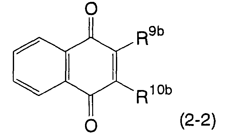
      Figure 02690001
      wherein R9b and R10b are the same or different and each denoting an alkoxy group, alkylthio group, aryloxy group or arylthio group;
      a naphthoquinone compound represented by a formula (2-3):
      Figure 02690002
      wherein R9c denotes an alkyl group or aryl group; and R12c denotes an alkyl group, alkoxy group, aryl group or aryloxy group;
      a diindenopyrazine compound represented by a formula (2-4):
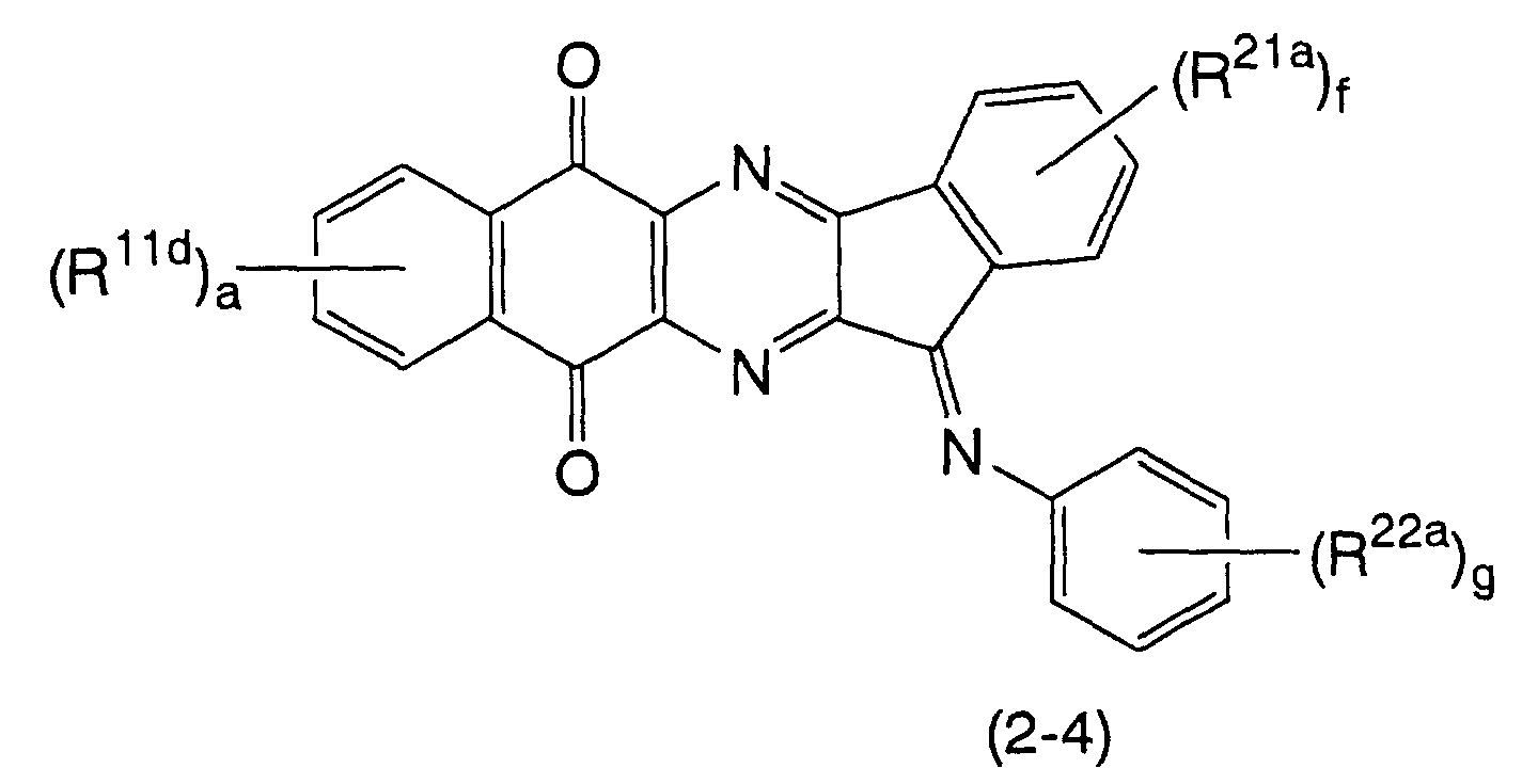
      Figure 02690003
      wherein R11d, R21a and R22a are the same or different and each denoting a hydrogen atom, halogen atom, alkyl group, alkoxy group, aryl group or aralkyl group; 'a' and 'f' are the same or different and each denoting an integer of 0 to 4; and 'g' denotes an integer of 0 to 5;
      a diindenopyrazine compound represented by a formula (2-5):
      Figure 02700001
      wherein R11e and R21b are the same or different and each denoting a hydrogen atom, halogen atom, alkyl group, alkoxy group, aryl group or aralkyl group; and 'a' and 'f' are the same or different and each denoting an integer of 0 to 4; and
      a dioxotetracenedione compound represented by a formula (2-6):
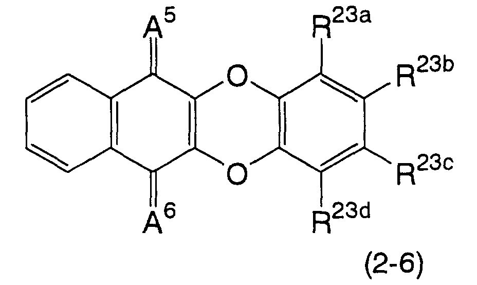
      Figure 02700002
      wherein A5 and A6 are the same or different and each denoting an oxygen atom or =N-CN group; and R23a, R23b, R23c and R23d are the same or different and each denoting a hydrogen atom, alkyl group, alkoxycarbonyl group, cycloalkyl group or group represented by a formula (2-6a):
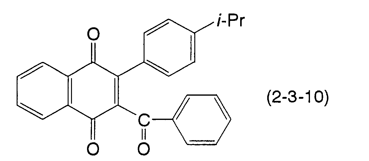
      Figure 02710001
      in which R24a, R24b, R24c, R24d and R24e are the same or different and each denoting a hydrogen atom or alkyl group.
    4. An electrophotosensitive material according to Claim 1, wherein the quinone derivative represented by the formula (4) includes at least one selected from the group consisting of a compound represented by a formula (4-1):
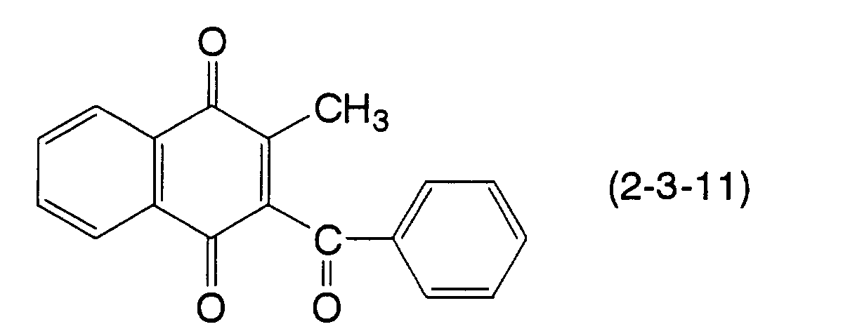
      Figure 02710002
      wherein R15a and R18a are the same or different and each denoting a hydrogen atom, halogen atom, alkyl group, alkoxy group, aryl group or aralkyl group; 'b' denotes an integer of 0 to 4, provided that when 'b' is 2 or more, the two groups R15a bonded to adjacent carbon atoms of the ring may be linked together to form a condensed ring jointly with the ring; 'c' denotes an integer of 0 to 5, provided that when 'c' is 2 or more, the groups R18a may be linked together to form a condensed ring jointly with the ring; and A1a denotes an oxygen atom or the group represented by the formula (4a);
      a compound represented by a formula (4-2):
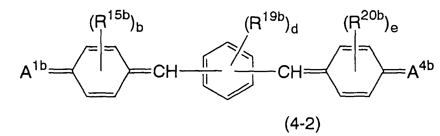
      Figure 02720001
      wherein R15b, R19b and R20b are the same or different and each denoting a hydrogen atom, halogen atom, alkyl group, alkoxy group, aryl group, cycloalkyl group, hetero cyclic group or aralkyl group; 'b', 'd' and 'e' are the same or different and each denoting an integer of 0 to 4, provided that when 'd' is 2 or more, the groups may be linked together to form a condensed ring jointly with the ring; when 'b' or 'e' is 2 or more, the corresponding two groups bonded to adjacent carbon atoms of each ring may be linked together to form a condensed ring jointly with the ring; A1b denotes an oxygen atom or the group represented by the formula (4a); and A4b denotes an oxygen atom or the group represented by the formula (4d); and a compound represented by a formula (4-3):
      Figure 02730001
      wherein R15c and R18c are the same or different and each denoting a hydrogen atom, halogen atom, alkyl group, alkoxy group, aryl group or aralkyl group; 'b' denotes an integer of 0 to 4, provided that when 'b' is 2 or more, the two groups R15c bonded to adjacent carbon atoms of the ring may be linked together to form a condensed ring jointly with the ring; 'c' denotes an integer of 0 to 5, provided that when 'c' is 2 or more, the groups R18c may be linked together to form a condensed ring jointly with the ring; and A1c denotes an oxygen atom or the group represented by the formula (4a).
    5. An electrophotosensitive material according to any preceding claim, wherein the surface protective layer is a layer formed by a vapor deposition method.
    6. An electrophotosensitive material according to any preceding claim, wherein the surface protective layer comprises at least one element selected from the group consisting of metallic elements and carbon or an inorganic compound containing any of these elements.
    7. An electrophotosensitive material according to any preceding claim, wherein the organic photosensitive layer is a single-layer photosensitive layer comprising a binder resin containing therein a charge generating material and any one of the compounds represented by the formulas (1) to (4).
    8. An electrophotosensitive material according to any one of claims 1 to 7, wherein the organic photosensitive layer is a multi-layer photosensitive layer comprising a charge generating layer and a charge transport layer laminated in this order, the charge generating layer containing a charge generating material, the charge transport layer comprising a binder resin containing therein any one of the compounds represented by the formulas (1) to (4).
    EP01307939A 2000-09-18 2001-09-18 Electrophotosensitive material Withdrawn EP1189113A3 (en)

    Applications Claiming Priority (12)

    Application Number Priority Date Filing Date Title
    JP2000281049 2000-09-18
    JP2000281049A JP2002091030A (en) 2000-09-18 2000-09-18 Electrophotographic photoreceptor
    JP2000293942A JP2002107978A (en) 2000-09-27 2000-09-27 Electrophotographic photoreceptor
    JP2000293943 2000-09-27
    JP2000293943A JP2002107979A (en) 2000-09-27 2000-09-27 Electrophotographic photoreceptor
    JP2000293942 2000-09-27
    JP2000310166A JP2002116566A (en) 2000-10-11 2000-10-11 Electrophotographic photoreceptor
    JP2000310165 2000-10-11
    JP2000310165A JP2002116565A (en) 2000-10-11 2000-10-11 Electrophotographic photoreceptor
    JP2000310166 2000-10-11
    JP2000338417A JP2002148836A (en) 2000-11-07 2000-11-07 Electrophotographic photoreceptor
    JP2000338417 2000-11-07

    Publications (2)

    Publication Number Publication Date
    EP1189113A2 true EP1189113A2 (en) 2002-03-20
    EP1189113A3 EP1189113A3 (en) 2003-10-22

    Family

    ID=27554843

    Family Applications (1)

    Application Number Title Priority Date Filing Date
    EP01307939A Withdrawn EP1189113A3 (en) 2000-09-18 2001-09-18 Electrophotosensitive material

    Country Status (2)

    Country Link
    US (1) US20020102484A1 (en)
    EP (1) EP1189113A3 (en)

    Cited By (6)

    * Cited by examiner, † Cited by third party
    Publication number Priority date Publication date Assignee Title
    CN1324027C (en) * 2003-11-21 2007-07-04 三星电子株式会社 Naphthalenetetracarboxylic acid diimide derivatives and electrophotographic photoconductive material using the derivatives
    CN102033439B (en) * 2009-09-28 2012-09-05 京瓷办公信息系统株式会社 Electrophotographic photoreceptor and method for producing the same
    CN103034077A (en) * 2011-09-30 2013-04-10 京瓷办公信息系统株式会社 Electropositive single layer type electrophotographic photoconductor and image forming device
    CN105646280A (en) * 2014-11-28 2016-06-08 京瓷办公信息系统株式会社 Quinone derivatives and electrophotographic photoreceptors
    CN105646277A (en) * 2014-11-28 2016-06-08 京瓷办公信息系统株式会社 Quinone derivatives and electrophotographic photoreceptors
    EP3191087A1 (en) * 2014-09-12 2017-07-19 Pellficure Pharmaceuticals, Inc. Compositions and methods for treatment of prostate carcinoma

    Families Citing this family (10)

    * Cited by examiner, † Cited by third party
    Publication number Priority date Publication date Assignee Title
    KR20040110662A (en) * 2003-06-20 2004-12-31 삼성전자주식회사 Naphthalenetetracarboxylic acid diimide derivatives and electrophotographic photoreceptor containing the same
    US20070077505A1 (en) * 2005-10-04 2007-04-05 Xerox Corporation Imaging member
    WO2014025370A1 (en) 2012-08-10 2014-02-13 Hallstar Innovations Corp. Tricyclic energy quencher compounds for reducing singlet oxygen generation
    US9125829B2 (en) 2012-08-17 2015-09-08 Hallstar Innovations Corp. Method of photostabilizing UV absorbers, particularly dibenzyolmethane derivatives, e.g., Avobenzone, with cyano-containing fused tricyclic compounds
    US9145383B2 (en) 2012-08-10 2015-09-29 Hallstar Innovations Corp. Compositions, apparatus, systems, and methods for resolving electronic excited states
    JP5814288B2 (en) * 2013-03-27 2015-11-17 京セラドキュメントソリューションズ株式会社 Azoquinone compound, electrophotographic photosensitive member, and image forming apparatus
    JP6520836B2 (en) * 2016-06-15 2019-05-29 京セラドキュメントソリューションズ株式会社 Quinone derivatives and electrophotographic photosensitive members
    JP6528729B2 (en) * 2016-06-15 2019-06-12 京セラドキュメントソリューションズ株式会社 Electrophotographic photoreceptor
    JP6551359B2 (en) * 2016-10-13 2019-07-31 京セラドキュメントソリューションズ株式会社 Electrophotographic photosensitive member, process cartridge, and image forming apparatus
    US10514621B2 (en) 2018-04-11 2019-12-24 Fuji Xerox Co., Ltd. Electrophotographic photoreceptor, process cartridge, image forming apparatus, and imide compound

    Family Cites Families (3)

    * Cited by examiner, † Cited by third party
    Publication number Priority date Publication date Assignee Title
    US5139906A (en) * 1989-11-30 1992-08-18 Minolta Camera Kabushiki Kaisha Photosensitive medium with a protective layer of amorphous hydrocarbon having an absorption coefficient greater than 10,000 cm-1
    US5849445A (en) * 1998-02-13 1998-12-15 Eastman Kodak Company Multilayer photoconductive elements having low dark decay
    US5882830A (en) * 1998-04-30 1999-03-16 Eastman Kodak Company Photoconductive elements having multilayer protective overcoats

    Cited By (7)

    * Cited by examiner, † Cited by third party
    Publication number Priority date Publication date Assignee Title
    CN1324027C (en) * 2003-11-21 2007-07-04 三星电子株式会社 Naphthalenetetracarboxylic acid diimide derivatives and electrophotographic photoconductive material using the derivatives
    CN102033439B (en) * 2009-09-28 2012-09-05 京瓷办公信息系统株式会社 Electrophotographic photoreceptor and method for producing the same
    CN103034077A (en) * 2011-09-30 2013-04-10 京瓷办公信息系统株式会社 Electropositive single layer type electrophotographic photoconductor and image forming device
    EP3191087A1 (en) * 2014-09-12 2017-07-19 Pellficure Pharmaceuticals, Inc. Compositions and methods for treatment of prostate carcinoma
    CN105646280A (en) * 2014-11-28 2016-06-08 京瓷办公信息系统株式会社 Quinone derivatives and electrophotographic photoreceptors
    CN105646277A (en) * 2014-11-28 2016-06-08 京瓷办公信息系统株式会社 Quinone derivatives and electrophotographic photoreceptors
    CN105646280B (en) * 2014-11-28 2018-04-17 京瓷办公信息系统株式会社 Quinone derivative and electrophotographic photoreceptor

    Also Published As

    Publication number Publication date
    EP1189113A3 (en) 2003-10-22
    US20020102484A1 (en) 2002-08-01

    Similar Documents

    Publication Publication Date Title
    EP1189113A2 (en) Electrophotosensitive material
    US6489071B2 (en) Electrophotosensitive material
    CA1337676C (en) Electrophotographic photosensitive material containing m-phenylenediamine compound
    JP2873745B2 (en) Bisstyryl compound and electrophotographic photoreceptor
    JP2002116568A (en) Electrophotographic photoreceptor
    KR930002248B1 (en) Electrophoto sensitive material
    JP3685482B2 (en) Electrophotographic photoreceptor
    JP3171755B2 (en) Electrophotographic photoreceptor
    EP1176469A1 (en) Electrosensitive material
    US6653034B2 (en) Stilbeneamine derivative and electrophotosensitive material using the same
    JP2002107978A (en) Electrophotographic photoreceptor
    JP2002116565A (en) Electrophotographic photoreceptor
    JP2002040689A (en) Electrophotographic photoreceptor
    JP2001033992A (en) Coating fluid for charge generatign layer and electrophotographic photoreceptor using same
    JP2657996B2 (en) Electrophotographic photoreceptor
    JP2002062676A (en) Electrophotographic photoreceptor
    JP2002055467A (en) Electrophotographic photoreceptor
    JP2608930B2 (en) M-phenylenediamine compound and electrophotographic photoreceptor using the same
    JP2002148834A (en) Electrophotographic photoreceptor
    JP2002148836A (en) Electrophotographic photoreceptor
    JP2002116564A (en) Electrophotographic photoreceptor
    JP2002091030A (en) Electrophotographic photoreceptor
    JP2002107979A (en) Electrophotographic photoreceptor
    JPH04330079A (en) Triphenylamine derivative and photosensitive material using the same derivative
    JP2003162082A (en) Electrophotographic photoreceptor and image forming apparatus

    Legal Events

    Date Code Title Description
    PUAI Public reference made under article 153(3) epc to a published international application that has entered the european phase

    Free format text: ORIGINAL CODE: 0009012

    AK Designated contracting states

    Kind code of ref document: A2

    Designated state(s): AT BE CH CY DE DK ES FI FR GB GR IE IT LI LU MC NL PT SE TR

    AX Request for extension of the european patent

    Free format text: AL;LT;LV;MK;RO;SI

    RIN1 Information on inventor provided before grant (corrected)

    Inventor name: FUKUNAGA, HIDEAKI, C/O KYOCERA CORPORATION

    Inventor name: INAGAKI, YOSHIO, C/O KYOCERA MITA CORPORATION

    Inventor name: MIYAMOTO, EIICHI, C/O KYOCERA MITA CORPORATION

    PUAL Search report despatched

    Free format text: ORIGINAL CODE: 0009013

    AK Designated contracting states

    Kind code of ref document: A3

    Designated state(s): AT BE CH CY DE DK ES FI FR GB GR IE IT LI LU MC NL PT SE TR

    AX Request for extension of the european patent

    Extension state: AL LT LV MK RO SI

    RIC1 Information provided on ipc code assigned before grant

    Ipc: 7G 03G 5/147 B

    Ipc: 7G 03G 5/05 B

    Ipc: 7G 03G 5/06 A

    AKX Designation fees paid
    REG Reference to a national code

    Ref country code: DE

    Ref legal event code: 8566

    STAA Information on the status of an ep patent application or granted ep patent

    Free format text: STATUS: THE APPLICATION IS DEEMED TO BE WITHDRAWN

    18D Application deemed to be withdrawn

    Effective date: 20040423